EP1903597A1 - Flächenlichtquelle, Ansteuerverfahren dafür und Hintergrundbeleuchtungseinheit mit einer solchen Lampe - Google Patents
Flächenlichtquelle, Ansteuerverfahren dafür und Hintergrundbeleuchtungseinheit mit einer solchen Lampe Download PDFInfo
- Publication number
- EP1903597A1 EP1903597A1 EP07115885A EP07115885A EP1903597A1 EP 1903597 A1 EP1903597 A1 EP 1903597A1 EP 07115885 A EP07115885 A EP 07115885A EP 07115885 A EP07115885 A EP 07115885A EP 1903597 A1 EP1903597 A1 EP 1903597A1
- Authority
- EP
- European Patent Office
- Prior art keywords
- light source
- electrode
- surface light
- electrode unit
- plate type
- Prior art date
- Legal status (The legal status is an assumption and is not a legal conclusion. Google has not performed a legal analysis and makes no representation as to the accuracy of the status listed.)
- Withdrawn
Links
Images



Classifications
-
- H—ELECTRICITY
- H01—ELECTRIC ELEMENTS
- H01J—ELECTRIC DISCHARGE TUBES OR DISCHARGE LAMPS
- H01J65/00—Lamps without any electrode inside the vessel; Lamps with at least one main electrode outside the vessel
- H01J65/04—Lamps in which a gas filling is excited to luminesce by an external electromagnetic field or by external corpuscular radiation, e.g. for indicating plasma display panels
- H01J65/042—Lamps in which a gas filling is excited to luminesce by an external electromagnetic field or by external corpuscular radiation, e.g. for indicating plasma display panels by an external electromagnetic field
- H01J65/046—Lamps in which a gas filling is excited to luminesce by an external electromagnetic field or by external corpuscular radiation, e.g. for indicating plasma display panels by an external electromagnetic field the field being produced by using capacitive means around the vessel
-
- G—PHYSICS
- G02—OPTICS
- G02F—OPTICAL DEVICES OR ARRANGEMENTS FOR THE CONTROL OF LIGHT BY MODIFICATION OF THE OPTICAL PROPERTIES OF THE MEDIA OF THE ELEMENTS INVOLVED THEREIN; NON-LINEAR OPTICS; FREQUENCY-CHANGING OF LIGHT; OPTICAL LOGIC ELEMENTS; OPTICAL ANALOGUE/DIGITAL CONVERTERS
- G02F1/00—Devices or arrangements for the control of the intensity, colour, phase, polarisation or direction of light arriving from an independent light source, e.g. switching, gating or modulating; Non-linear optics
- G02F1/01—Devices or arrangements for the control of the intensity, colour, phase, polarisation or direction of light arriving from an independent light source, e.g. switching, gating or modulating; Non-linear optics for the control of the intensity, phase, polarisation or colour
- G02F1/13—Devices or arrangements for the control of the intensity, colour, phase, polarisation or direction of light arriving from an independent light source, e.g. switching, gating or modulating; Non-linear optics for the control of the intensity, phase, polarisation or colour based on liquid crystals, e.g. single liquid crystal display cells
- G02F1/133—Constructional arrangements; Operation of liquid crystal cells; Circuit arrangements
- G02F1/1333—Constructional arrangements; Manufacturing methods
- G02F1/1335—Structural association of cells with optical devices, e.g. polarisers or reflectors
-
- H—ELECTRICITY
- H01—ELECTRIC ELEMENTS
- H01J—ELECTRIC DISCHARGE TUBES OR DISCHARGE LAMPS
- H01J61/00—Gas-discharge or vapour-discharge lamps
- H01J61/02—Details
- H01J61/04—Electrodes; Screens; Shields
- H01J61/06—Main electrodes
- H01J61/067—Main electrodes for low-pressure discharge lamps
- H01J61/0672—Main electrodes for low-pressure discharge lamps characterised by the construction of the electrode
-
- H—ELECTRICITY
- H01—ELECTRIC ELEMENTS
- H01J—ELECTRIC DISCHARGE TUBES OR DISCHARGE LAMPS
- H01J61/00—Gas-discharge or vapour-discharge lamps
- H01J61/02—Details
- H01J61/30—Vessels; Containers
- H01J61/305—Flat vessels or containers
Definitions
- the present invention relates to a surface light source, a method of driving the same, and a backlight unit having the same, and more particularly, to a surface light source capable of partially controlling brightness.
- a liquid crystal display displays an image, using the electrical and optical properties of liquid crystal.
- the liquid crystal display is widely employed in portable computers, communication devices, liquid crystal television receivers, aerospace industry, and the like because volume and weight are smaller and lighter than those of a cathode ray tube (CRT).
- CRT cathode ray tube
- the liquid crystal display includes a controlling unit to control a liquid crystal panel and a backlight source to illuminate the liquid crystal panel.
- the controlling unit includes pixel electrodes arranged on a first substrate, a common electrode disposed on a second substrate, and the liquid crystal panel disposed between the pixel electrodes and the common electrode.
- the number of the pixel electrodes is plural to achieve a resolution of the liquid crystal display, and the common electrode is single and faces the pixel electrodes.
- Thin film transistors (TFT) are connected to the pixel electrode to apply voltages of different levels thereto and a reference voltage of the same level is applied to the common electrode.
- the pixel electrodes and the common electrode are made of a transparent conductive material.
- the light illuminated by the backlight source passes through the pixel electrodes, the liquid crystal panel, and the common electrode sequentially.
- the quality of an image transmitted through the liquid crystal panel significantly depends on brightness of and brightness uniformity of the backlight source. Generally, as the brightness and the uniformity of brightness are high, the image quality becomes high.
- the backlight source of a conventional liquid crystal display chiefly employs a bar-shaped cold cathode fluorescent lamp (CCFL) or a dot-shaped light emitting diode (LED).
- the cold cathode fluorescent lamp has high brightness and long lifespan and generates heat less than that of an incandescent lamp.
- the LED has high power consumption, but has excellent brightness.
- the CCFL and the LED are disadvantageous of inferior uniformity of the brightness.
- the backlight source employing the CCFL or LED as a light source requires optical members, such as a light guide panel (LGP), a diffusion member, and a prism sheet. Due to the optical members, the liquid crystal display employing the aforementioned CCFL or LED significantly increases in size and in weigh.
- a flat fluorescent lamp (FFL) has been proposed as the backlight source of the liquid crystal display.
- a conventional surface light source 100 includes a light source body 110 and electrodes 160 provided at the outer surface of both lateral edges of the light source body 110.
- the light source body 110 includes first and second substrates facing each other by a predetermined distance.
- a plurality of partitions 140 are disposed between the first and second substrates to partition a space defined by the first and second substrates into plural discharging channels 120.
- a sealing member (not shown) is disposed at the rims of the first and second substrates to isolate the discharging channels 120 from exterior.
- a discharge gas is injected into discharging spaces 150 in the discharging channels.
- an electrode is coated on the first and second substrates or one of the first and second substrates to have the same area per a discharging channel in the form of a minus-shaped band or an island electrode.
- all the channels discharge uniformly when the surface light source is driven by an inverter.
- the surface light source maintains a predetermined degree of brightness during the driving.
- dimming technology has been proposed to vary brightness of a surface light source depending on screen information of a liquid crystal display, partially controlled brightness in a surface light source is not provided yet.
- the present invention is directed to provide a new surface light source suitable for a large-sized liquid crystal display.
- Another object of the present invention is to provide a surface light source and a backlight unit capable of partially controlling brightness.
- the present invention provides a surface light source comprising a plate type light source body having a sealed discharging space formed therein, a plate type electrode unit entirely formed on at least one surface of the light source body, and a multiple voltage applying unit to partition the electrode unit into a plurality of regions and to apply voltages to the respective regions.
- the electrode unit may comprise electrode patterns spaced apart from each other.
- each electrode unit may comprise electrode patterns formed in different directions.
- the present invention provides a driving method of a surface light source comprising forming a plate type electrode unit having a property of transmitting visible rays therethrough on a plate type light source body having a sealed discharging space, and partitioning the electrode unit into a plurality of regions and applying voltages to the respective regions.
- the present invention provides a backlight unit comprising a surface light source, a case and an inverter.
- the surface light source comprises a plate type light source body having a sealed discharging space formed therein, a plate type electrode unit entirely formed on at least one surface of the light source body, and a multiple voltage applying unit to partition the electrode unit into a plurality of regions and to apply voltages to the respective regions.
- the case accommodates the surface light source and the inverter applies voltages to first and second surface electrodes.
- the electrode unit is partitioned into plural regions and voltages are applied to respective regions so that brightness can be partially controlled. Due to this partially controlling brightness, a local dimming of the surface light source depending on screen information of a liquid crystal display is enabled, and clearer and natural image can be guaranteed.
- FIG. 2 is a perspective view illustrating a surface light source 200 according to an embodiment of the present invention
- FIG. 3 is a side view of the surface light source 200.
- the surface light source 200 includes a plate type first substrate 210 and a same type second substrate 220.
- the first substrate 210 and the second substrate 220 are preferably made of transparent thin glass substrate, and have no restriction for thickness, but may have a thickness of about 1 mm to 2 mm, preferably, less than 1 mm.
- a fluorescent layer is coated on the inner sides of the first and second substrates 210 and 220, and a reflective layer may be further formed on any one of the first and second substrates 210 and 220.
- the first substrate 210 and the second substrate 220 face each other by a predetermined distance and a sealing member 230 such as frit is inserted between edges of the substrates 210 and 220 to form a sealed space. Otherwise, the first substrate 210 and the second substrate 220 may be directly welded to each other by a heating device such as laser to form the light source body.
- the surface light source of the present invention can be implemented by a thin structure with very thin thickness.
- the light source body formed by the first substrate, the second substrate, and the sealing member includes a single open-structured inner discharging space. Moreover, since mercury-excluded gas as a discharge gas injected into the discharging space can be used, the light source body can be applied to an environmentally friendly product.
- the surface light source according to the embodiment of the present invention includes large-sized plate type electrodes formed on the outer surfaces of the light source body formed by the first and second substrates 210 and 220.
- FIG. 4 is a sectional view taken along the line X-X' in FIG. 2, and
- FIG. 5 is an enlarged view of a portion A in FIG. 4.
- a first surface electrode 250 and a second surface electrode 260 are formed on the outer surfaces of the first and second substrates 210 and 220, respectively.
- the first and second surface electrodes 250 and 260 are plate type surface electrodes to substantially cover overall area of the substrates.
- At least one of the first and second surface electrodes 250 and 260 has preferably an open ratio of 60 % or higher, of exposing a substrate such that a light transmission of light beam emitted from the light source body due to the discharging is increased.
- the first substrate 210 and the second substrate 220 are plate type substrates and the inner space defined by the first and second substrates 210 and 220 and the sealing member 230 is not an individual discharging space partitioned by the partition as the conventional surface light source, but is a single open-structured discharging space 240.
- the distance between the first and second substrates 210 and 220 is very short in comparison to the area of the substrates 210 and 220 and the inner space is the open-structure so that vacuum ventilation and the injection of the discharging gas are very easily performed.
- gas other than mercury as the discharging gas such as xenon, argon, neon, and other inactive gas, or gas mixture thereof can be used to form the surface light source.
- a vertical height of the discharging space 240 defined between the first and second substrates 210 and 220 can be determined by a spacer 235.
- the number of the spacers 235 and the interval between the spacers 235 may be determined within a range where the brightness property of light beam emitted from the surface light source is not deteriorated. Otherwise, a characteristic of the spacer may be artificially added, by molding certain parts of an upper substrate. Otherwise, the height of the discharge space 240 may be defined by protrusions (not shown) formed integrally with the inner surface of the first substrate 210 or second substrate 220. Since the discharging space is not partitioned by a partition in the surface light source according to the embodiment of the present invention, brightness and brightness uniformity of the light beam emitted from the front side of the substrates 210 and 220 are excellent.
- the first surface electrode 250 and the second surface electrode 260 may employ transparent electrodes such as ITO or electrodes with predetermined patterns.
- FIG. 6 is a sectional view illustrating a multi-layer electrode unit according to the embodiment of the present invention. As illustrated, the electrode unit has a multi-layer structure including a lower base layer 252, an electrode pattern 256 formed on the base layer 252, and a protective layer 254 formed on the base layer 252 and the electrode pattern 256.
- the base layer 252 and the protective layer 254 preferably have transparency with respect to visible rays.
- the electrode unit In a case of an electrode unit including only the electrode pattern, the electrode unit is difficult to be bonded to a glass substrate and has inferior durability. However, the multi-layer structured electrode unit is easily bonded to the glass substrate, the electrode pattern has a sufficient durability, and various electrode patterns can be formed.
- the base layer 252 is made of a material capable of resisting thermal shock such as transparent polymer, and the electrodes may be made of copper, silver, gold, aluminum, nickel, chrome, carbon or polymer based material with excellent conductivity, and mixture thereof.
- the protective layer 254 is made of transparent polymer material capable of resisting thermal shock.
- Various electrode patterns may be used in the plate type electrode unit employed in the surface light source according to the embodiment of the present invention.
- a net type electrode pattern as illustrated in FIG. 7 or a stripe type pattern as illustrated in FIGS. 8 and 9 may be used.
- circular, oval, or polygonal regular patterns may be used.
- the first surface electrode 250 formed on the first substrate 210 and the second surface electrode 260 formed on the second substrate 220 may have different electrode patterns in shape, thereby changing the discharge characteristic of the surface light source.
- the electrode patterns may be formed such that a pitch between the patterns maintains tens micro-meters to hundreds micro-meters.
- the electrode patterns may be grouped to individually apply voltages to respective groups.
- the electrode unit is partitioned into a plurality of regions and voltages are applied to the respective regions so that the brightness can be partially controlled.
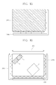
- FIGS. 10 and 11 schematically illustrate multiple divisional driving of the electrode unit of the surface light source according to the embodiment of the present invention.
- the electrode pattern of the first surface electrode (or the upper electrode) 250 is partitioned into predetermined regions and voltages are individually applied to the respective regions.
- a multiple voltage applying unit 270a can apply different voltages to the respective regions of the electrode pattern.
- the electrode pattern of the second surface electrode (or the lower electrode) 260 is partitioned into predetermined regions and voltages are individually applied to the respective regions.
- FIG. 10 illustrates an example of partitioning the electrode unit with respect to the long side of the surface light source in the vertical direction to drive the electrode unit
- FIG. 11 illustrates an example of partitioning the electrode unit with respect to the long side of the surface light source in the horizontal direction to drive the electrode unit.
- FIG. 13 illustrates that multiple voltage applying units 270a and 270b partially drive the respective regions by partitioning the electrode units when the electrode units are formed on the upper side and the lower side of the surface light source 200 so that a light emitting surface of the surface light source is controlled to have partially different brightness.
- Voltages are differently applied to the respective regions of the horizontally and vertically partitioned electrode units so that partial regions a, b, and c of the light emitting surface of the surface light source can have various brightnesss.
- the regional voltages transmitted to the multiple voltage applying units 270a and 270b are preferably controlled in association with a panel driving signal of the liquid crystal display.
- the surface light source or the backlight unit may further include an electrode data controller 275 to differently control the voltages to be applied by the multiple voltage applying units to the regions of the electrode units such that the voltages are applied to the respective regions of the electrode units in accordance with the control signal in association with a screen information of the liquid crystal display.
- FIGS. 14 and 15 illustrate electrode patterns obliquely formed different from the electrode patterns of the previous embodiment of the present invention.
- the electrode units are partitioned into a plurality of regions and multiple voltage applying units 280a and 280b drive the respective regions.
- the light emitting surface of the surface light source as illustrated in FIG. 16, may be configured such that partial regions d, e, and f have various brightnesss. If the brightness of the surface light source is partially controlled by an electrode data controller 285 in association with display information, more clear and natural high quality image can be provided.
- FIG. 17 is an exploded perspective view illustrating a backlight unit including a very thin surface light source according to an embodiment of the present invention.
- the backlight unit includes a surface light source 200, upper and lower cases 1100 and 1200, an optical sheet 900, and an inverter 1300.
- the lower case 1200 includes a bottom 1210 to accommodate the surface light source 200 and a plurality of sidewalls 1220 extended from edges of the bottom 1210 to form an accommodating space.
- the surface light source 200 is accommodated in the accommodating space of the lower case 1200.
- the inverter 1300 is disposed on the rear side of the lower case 1200 and generates a discharging voltage to drive the surface light source 200.
- the discharging voltage generated by the inverter 1300 is applied to the electrode units of the surface light source 200 through first and second power source lines 1352 and 1354.
- the optical sheet 900 may include a diffusion plate to uniformly diffuse a light beam emitted from the surface light source 200 and a prism sheet to collimate the diffused light beam.
- the upper case 1100 is coupled with the lower case 1200 to support the surface light source 200 and the optical sheet 900. The upper case 1100 prevents the surface light source 200 from being separated from the lower case 1200.
- the upper case 1100 and the lower case 1200 may be integrally formed into a single case.
- the backlight unit according to the embodiment of the present invention may not include the optical sheet 900 because of excellent brightness and brightness uniformity of the surface light source.
- the plate type electrode unit formed on the surface of the light source body of the surface light source is partitioned into a plurality of regions and voltages are applied to the respective regions so that brightness property of partially controlling brightness can be obtained.
- a locally controlled dimming of a surface light source depending on screen information of the liquid crystal display is enabled so that a high quality image can be provided.
Landscapes
- Physics & Mathematics (AREA)
- Electromagnetism (AREA)
- Plasma & Fusion (AREA)
- Engineering & Computer Science (AREA)
- Nonlinear Science (AREA)
- Crystallography & Structural Chemistry (AREA)
- Optics & Photonics (AREA)
- General Physics & Mathematics (AREA)
- Chemical & Material Sciences (AREA)
- Mathematical Physics (AREA)
- Planar Illumination Modules (AREA)
- Liquid Crystal (AREA)
- Vessels And Coating Films For Discharge Lamps (AREA)
Applications Claiming Priority (1)
| Application Number | Priority Date | Filing Date | Title |
|---|---|---|---|
| KR1020060090672A KR20080025904A (ko) | 2006-09-19 | 2006-09-19 | 면광원 장치, 그 구동 방법 및 이를 구비하는 백라이트유닛 |
Publications (1)
| Publication Number | Publication Date |
|---|---|
| EP1903597A1 true EP1903597A1 (de) | 2008-03-26 |
Family
ID=38629839
Family Applications (1)
| Application Number | Title | Priority Date | Filing Date |
|---|---|---|---|
| EP07115885A Withdrawn EP1903597A1 (de) | 2006-09-19 | 2007-09-07 | Flächenlichtquelle, Ansteuerverfahren dafür und Hintergrundbeleuchtungseinheit mit einer solchen Lampe |
Country Status (6)
| Country | Link |
|---|---|
| US (1) | US8179031B2 (de) |
| EP (1) | EP1903597A1 (de) |
| JP (1) | JP2008078135A (de) |
| KR (1) | KR20080025904A (de) |
| CN (1) | CN101149527A (de) |
| TW (1) | TW200820305A (de) |
Cited By (1)
| Publication number | Priority date | Publication date | Assignee | Title |
|---|---|---|---|---|
| US9343018B2 (en) | 2009-04-08 | 2016-05-17 | Semiconductor Energy Laboratory Co., Ltd. | Method for driving a liquid crystal display device at higher resolution |
Families Citing this family (1)
| Publication number | Priority date | Publication date | Assignee | Title |
|---|---|---|---|---|
| KR20100000195A (ko) * | 2008-06-24 | 2010-01-06 | 삼성에스디아이 주식회사 | 발광 장치 및 이 발광 장치를 광원으로 사용하는 표시 장치 |
Citations (4)
| Publication number | Priority date | Publication date | Assignee | Title |
|---|---|---|---|---|
| WO1993013514A1 (en) * | 1991-12-23 | 1993-07-08 | Panocorp Display Systems | Color fluorescent backlight for liquid crystal display |
| US6111560A (en) * | 1995-04-18 | 2000-08-29 | Cambridge Display Technology Limited | Display with a light modulator and a light source |
| US20050077808A1 (en) * | 2003-10-09 | 2005-04-14 | Patent-Treuhand-Gesellschaft Fur Elektrische Gluhlampen Mbh | Discharge lamp having at least one external electrode, and process for its production |
| JP2005107210A (ja) * | 2003-09-30 | 2005-04-21 | Fujitsu Ltd | バックライト及び液晶表示装置 |
Family Cites Families (8)
| Publication number | Priority date | Publication date | Assignee | Title |
|---|---|---|---|---|
| JP2971761B2 (ja) * | 1994-11-21 | 1999-11-08 | スタンレー電気株式会社 | 平面型蛍光ランプ |
| EP0926705A1 (de) * | 1997-12-23 | 1999-06-30 | Patent-Treuhand-Gesellschaft für elektrische Glühlampen mbH | Flachstrahler mit örtlich modulierter Flächenleuchtdichte |
| US6762556B2 (en) * | 2001-02-27 | 2004-07-13 | Winsor Corporation | Open chamber photoluminescent lamp |
| JP4032696B2 (ja) * | 2001-10-23 | 2008-01-16 | 日本電気株式会社 | 液晶表示装置 |
| US7157846B2 (en) * | 2003-06-10 | 2007-01-02 | Au Optronics Corporation | Blink plasma backlight system for liquid crystal display |
| TWI269916B (en) * | 2004-07-14 | 2007-01-01 | Delta Optoelectronics Inc | Cold cathode flat lamp and patterned electrode thereof |
| JP2006147251A (ja) * | 2004-11-17 | 2006-06-08 | Noritake Co Ltd | 平面型放電ランプ |
| KR100648782B1 (ko) * | 2004-12-23 | 2006-11-23 | 삼성코닝 주식회사 | 방전가스, 면광원 장치 및 이를 포함하는 백라이트 유닛 |
-
2006
- 2006-09-19 KR KR1020060090672A patent/KR20080025904A/ko not_active Ceased
-
2007
- 2007-09-06 TW TW096133289A patent/TW200820305A/zh unknown
- 2007-09-07 EP EP07115885A patent/EP1903597A1/de not_active Withdrawn
- 2007-09-13 JP JP2007238207A patent/JP2008078135A/ja active Pending
- 2007-09-18 US US11/901,699 patent/US8179031B2/en not_active Expired - Fee Related
- 2007-09-19 CN CNA2007101541438A patent/CN101149527A/zh active Pending
Patent Citations (4)
| Publication number | Priority date | Publication date | Assignee | Title |
|---|---|---|---|---|
| WO1993013514A1 (en) * | 1991-12-23 | 1993-07-08 | Panocorp Display Systems | Color fluorescent backlight for liquid crystal display |
| US6111560A (en) * | 1995-04-18 | 2000-08-29 | Cambridge Display Technology Limited | Display with a light modulator and a light source |
| JP2005107210A (ja) * | 2003-09-30 | 2005-04-21 | Fujitsu Ltd | バックライト及び液晶表示装置 |
| US20050077808A1 (en) * | 2003-10-09 | 2005-04-14 | Patent-Treuhand-Gesellschaft Fur Elektrische Gluhlampen Mbh | Discharge lamp having at least one external electrode, and process for its production |
Cited By (7)
| Publication number | Priority date | Publication date | Assignee | Title |
|---|---|---|---|---|
| US9343018B2 (en) | 2009-04-08 | 2016-05-17 | Semiconductor Energy Laboratory Co., Ltd. | Method for driving a liquid crystal display device at higher resolution |
| US9978320B2 (en) | 2009-04-08 | 2018-05-22 | Semiconductor Energy Laboratory Co., Ltd. | Method for driving semiconductor device |
| US10657910B2 (en) | 2009-04-08 | 2020-05-19 | Semiconductor Energy Laboratory Co., Ltd. | Method for driving semiconductor device |
| US11030966B2 (en) | 2009-04-08 | 2021-06-08 | Semiconductor Energy Laboratory Co., Ltd. | Method for driving semiconductor device |
| US11450291B2 (en) | 2009-04-08 | 2022-09-20 | Semiconductor Energy Laboratory Co., Ltd. | Method for driving semiconductor device |
| US11670251B2 (en) | 2009-04-08 | 2023-06-06 | Semiconductor Energy Laboratory Co., Ltd. | Method for driving semiconductor device |
| US12080254B2 (en) | 2009-04-08 | 2024-09-03 | Semiconductor Energy Laboratory Co., Ltd. | Method for driving semiconductor device |
Also Published As
| Publication number | Publication date |
|---|---|
| CN101149527A (zh) | 2008-03-26 |
| KR20080025904A (ko) | 2008-03-24 |
| US20080068846A1 (en) | 2008-03-20 |
| TW200820305A (en) | 2008-05-01 |
| US8179031B2 (en) | 2012-05-15 |
| JP2008078135A (ja) | 2008-04-03 |
Similar Documents
| Publication | Publication Date | Title |
|---|---|---|
| US8179031B2 (en) | Surface light source, method of driving the same, and backlight unit having the same | |
| US7764336B2 (en) | Liquid crystal display module with scattering material coating on upper surface portion of lamp | |
| US7659950B2 (en) | Liquid crystal display module having electrode pairs in partitioned light emitting spaces, respectively | |
| KR101341778B1 (ko) | 백 라이트 유닛과 이를 이용한 액정 표시장치 | |
| US20080143263A1 (en) | Surface light source device and backlight unit having the same | |
| JP2005142158A (ja) | 面光源装置及びこれを有する液晶表示装置 | |
| KR20080008194A (ko) | 평판 전극, 이를 포함하는 초박형 면광원 장치 및 백라이트유닛 | |
| KR20080068947A (ko) | 셀전극을 구비하는 면광원 장치 및 이를 포함하는 백라이트유닛 | |
| KR100971395B1 (ko) | 백 라이트 유닛 | |
| KR20080020116A (ko) | 이차전자방출층이 형성된 면광원 장치, 그 제조 방법 및이를 구비하는 백라이트 유닛 | |
| KR20080023003A (ko) | 면광원 장치 및 이를 구비하는 백라이트 유닛 | |
| KR20070118506A (ko) | 반사막 겸용 평판형 전극을 포함하는 면광원 장치 및 이를구비하는 백라이트 유닛 | |
| KR20080045980A (ko) | 불균일 형광층을 포함하는 면광원 장치용 기판, 이를포함하는 면광원 장치 및 백라이트 유닛 | |
| KR20070118505A (ko) | 스페이서 일체형 기판을 포함하는 면광원 장치 및 이를구비하는 백라이트 유닛 | |
| KR20070118504A (ko) | 확산층을 포함하는 복합 전극, 부착형 확산층을 포함하는면광원 장치 및 이를 구비하는 백라이트 유닛 | |
| KR20080032884A (ko) | 면광원 장치 및 이를 구비하는 백라이트 유닛 | |
| KR20070119909A (ko) | 이중 전극 패턴을 포함하는 초박형 면광원 장치 및 이를구비하는 백라이트 유닛 | |
| KR20080072236A (ko) | 초박형 면광원 장치 및 이를 구비하는 백라이트 유닛 | |
| KR20080065771A (ko) | 방전셀 매트릭스를 구비하는 면광원 장치 및 이를 포함하는백라이트 유닛 | |
| KR20090012674A (ko) | 면광원 장치 및 이를 포함하는 백라이트 유닛 | |
| KR20080032527A (ko) | 면광원 장치의 스페이서 형성 장치, 면광원 장치 및 이를구비하는 백라이트 유닛 | |
| KR20080107607A (ko) | 대면적 면광원 장치 및 백라이트 유닛 | |
| KR20080013177A (ko) | 초박형 면광원 장치 및 이를 구비하는 백라이트 유닛 | |
| KR20080053770A (ko) | 면광원 장치 및 이를 구비하는 백라이트 유닛 | |
| KR20090012675A (ko) | 면광원 장치, 그 제조 방법 및 이를 포함하는 백라이트유닛 |
Legal Events
| Date | Code | Title | Description |
|---|---|---|---|
| PUAI | Public reference made under article 153(3) epc to a published international application that has entered the european phase |
Free format text: ORIGINAL CODE: 0009012 |
|
| AK | Designated contracting states |
Kind code of ref document: A1 Designated state(s): AT BE BG CH CY CZ DE DK EE ES FI FR GB GR HU IE IS IT LI LT LU LV MC MT NL PL PT RO SE SI SK TR |
|
| AX | Request for extension of the european patent |
Extension state: AL BA HR MK YU |
|
| RAP1 | Party data changed (applicant data changed or rights of an application transferred) |
Owner name: SAMSUNG CORNING PRECISION GLASS CO., LTD. |
|
| RIN1 | Information on inventor provided before grant (corrected) |
Inventor name: JEE, YONG KEUN Inventor name: KEE, WON DO Inventor name: LEE, DONG HEE Inventor name: LEE, KEUN SEOK Inventor name: YOUN, HYUNG BIN Inventor name: JUNG, KYEONG TAEK Inventor name: LEE, KI YEON Inventor name: BAN, SEOK MO |
|
| AKX | Designation fees paid |
Designated state(s): DE FR GB |
|
| STAA | Information on the status of an ep patent application or granted ep patent |
Free format text: STATUS: THE APPLICATION IS DEEMED TO BE WITHDRAWN |
|
| 18D | Application deemed to be withdrawn |
Effective date: 20080927 |