EP1903615A1 - Verfahren zur Metallisierung mehrfach wärmebehandelter photovoltaischer Solarzellen - Google Patents
Verfahren zur Metallisierung mehrfach wärmebehandelter photovoltaischer Solarzellen Download PDFInfo
- Publication number
- EP1903615A1 EP1903615A1 EP07116751A EP07116751A EP1903615A1 EP 1903615 A1 EP1903615 A1 EP 1903615A1 EP 07116751 A EP07116751 A EP 07116751A EP 07116751 A EP07116751 A EP 07116751A EP 1903615 A1 EP1903615 A1 EP 1903615A1
- Authority
- EP
- European Patent Office
- Prior art keywords
- substrate
- photovoltaic cell
- metallization
- layer
- front face
- Prior art date
- Legal status (The legal status is an assumption and is not a legal conclusion. Google has not performed a legal analysis and makes no representation as to the accuracy of the status listed.)
- Granted
Links
- 238000000034 method Methods 0.000 title claims abstract description 41
- 238000001465 metallisation Methods 0.000 title claims abstract description 40
- 239000000758 substrate Substances 0.000 claims abstract description 75
- 229910052739 hydrogen Inorganic materials 0.000 claims abstract description 17
- 239000001257 hydrogen Substances 0.000 claims abstract description 17
- UFHFLCQGNIYNRP-UHFFFAOYSA-N Hydrogen Chemical compound [H][H] UFHFLCQGNIYNRP-UHFFFAOYSA-N 0.000 claims abstract description 13
- 229910052782 aluminium Inorganic materials 0.000 claims abstract description 6
- XAGFODPZIPBFFR-UHFFFAOYSA-N aluminium Chemical compound [Al] XAGFODPZIPBFFR-UHFFFAOYSA-N 0.000 claims abstract description 6
- 229910052709 silver Inorganic materials 0.000 claims abstract description 6
- 239000004332 silver Substances 0.000 claims abstract description 6
- 229910052581 Si3N4 Inorganic materials 0.000 claims abstract description 5
- HQVNEWCFYHHQES-UHFFFAOYSA-N silicon nitride Chemical compound N12[Si]34N5[Si]62N3[Si]51N64 HQVNEWCFYHHQES-UHFFFAOYSA-N 0.000 claims abstract description 5
- 229910021420 polycrystalline silicon Inorganic materials 0.000 claims abstract description 4
- 238000000137 annealing Methods 0.000 claims description 29
- 238000009792 diffusion process Methods 0.000 claims description 7
- 238000005984 hydrogenation reaction Methods 0.000 claims description 7
- KWYUFKZDYYNOTN-UHFFFAOYSA-M Potassium hydroxide Chemical compound [OH-].[K+] KWYUFKZDYYNOTN-UHFFFAOYSA-M 0.000 claims description 5
- 229910052698 phosphorus Inorganic materials 0.000 claims description 5
- 238000000151 deposition Methods 0.000 claims description 4
- 238000000623 plasma-assisted chemical vapour deposition Methods 0.000 claims description 4
- 238000007650 screen-printing Methods 0.000 claims description 4
- 239000004065 semiconductor Substances 0.000 claims description 4
- OAICVXFJPJFONN-UHFFFAOYSA-N Phosphorus Chemical compound [P] OAICVXFJPJFONN-UHFFFAOYSA-N 0.000 claims description 3
- 239000011574 phosphorus Substances 0.000 claims description 3
- BQCADISMDOOEFD-UHFFFAOYSA-N Silver Chemical compound [Ag] BQCADISMDOOEFD-UHFFFAOYSA-N 0.000 abstract description 2
- 239000011247 coating layer Substances 0.000 abstract 1
- 230000007547 defect Effects 0.000 description 10
- 239000012535 impurity Substances 0.000 description 9
- 238000002161 passivation Methods 0.000 description 9
- XUIMIQQOPSSXEZ-UHFFFAOYSA-N Silicon Chemical compound [Si] XUIMIQQOPSSXEZ-UHFFFAOYSA-N 0.000 description 8
- 229910052710 silicon Inorganic materials 0.000 description 8
- 239000010703 silicon Substances 0.000 description 8
- 238000004519 manufacturing process Methods 0.000 description 6
- 239000000463 material Substances 0.000 description 6
- 230000015572 biosynthetic process Effects 0.000 description 5
- 239000000969 carrier Substances 0.000 description 5
- 229910045601 alloy Inorganic materials 0.000 description 4
- 239000000956 alloy Substances 0.000 description 4
- -1 hydrogen ions Chemical class 0.000 description 4
- 230000000694 effects Effects 0.000 description 3
- 238000005530 etching Methods 0.000 description 3
- 229910052751 metal Inorganic materials 0.000 description 3
- 239000002184 metal Substances 0.000 description 3
- 238000000206 photolithography Methods 0.000 description 3
- KDLHZDBZIXYQEI-UHFFFAOYSA-N Palladium Chemical compound [Pd] KDLHZDBZIXYQEI-UHFFFAOYSA-N 0.000 description 2
- 239000011248 coating agent Substances 0.000 description 2
- 238000000576 coating method Methods 0.000 description 2
- 238000010494 dissociation reaction Methods 0.000 description 2
- 230000005593 dissociations Effects 0.000 description 2
- 230000005669 field effect Effects 0.000 description 2
- 150000002500 ions Chemical class 0.000 description 2
- 238000007639 printing Methods 0.000 description 2
- ZOXJGFHDIHLPTG-UHFFFAOYSA-N Boron Chemical compound [B] ZOXJGFHDIHLPTG-UHFFFAOYSA-N 0.000 description 1
- UFHFLCQGNIYNRP-VVKOMZTBSA-N Dideuterium Chemical compound [2H][2H] UFHFLCQGNIYNRP-VVKOMZTBSA-N 0.000 description 1
- RTAQQCXQSZGOHL-UHFFFAOYSA-N Titanium Chemical compound [Ti] RTAQQCXQSZGOHL-UHFFFAOYSA-N 0.000 description 1
- 238000000637 aluminium metallisation Methods 0.000 description 1
- 229910052796 boron Inorganic materials 0.000 description 1
- 238000005266 casting Methods 0.000 description 1
- 238000006243 chemical reaction Methods 0.000 description 1
- 229910021419 crystalline silicon Inorganic materials 0.000 description 1
- 230000008021 deposition Effects 0.000 description 1
- 230000008020 evaporation Effects 0.000 description 1
- 238000001704 evaporation Methods 0.000 description 1
- 230000002349 favourable effect Effects 0.000 description 1
- 239000000945 filler Substances 0.000 description 1
- 238000010438 heat treatment Methods 0.000 description 1
- 238000009776 industrial production Methods 0.000 description 1
- 238000013508 migration Methods 0.000 description 1
- 230000005012 migration Effects 0.000 description 1
- 230000003287 optical effect Effects 0.000 description 1
- 229910052763 palladium Inorganic materials 0.000 description 1
- 238000012545 processing Methods 0.000 description 1
- 238000002310 reflectometry Methods 0.000 description 1
- 238000005204 segregation Methods 0.000 description 1
- HBMJWWWQQXIZIP-UHFFFAOYSA-N silicon carbide Chemical compound [Si+]#[C-] HBMJWWWQQXIZIP-UHFFFAOYSA-N 0.000 description 1
- 229910010271 silicon carbide Inorganic materials 0.000 description 1
- 238000010561 standard procedure Methods 0.000 description 1
- 230000001629 suppression Effects 0.000 description 1
- 229910052719 titanium Inorganic materials 0.000 description 1
- 239000010936 titanium Substances 0.000 description 1
- 238000012546 transfer Methods 0.000 description 1
Images


Classifications
-
- H—ELECTRICITY
- H10—SEMICONDUCTOR DEVICES; ELECTRIC SOLID-STATE DEVICES NOT OTHERWISE PROVIDED FOR
- H10F—INORGANIC SEMICONDUCTOR DEVICES SENSITIVE TO INFRARED RADIATION, LIGHT, ELECTROMAGNETIC RADIATION OF SHORTER WAVELENGTH OR CORPUSCULAR RADIATION
- H10F71/00—Manufacture or treatment of devices covered by this subclass
- H10F71/128—Annealing
-
- H—ELECTRICITY
- H10—SEMICONDUCTOR DEVICES; ELECTRIC SOLID-STATE DEVICES NOT OTHERWISE PROVIDED FOR
- H10F—INORGANIC SEMICONDUCTOR DEVICES SENSITIVE TO INFRARED RADIATION, LIGHT, ELECTROMAGNETIC RADIATION OF SHORTER WAVELENGTH OR CORPUSCULAR RADIATION
- H10F77/00—Constructional details of devices covered by this subclass
- H10F77/20—Electrodes
- H10F77/206—Electrodes for devices having potential barriers
- H10F77/211—Electrodes for devices having potential barriers for photovoltaic cells
-
- Y—GENERAL TAGGING OF NEW TECHNOLOGICAL DEVELOPMENTS; GENERAL TAGGING OF CROSS-SECTIONAL TECHNOLOGIES SPANNING OVER SEVERAL SECTIONS OF THE IPC; TECHNICAL SUBJECTS COVERED BY FORMER USPC CROSS-REFERENCE ART COLLECTIONS [XRACs] AND DIGESTS
- Y02—TECHNOLOGIES OR APPLICATIONS FOR MITIGATION OR ADAPTATION AGAINST CLIMATE CHANGE
- Y02E—REDUCTION OF GREENHOUSE GAS [GHG] EMISSIONS, RELATED TO ENERGY GENERATION, TRANSMISSION OR DISTRIBUTION
- Y02E10/00—Energy generation through renewable energy sources
- Y02E10/50—Photovoltaic [PV] energy
- Y02E10/547—Monocrystalline silicon PV cells
-
- Y—GENERAL TAGGING OF NEW TECHNOLOGICAL DEVELOPMENTS; GENERAL TAGGING OF CROSS-SECTIONAL TECHNOLOGIES SPANNING OVER SEVERAL SECTIONS OF THE IPC; TECHNICAL SUBJECTS COVERED BY FORMER USPC CROSS-REFERENCE ART COLLECTIONS [XRACs] AND DIGESTS
- Y02—TECHNOLOGIES OR APPLICATIONS FOR MITIGATION OR ADAPTATION AGAINST CLIMATE CHANGE
- Y02P—CLIMATE CHANGE MITIGATION TECHNOLOGIES IN THE PRODUCTION OR PROCESSING OF GOODS
- Y02P70/00—Climate change mitigation technologies in the production process for final industrial or consumer products
- Y02P70/50—Manufacturing or production processes characterised by the final manufactured product
Definitions
- the invention relates to the field of photovoltaic cells and more particularly to a method of metallization of photovoltaic cells.
- FIGS. 1A to 1E A standard method used for the industrial production of a crystalline silicon (monocrystalline or multicrystalline) photovoltaic cell of the P or N type is shown in FIGS. 1A to 1E.
- An N or P type substrate 2 first undergoes texturing of its surfaces by the use of a potassium hydroxide solution, which makes it possible to reduce the reflectivity of these surfaces and thus to obtain better optical confinement of the incoming beams in the substrate 2.
- An N + type layer 4 is formed in the substrate 2 by phosphorus diffusion at all the faces of the substrate 2 (FIG. 1A).
- An anti-reflection layer 6 of hydrogen-rich silicon nitride ( SiN - H ) is then deposited on the N + 4 layer by plasma-enhanced chemical vapor deposition (PECVD), as shown in FIG. 1B, forming a front face 8 of the photovoltaic cell 20.
- PECVD plasma-enhanced chemical vapor deposition
- Silver and aluminum metallizations 12 are formed by screen printing respectively on the front face 8 and on the rear face of the substrate 2 (FIG. 1C).
- these metallizations 10, 12 are annealed in an oven an infrared passage, forming contacts 14 between the metallizations before 10 and the N + layer 4, and a layer 16 based on an alloy of aluminum and silicon, and a layer 18 of P + type in the substrate 2, replacing a portion of the N + layer 4 under the rear metallization 12.
- the part of the remaining N + 4 layer and the substrate 2 form the PN junction of the photovoltaic cell 20.
- the P + layer 18 allows passivation of the rear face of the substrate 2 by a rear-field effect (BSF) pushing minority carriers, here electrons, in the substrate 2.
- BSF rear-field effect
- the photovoltaic cell 20, and the N + layer 4 passivates the front face of the substrate 2 by a forward field effect (FSF) pushing minority carriers, here holes, in the substrate 2, the anti-reflection layer 6 also contributing to this passivation.
- FSF forward field effect
- the document "N-type multicrystalline silicon for solar cells" by S. Martinuzzi et al, 20th EPSEC, 2005, Barcelona, pages 631 to 634 describes such a photovoltaic cell, the annealing temperature described being between 850 ° C and 900 ° C.
- this alloy layer 16 makes it possible to improve the quality of the silicon of the substrate 2 by the getter effect by trapping the impurities by a segregation mechanism .
- This hydrogenation phenomenon during annealing is described in the document "Hydrogen passivation of defects in multicrystalline silicon solar cells” by S. Martinuzzi et al., Solar Energy Materials & Solar Cells, vol. 80, pp. 343-353, 2003 .
- the diffusion of hydrogen into the substrate 2 is particularly effective when extended crystallographic defect densities, such as dislocations or twin joints, are important. Passivation by hydrogen is very useful when concentrations of impurities, mainly metallic, are important, for example in materials made from poor quality fillers (metallurgical silicon charges), or dislocation-rich materials such as those resulting from electromagnetic continuous flows or prints in ribbon.
- An object of the present invention is to propose a process for metallization of photovoltaic cells making it possible to obtain photovoltaic cells having a better efficiency than the cells produced according to the methods of the art. previously described, and which is economically viable in the industry.
- the method applies to both N-type and P-type substrates.
- a substrate 102 of a first type of conductivity for example based on silicon multicrystalline or monocrystalline P type, is shown in Figure 2A.
- the surfaces of the substrate 102 are first texturized by the use of a potassium hydroxide solution.
- a doped layer 104 of a second type of conductivity for example of the N + type, is then formed by phosphorus diffusion in the substrate 102.
- This layer 104 forms, in particular, a front face of the substrate 102 on which is deposited, for example by PECVD , an antireflection layer 106, for example rich in hydrogen and based on silicon nitride or silicon carbide, and forming a front face 108 of the photovoltaic cell 100.
- the PN junction of the photovoltaic cell 100 is formed by the substrate 102 P type and N + layer 104.
- a hydrogenation step of the substrate 102 can be carried out during the process. This step may be performed for example before and / or after the deposition of the antireflection layer 106.
- metallizations 110 for example based on silver, are made for example by screen printing on the front face 108 of the photovoltaic cell 100.
- the metallizations 110 may also be based on at least one other metal as silver, and formed by other techniques such as photolithography or printing.
- the solar cell 100 is then placed for example in an infrared oven for undergo a first annealing.
- This first annealing is carried out at a temperature of between about 800 ° C. and 900 ° C., thus forming contacts 114 between the metallizations 110 and the N + layer 104 (FIG. 2B).
- hydrogen migrates in the form of ions from the hydrogen-rich antireflection layer 106 in the substrate 102, achieving passivation of the crystallographic defects and impurities of the substrate 102.
- This first annealing may also be performed in a conventional annealing furnace, or by other known annealing techniques. For example, this first annealing is carried out at a temperature of about 850 ° C for a period of between about 1 second and 10 seconds.
- a metallization layer 112 for example based on aluminum, is then produced on the rear face of the substrate 102 (see FIG. 2C).
- This metallization layer 112 may for example be made by screen printing, or by photolithography or printing.
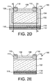
- a second annealing of the photovoltaic cell 100 is then carried out, for example in an infrared oven at a temperature of between about 700 ° C. and 800 ° C. (see FIG. 2D).
- This second annealing allows a better passivation of the defects and impurities of the substrate 102 because this temperature range is more favorable for the formation of bonds between the hydrogen and the impurities or the crystallographic defects than the temperature range of the first annealing (included between about 800 ° C and 900 ° C), allowing the dissociation of H 2 molecules formed by the migration of hydrogen ions from the antireflection layer 106 in the substrate 102 and / or implanted in the substrate 102 by a hydrogenation step of the substrate 102.
- This second annealing temperature of between about 700 ° C. and 800 ° C. constitutes an ideal compromise between the intensity of the diffusion of the hydrogen ions and their capacity to form bonds with the impurities or the defects in the substrate 102.
- This second annealing can also be carried out in a conventional annealing furnace, or by means of other known annealing techniques.
- This second annealing results in the formation of a P + doped layer 118 in the substrate 102 and the formation of a layer 116 based on an alloy of aluminum and silicon, replacing the N + layer 104 under the rear metallization 112.
- the P + doped layer 118 passivates the rear face of the substrate 102 by a rear-field effect (BSF) pushing back minority carriers in the substrate 102.
- BSF rear-field effect
- a metal other than aluminum may also be used for the realization of the metallization layer 112. This metal will be chosen so as to also obtain a P + doped layer 118.
- This second annealing can also be optimized by choosing an annealing temperature equal to about 770 ° C for a period of time between about 1 second and 10 seconds, allowing in particular to obtain a good hydrogenation of the substrate 102.
- the method according to the invention is also particularly suitable for the production of photovoltaic cells comprising N type substrates.
- the P + doped layer 118 acts as a transmitter of the PN junction of the photovoltaic cell.
- the N + doped layer 104 then performs the passivation of the front face of the substrate 102 by a forward field effect (FSF) pushing back minority carriers in the substrate 102, the antireflection layer 106 also contributing to this passivation.
- FSF forward field effect
- the doped layer of the second conductivity type 104 to be a P + doped layer, obtained for example by boron diffusion in the substrate 102.
- the photovoltaic cell it is possible for the photovoltaic cell to undergo a third annealing at a low temperature, for example between about 200 ° C. and 500 ° C.
- This third annealing which can be carried out at ambient pressure, allows the hydrogen present in the substrate 102 to form additional bonds with crystallographic defects or impurities present in the substrate 102.
Landscapes
- Photovoltaic Devices (AREA)
- Manufacture And Refinement Of Metals (AREA)
- Processing Of Solid Wastes (AREA)
Applications Claiming Priority (1)
| Application Number | Priority Date | Filing Date | Title |
|---|---|---|---|
| FR0653884A FR2906404B1 (fr) | 2006-09-21 | 2006-09-21 | Procede de metallisation de cellules photovoltaiques a multiples recuits |
Publications (2)
| Publication Number | Publication Date |
|---|---|
| EP1903615A1 true EP1903615A1 (de) | 2008-03-26 |
| EP1903615B1 EP1903615B1 (de) | 2009-11-11 |
Family
ID=38006568
Family Applications (1)
| Application Number | Title | Priority Date | Filing Date |
|---|---|---|---|
| EP07116751A Not-in-force EP1903615B1 (de) | 2006-09-21 | 2007-09-19 | Verfahren zur Metallisierung mehrfach wärmebehandelter photovoltaischer Solarzellen |
Country Status (7)
| Country | Link |
|---|---|
| US (1) | US7943417B2 (de) |
| EP (1) | EP1903615B1 (de) |
| JP (1) | JP5296357B2 (de) |
| AT (1) | ATE448570T1 (de) |
| DE (1) | DE602007003166D1 (de) |
| ES (1) | ES2336615T3 (de) |
| FR (1) | FR2906404B1 (de) |
Cited By (2)
| Publication number | Priority date | Publication date | Assignee | Title |
|---|---|---|---|---|
| JP2009267380A (ja) * | 2008-04-03 | 2009-11-12 | Commissariat A L'energie Atomique | 軽元素の熱活性化により半導体基板を処理する方法 |
| JP2014531766A (ja) * | 2011-09-29 | 2014-11-27 | インリー エナジー(チャイナ)カンパニー リミテッド | 太陽電池シート及びその熱処理プロセス |
Families Citing this family (15)
| Publication number | Priority date | Publication date | Assignee | Title |
|---|---|---|---|---|
| DE102007054384A1 (de) * | 2007-11-14 | 2009-05-20 | Institut Für Solarenergieforschung Gmbh | Verfahren zum Herstellen einer Solarzelle mit einer oberflächenpassivierenden Dielektrikumdoppelschicht und entsprechende Solarzelle |
| US8309446B2 (en) | 2008-07-16 | 2012-11-13 | Applied Materials, Inc. | Hybrid heterojunction solar cell fabrication using a doping layer mask |
| US8664524B2 (en) | 2008-07-17 | 2014-03-04 | Uriel Solar, Inc. | High power efficiency, large substrate, polycrystalline CdTe thin film semiconductor photovoltaic cell structures grown by molecular beam epitaxy at high deposition rate for use in solar electricity generation |
| WO2010068331A1 (en) | 2008-12-10 | 2010-06-17 | Applied Materials, Inc. | Enhanced vision system for screen printing pattern alignment |
| JP5183588B2 (ja) * | 2009-07-15 | 2013-04-17 | 三菱電機株式会社 | 光起電力装置の製造方法 |
| US9064999B2 (en) | 2009-09-07 | 2015-06-23 | Lg Electronics Inc. | Solar cell and method for manufacturing the same |
| CN102044579B (zh) | 2009-09-07 | 2013-12-18 | Lg电子株式会社 | 太阳能电池 |
| JP5477303B2 (ja) * | 2011-01-12 | 2014-04-23 | 信越化学工業株式会社 | 太陽電池の製造方法 |
| KR101902887B1 (ko) * | 2011-12-23 | 2018-10-01 | 엘지전자 주식회사 | 태양 전지의 제조 방법 |
| US20130199604A1 (en) * | 2012-02-06 | 2013-08-08 | Silicon Solar Solutions | Solar cells and methods of fabrication thereof |
| JP2015519729A (ja) * | 2012-04-02 | 2015-07-09 | ヌソラ インコーポレイテッドnusola Inc. | 光電変換素子及びその製造方法 |
| KR101264367B1 (ko) * | 2012-07-13 | 2013-05-14 | 한국기계연구원 | 투명 전도성 반사방지막을 갖는 광전 소자 |
| US9960287B2 (en) | 2014-02-11 | 2018-05-01 | Picasolar, Inc. | Solar cells and methods of fabrication thereof |
| KR101569415B1 (ko) * | 2014-06-09 | 2015-11-16 | 엘지전자 주식회사 | 태양 전지의 제조 방법 |
| US10593818B2 (en) * | 2016-12-09 | 2020-03-17 | The Boeing Company | Multijunction solar cell having patterned emitter and method of making the solar cell |
Citations (2)
| Publication number | Priority date | Publication date | Assignee | Title |
|---|---|---|---|---|
| US4577393A (en) * | 1983-11-11 | 1986-03-25 | Telefunken Electronic Gmbh | Process for the production of a solar cell |
| US20050189015A1 (en) * | 2003-10-30 | 2005-09-01 | Ajeet Rohatgi | Silicon solar cells and methods of fabrication |
Family Cites Families (15)
| Publication number | Priority date | Publication date | Assignee | Title |
|---|---|---|---|---|
| US4680085A (en) * | 1986-04-14 | 1987-07-14 | Ovonic Imaging Systems, Inc. | Method of forming thin film semiconductor devices |
| JPH0754854B2 (ja) * | 1987-02-20 | 1995-06-07 | 京セラ株式会社 | 太陽電池素子及びその製造方法 |
| JPH03101170A (ja) * | 1989-09-13 | 1991-04-25 | Sharp Corp | 太陽電池の製造方法 |
| US5688366A (en) * | 1994-04-28 | 1997-11-18 | Canon Kabushiki Kaisha | Etching method, method of producing a semiconductor device, and etchant therefor |
| FR2722612B1 (fr) * | 1994-07-13 | 1997-01-03 | Centre Nat Rech Scient | Procede de fabrication d'un materiau ou dispositif photovoltaique, materiau ou dispositif ainsi obteu et photopile comprenant un tel materiau ou dispositif |
| JP2006148155A (ja) * | 1994-07-21 | 2006-06-08 | Sharp Corp | 太陽電池の製造方法および太陽電池 |
| JP3722326B2 (ja) * | 1996-12-20 | 2005-11-30 | 三菱電機株式会社 | 太陽電池の製造方法 |
| JP2002289889A (ja) * | 2001-03-23 | 2002-10-04 | Mitsubishi Electric Corp | 太陽電池モジュール |
| JP2004296801A (ja) * | 2003-03-27 | 2004-10-21 | Kyocera Corp | 太陽電池素子 |
| JP2005135942A (ja) * | 2003-10-28 | 2005-05-26 | Canon Inc | 電極配設方法 |
| JP2005154795A (ja) * | 2003-11-21 | 2005-06-16 | Sharp Corp | 薄膜の製造方法および太陽電池 |
| JP4326314B2 (ja) * | 2003-12-08 | 2009-09-02 | シャープ株式会社 | 太陽電池の製造方法 |
| JP2006012913A (ja) * | 2004-06-22 | 2006-01-12 | Sharp Corp | 太陽電池セルの製造方法 |
| JP2006128391A (ja) * | 2004-10-28 | 2006-05-18 | Sharp Corp | 結晶質シリコン基板のその処理方法および光電変換素子 |
| JP4565976B2 (ja) * | 2004-11-24 | 2010-10-20 | 京セラ株式会社 | 太陽電池モジュール |
-
2006
- 2006-09-21 FR FR0653884A patent/FR2906404B1/fr not_active Expired - Fee Related
-
2007
- 2007-08-28 US US11/845,871 patent/US7943417B2/en not_active Expired - Fee Related
- 2007-09-19 ES ES07116751T patent/ES2336615T3/es active Active
- 2007-09-19 DE DE602007003166T patent/DE602007003166D1/de active Active
- 2007-09-19 EP EP07116751A patent/EP1903615B1/de not_active Not-in-force
- 2007-09-19 AT AT07116751T patent/ATE448570T1/de not_active IP Right Cessation
- 2007-09-20 JP JP2007244235A patent/JP5296357B2/ja not_active Expired - Fee Related
Patent Citations (2)
| Publication number | Priority date | Publication date | Assignee | Title |
|---|---|---|---|---|
| US4577393A (en) * | 1983-11-11 | 1986-03-25 | Telefunken Electronic Gmbh | Process for the production of a solar cell |
| US20050189015A1 (en) * | 2003-10-30 | 2005-09-01 | Ajeet Rohatgi | Silicon solar cells and methods of fabrication |
Non-Patent Citations (3)
| Title |
|---|
| NIJS J F ET AL: "Advanced Manufacturing Concepts for Crystalline Silicon Solar Cells", IEEE TRANSACTIONS ON ELECTRON DEVICES, IEEE SERVICE CENTER, PISACATAWAY, NJ, US, vol. 46, no. 10, October 1999 (1999-10-01), pages 1948 - 1969, XP011017056, ISSN: 0018-9383 * |
| OKAMOTO S ET AL: "23.5% efficient silicon solar cell with rear micro contacts of c-Si spl mu/c-Si:H heterostructure", CONFERENCE RECORD OF THE 26TH IEEE PHOTOVOLTAIC SPECIALISTS CONFERENCE, 29 September 1997 (1997-09-29), pages 255 - 258, XP010267775, ISBN: 0-7803-3767-0 * |
| SANA P ET AL: "The effect of aluminum treatment and forming gas anneal on EFG silicon solar cells", PROCEEDINGS OF THE PHOTOVOLTAIC SPECIALISTS CONFERENCE. LOUISVILLE, MAY 10 - 14, 1993, NEW YORK, IEEE, US, vol. CONF. 23, 10 May 1993 (1993-05-10), pages 111 - 116, XP010113294, ISBN: 0-7803-1220-1 * |
Cited By (2)
| Publication number | Priority date | Publication date | Assignee | Title |
|---|---|---|---|---|
| JP2009267380A (ja) * | 2008-04-03 | 2009-11-12 | Commissariat A L'energie Atomique | 軽元素の熱活性化により半導体基板を処理する方法 |
| JP2014531766A (ja) * | 2011-09-29 | 2014-11-27 | インリー エナジー(チャイナ)カンパニー リミテッド | 太陽電池シート及びその熱処理プロセス |
Also Published As
| Publication number | Publication date |
|---|---|
| DE602007003166D1 (de) | 2009-12-24 |
| ES2336615T3 (es) | 2010-04-14 |
| JP5296357B2 (ja) | 2013-09-25 |
| US20080076203A1 (en) | 2008-03-27 |
| EP1903615B1 (de) | 2009-11-11 |
| US7943417B2 (en) | 2011-05-17 |
| FR2906404A1 (fr) | 2008-03-28 |
| ATE448570T1 (de) | 2009-11-15 |
| FR2906404B1 (fr) | 2008-12-19 |
| JP2008078661A (ja) | 2008-04-03 |
Similar Documents
| Publication | Publication Date | Title |
|---|---|---|
| EP1903615B1 (de) | Verfahren zur Metallisierung mehrfach wärmebehandelter photovoltaischer Solarzellen | |
| EP1903616B1 (de) | Verfahren zum Tempern von Sperrschichtphotozellen | |
| EP1903617B1 (de) | Verfahren zur Herstellung von dotierten Bereichen in einem Substrat und von Sperrschichtphotozellen | |
| EP3900052B1 (de) | Verfahren zur passivierung von fotovoltaischen zellen und verfahren zur herstellung passivierter fotovoltaischer unterzellen | |
| EP2172981B1 (de) | Fotovoltaikzelle mit Heteroübergang mit zwei Dotierungen und Herstellungsverfahren | |
| EP2067174A2 (de) | Verfahren zum herstellen einer fotovoltaischen zelle mit einem heteroübergang auf der rückseite | |
| EP2091086A2 (de) | Halbleitervorrichtung mit Heteroübergängen | |
| FR2929755A1 (fr) | Procede de traitement d'un substrat semi-conducteur par activation thermique d'elements legers | |
| CN102893404A (zh) | 用于局部高掺杂和接通是太阳能电池或太阳能电池前体的半导体结构的方法 | |
| EP3331031B1 (de) | Verfahren zur herstellung einer fotovoltaikzelle und fotovoltaikzelle | |
| EP3316319B1 (de) | Fotovoltaikzellen mit rückseitigen kontakten und herstellungsverfahren davon | |
| EP3331030B1 (de) | Passivierungsstruktur und -prozess | |
| EP1618611B1 (de) | Verfahren zum herstellen einer halbleiter-vorrichtung mit selbstausrichtenden metallischen kontakten | |
| FR2985608A1 (fr) | Cellule photovoltaique et procede de realisation | |
| EP3761378B1 (de) | Passivierungsverfahren | |
| EP4022688A1 (de) | Verfahren zur herstellung einer photovoltaikzelle | |
| EP4214760B1 (de) | Verfahren zur herstellung einer fotovoltaischen zelle mit passivem kontakt | |
| CN101960609A (zh) | 用于制造光电池的方法和利用这种方法获得的光电池 | |
| EP3449044A1 (de) | Kristallisation von amorphem silicium aus einem siliciumreichen aluminiumsubstrat |
Legal Events
| Date | Code | Title | Description |
|---|---|---|---|
| PUAI | Public reference made under article 153(3) epc to a published international application that has entered the european phase |
Free format text: ORIGINAL CODE: 0009012 |
|
| AK | Designated contracting states |
Kind code of ref document: A1 Designated state(s): AT BE BG CH CY CZ DE DK EE ES FI FR GB GR HU IE IS IT LI LT LU LV MC MT NL PL PT RO SE SI SK TR |
|
| AX | Request for extension of the european patent |
Extension state: AL BA HR MK YU |
|
| RIN1 | Information on inventor provided before grant (corrected) |
Inventor name: ENJALBERT, NICOLAS Inventor name: RIBEYRON, PIERRE JEAN Inventor name: DUBOIS, SEBASTIEN |
|
| 17P | Request for examination filed |
Effective date: 20080904 |
|
| AKX | Designation fees paid |
Designated state(s): AT BE BG CH CY CZ DE DK EE ES FI FR GB GR HU IE IS IT LI LT LU LV MC MT NL PL PT RO SE SI SK TR |
|
| GRAP | Despatch of communication of intention to grant a patent |
Free format text: ORIGINAL CODE: EPIDOSNIGR1 |
|
| GRAS | Grant fee paid |
Free format text: ORIGINAL CODE: EPIDOSNIGR3 |
|
| GRAA | (expected) grant |
Free format text: ORIGINAL CODE: 0009210 |
|
| AK | Designated contracting states |
Kind code of ref document: B1 Designated state(s): AT BE BG CH CY CZ DE DK EE ES FI FR GB GR HU IE IS IT LI LT LU LV MC MT NL PL PT RO SE SI SK TR |
|
| REG | Reference to a national code |
Ref country code: GB Ref legal event code: FG4D Free format text: NOT ENGLISH |
|
| REG | Reference to a national code |
Ref country code: CH Ref legal event code: EP |
|
| REG | Reference to a national code |
Ref country code: IE Ref legal event code: FG4D |
|
| REF | Corresponds to: |
Ref document number: 602007003166 Country of ref document: DE Date of ref document: 20091224 Kind code of ref document: P |
|
| NLV1 | Nl: lapsed or annulled due to failure to fulfill the requirements of art. 29p and 29m of the patents act | ||
| REG | Reference to a national code |
Ref country code: ES Ref legal event code: FG2A Ref document number: 2336615 Country of ref document: ES Kind code of ref document: T3 |
|
| LTIE | Lt: invalidation of european patent or patent extension |
Effective date: 20091111 |
|
| PG25 | Lapsed in a contracting state [announced via postgrant information from national office to epo] |
Ref country code: SE Free format text: LAPSE BECAUSE OF FAILURE TO SUBMIT A TRANSLATION OF THE DESCRIPTION OR TO PAY THE FEE WITHIN THE PRESCRIBED TIME-LIMIT Effective date: 20091111 Ref country code: PT Free format text: LAPSE BECAUSE OF FAILURE TO SUBMIT A TRANSLATION OF THE DESCRIPTION OR TO PAY THE FEE WITHIN THE PRESCRIBED TIME-LIMIT Effective date: 20100311 Ref country code: LT Free format text: LAPSE BECAUSE OF FAILURE TO SUBMIT A TRANSLATION OF THE DESCRIPTION OR TO PAY THE FEE WITHIN THE PRESCRIBED TIME-LIMIT Effective date: 20091111 Ref country code: FI Free format text: LAPSE BECAUSE OF FAILURE TO SUBMIT A TRANSLATION OF THE DESCRIPTION OR TO PAY THE FEE WITHIN THE PRESCRIBED TIME-LIMIT Effective date: 20091111 Ref country code: IS Free format text: LAPSE BECAUSE OF FAILURE TO SUBMIT A TRANSLATION OF THE DESCRIPTION OR TO PAY THE FEE WITHIN THE PRESCRIBED TIME-LIMIT Effective date: 20100311 |
|
| PG25 | Lapsed in a contracting state [announced via postgrant information from national office to epo] |
Ref country code: CY Free format text: LAPSE BECAUSE OF FAILURE TO SUBMIT A TRANSLATION OF THE DESCRIPTION OR TO PAY THE FEE WITHIN THE PRESCRIBED TIME-LIMIT Effective date: 20091111 Ref country code: SI Free format text: LAPSE BECAUSE OF FAILURE TO SUBMIT A TRANSLATION OF THE DESCRIPTION OR TO PAY THE FEE WITHIN THE PRESCRIBED TIME-LIMIT Effective date: 20091111 Ref country code: PL Free format text: LAPSE BECAUSE OF FAILURE TO SUBMIT A TRANSLATION OF THE DESCRIPTION OR TO PAY THE FEE WITHIN THE PRESCRIBED TIME-LIMIT Effective date: 20091111 Ref country code: LV Free format text: LAPSE BECAUSE OF FAILURE TO SUBMIT A TRANSLATION OF THE DESCRIPTION OR TO PAY THE FEE WITHIN THE PRESCRIBED TIME-LIMIT Effective date: 20091111 |
|
| REG | Reference to a national code |
Ref country code: IE Ref legal event code: FD4D |
|
| PG25 | Lapsed in a contracting state [announced via postgrant information from national office to epo] |
Ref country code: AT Free format text: LAPSE BECAUSE OF FAILURE TO SUBMIT A TRANSLATION OF THE DESCRIPTION OR TO PAY THE FEE WITHIN THE PRESCRIBED TIME-LIMIT Effective date: 20091111 |
|
| PG25 | Lapsed in a contracting state [announced via postgrant information from national office to epo] |
Ref country code: RO Free format text: LAPSE BECAUSE OF FAILURE TO SUBMIT A TRANSLATION OF THE DESCRIPTION OR TO PAY THE FEE WITHIN THE PRESCRIBED TIME-LIMIT Effective date: 20091111 Ref country code: BG Free format text: LAPSE BECAUSE OF FAILURE TO SUBMIT A TRANSLATION OF THE DESCRIPTION OR TO PAY THE FEE WITHIN THE PRESCRIBED TIME-LIMIT Effective date: 20100211 Ref country code: EE Free format text: LAPSE BECAUSE OF FAILURE TO SUBMIT A TRANSLATION OF THE DESCRIPTION OR TO PAY THE FEE WITHIN THE PRESCRIBED TIME-LIMIT Effective date: 20091111 Ref country code: DK Free format text: LAPSE BECAUSE OF FAILURE TO SUBMIT A TRANSLATION OF THE DESCRIPTION OR TO PAY THE FEE WITHIN THE PRESCRIBED TIME-LIMIT Effective date: 20091111 Ref country code: IE Free format text: LAPSE BECAUSE OF FAILURE TO SUBMIT A TRANSLATION OF THE DESCRIPTION OR TO PAY THE FEE WITHIN THE PRESCRIBED TIME-LIMIT Effective date: 20091111 |
|
| PG25 | Lapsed in a contracting state [announced via postgrant information from national office to epo] |
Ref country code: SK Free format text: LAPSE BECAUSE OF FAILURE TO SUBMIT A TRANSLATION OF THE DESCRIPTION OR TO PAY THE FEE WITHIN THE PRESCRIBED TIME-LIMIT Effective date: 20091111 Ref country code: CZ Free format text: LAPSE BECAUSE OF FAILURE TO SUBMIT A TRANSLATION OF THE DESCRIPTION OR TO PAY THE FEE WITHIN THE PRESCRIBED TIME-LIMIT Effective date: 20091111 |
|
| PLBE | No opposition filed within time limit |
Free format text: ORIGINAL CODE: 0009261 |
|
| STAA | Information on the status of an ep patent application or granted ep patent |
Free format text: STATUS: NO OPPOSITION FILED WITHIN TIME LIMIT |
|
| 26N | No opposition filed |
Effective date: 20100812 |
|
| PG25 | Lapsed in a contracting state [announced via postgrant information from national office to epo] |
Ref country code: GR Free format text: LAPSE BECAUSE OF FAILURE TO SUBMIT A TRANSLATION OF THE DESCRIPTION OR TO PAY THE FEE WITHIN THE PRESCRIBED TIME-LIMIT Effective date: 20100212 |
|
| BERE | Be: lapsed |
Owner name: COMMISSARIAT A L'ENERGIE ATOMIQUE Effective date: 20100930 |
|
| PG25 | Lapsed in a contracting state [announced via postgrant information from national office to epo] |
Ref country code: MC Free format text: LAPSE BECAUSE OF NON-PAYMENT OF DUE FEES Effective date: 20100930 |
|
| PG25 | Lapsed in a contracting state [announced via postgrant information from national office to epo] |
Ref country code: BE Free format text: LAPSE BECAUSE OF NON-PAYMENT OF DUE FEES Effective date: 20100930 |
|
| PG25 | Lapsed in a contracting state [announced via postgrant information from national office to epo] |
Ref country code: MT Free format text: LAPSE BECAUSE OF FAILURE TO SUBMIT A TRANSLATION OF THE DESCRIPTION OR TO PAY THE FEE WITHIN THE PRESCRIBED TIME-LIMIT Effective date: 20091111 |
|
| REG | Reference to a national code |
Ref country code: CH Ref legal event code: PL |
|
| PG25 | Lapsed in a contracting state [announced via postgrant information from national office to epo] |
Ref country code: LI Free format text: LAPSE BECAUSE OF NON-PAYMENT OF DUE FEES Effective date: 20110930 Ref country code: CH Free format text: LAPSE BECAUSE OF NON-PAYMENT OF DUE FEES Effective date: 20110930 |
|
| PG25 | Lapsed in a contracting state [announced via postgrant information from national office to epo] |
Ref country code: HU Free format text: LAPSE BECAUSE OF FAILURE TO SUBMIT A TRANSLATION OF THE DESCRIPTION OR TO PAY THE FEE WITHIN THE PRESCRIBED TIME-LIMIT Effective date: 20100512 Ref country code: NL Free format text: LAPSE BECAUSE OF FAILURE TO SUBMIT A TRANSLATION OF THE DESCRIPTION OR TO PAY THE FEE WITHIN THE PRESCRIBED TIME-LIMIT Effective date: 20091111 Ref country code: LU Free format text: LAPSE BECAUSE OF NON-PAYMENT OF DUE FEES Effective date: 20100919 |
|
| PG25 | Lapsed in a contracting state [announced via postgrant information from national office to epo] |
Ref country code: TR Free format text: LAPSE BECAUSE OF FAILURE TO SUBMIT A TRANSLATION OF THE DESCRIPTION OR TO PAY THE FEE WITHIN THE PRESCRIBED TIME-LIMIT Effective date: 20091111 |
|
| PGFP | Annual fee paid to national office [announced via postgrant information from national office to epo] |
Ref country code: ES Payment date: 20140919 Year of fee payment: 8 Ref country code: GB Payment date: 20140917 Year of fee payment: 8 |
|
| GBPC | Gb: european patent ceased through non-payment of renewal fee |
Effective date: 20150919 |
|
| PG25 | Lapsed in a contracting state [announced via postgrant information from national office to epo] |
Ref country code: GB Free format text: LAPSE BECAUSE OF NON-PAYMENT OF DUE FEES Effective date: 20150919 |
|
| REG | Reference to a national code |
Ref country code: FR Ref legal event code: PLFP Year of fee payment: 10 |
|
| PGFP | Annual fee paid to national office [announced via postgrant information from national office to epo] |
Ref country code: DE Payment date: 20160914 Year of fee payment: 10 Ref country code: IT Payment date: 20160909 Year of fee payment: 10 |
|
| PGFP | Annual fee paid to national office [announced via postgrant information from national office to epo] |
Ref country code: FR Payment date: 20160928 Year of fee payment: 10 |
|
| REG | Reference to a national code |
Ref country code: ES Ref legal event code: FD2A Effective date: 20161207 |
|
| PG25 | Lapsed in a contracting state [announced via postgrant information from national office to epo] |
Ref country code: ES Free format text: LAPSE BECAUSE OF NON-PAYMENT OF DUE FEES Effective date: 20150920 |
|
| REG | Reference to a national code |
Ref country code: DE Ref legal event code: R119 Ref document number: 602007003166 Country of ref document: DE |
|
| REG | Reference to a national code |
Ref country code: FR Ref legal event code: ST Effective date: 20180531 |
|
| PG25 | Lapsed in a contracting state [announced via postgrant information from national office to epo] |
Ref country code: DE Free format text: LAPSE BECAUSE OF NON-PAYMENT OF DUE FEES Effective date: 20180404 |
|
| PG25 | Lapsed in a contracting state [announced via postgrant information from national office to epo] |
Ref country code: IT Free format text: LAPSE BECAUSE OF NON-PAYMENT OF DUE FEES Effective date: 20170919 Ref country code: FR Free format text: LAPSE BECAUSE OF NON-PAYMENT OF DUE FEES Effective date: 20171002 |