EP1903623A2 - Tunnelmagnetsensor mit fixierter magnetischer Schicht aus einer Verbundwerkstoffstruktur mit einer CoFeB-Schicht und Verfahren zu seiner Herstellung - Google Patents
Tunnelmagnetsensor mit fixierter magnetischer Schicht aus einer Verbundwerkstoffstruktur mit einer CoFeB-Schicht und Verfahren zu seiner Herstellung Download PDFInfo
- Publication number
- EP1903623A2 EP1903623A2 EP07018079A EP07018079A EP1903623A2 EP 1903623 A2 EP1903623 A2 EP 1903623A2 EP 07018079 A EP07018079 A EP 07018079A EP 07018079 A EP07018079 A EP 07018079A EP 1903623 A2 EP1903623 A2 EP 1903623A2
- Authority
- EP
- European Patent Office
- Prior art keywords
- line
- point
- concentration
- atomic percent
- runs
- Prior art date
- Legal status (The legal status is an assumption and is not a legal conclusion. Google has not performed a legal analysis and makes no representation as to the accuracy of the status listed.)
- Withdrawn
Links
Images


Classifications
-
- H—ELECTRICITY
- H10—SEMICONDUCTOR DEVICES; ELECTRIC SOLID-STATE DEVICES NOT OTHERWISE PROVIDED FOR
- H10N—ELECTRIC SOLID-STATE DEVICES NOT OTHERWISE PROVIDED FOR
- H10N50/00—Galvanomagnetic devices
- H10N50/10—Magnetoresistive devices
-
- B—PERFORMING OPERATIONS; TRANSPORTING
- B82—NANOTECHNOLOGY
- B82Y—SPECIFIC USES OR APPLICATIONS OF NANOSTRUCTURES; MEASUREMENT OR ANALYSIS OF NANOSTRUCTURES; MANUFACTURE OR TREATMENT OF NANOSTRUCTURES
- B82Y10/00—Nanotechnology for information processing, storage or transmission, e.g. quantum computing or single electron logic
-
- B—PERFORMING OPERATIONS; TRANSPORTING
- B82—NANOTECHNOLOGY
- B82Y—SPECIFIC USES OR APPLICATIONS OF NANOSTRUCTURES; MEASUREMENT OR ANALYSIS OF NANOSTRUCTURES; MANUFACTURE OR TREATMENT OF NANOSTRUCTURES
- B82Y25/00—Nanomagnetism, e.g. magnetoimpedance, anisotropic magnetoresistance, giant magnetoresistance or tunneling magnetoresistance
-
- B—PERFORMING OPERATIONS; TRANSPORTING
- B82—NANOTECHNOLOGY
- B82Y—SPECIFIC USES OR APPLICATIONS OF NANOSTRUCTURES; MEASUREMENT OR ANALYSIS OF NANOSTRUCTURES; MANUFACTURE OR TREATMENT OF NANOSTRUCTURES
- B82Y40/00—Manufacture or treatment of nanostructures
-
- G—PHYSICS
- G01—MEASURING; TESTING
- G01R—MEASURING ELECTRIC VARIABLES; MEASURING MAGNETIC VARIABLES
- G01R33/00—Arrangements or instruments for measuring magnetic variables
- G01R33/02—Measuring direction or magnitude of magnetic fields or magnetic flux
- G01R33/06—Measuring direction or magnitude of magnetic fields or magnetic flux using galvano-magnetic devices
- G01R33/09—Magnetoresistive devices
- G01R33/093—Magnetoresistive devices using multilayer structures, e.g. giant magnetoresistance sensors
-
- G—PHYSICS
- G01—MEASURING; TESTING
- G01R—MEASURING ELECTRIC VARIABLES; MEASURING MAGNETIC VARIABLES
- G01R33/00—Arrangements or instruments for measuring magnetic variables
- G01R33/02—Measuring direction or magnitude of magnetic fields or magnetic flux
- G01R33/06—Measuring direction or magnitude of magnetic fields or magnetic flux using galvano-magnetic devices
- G01R33/09—Magnetoresistive devices
- G01R33/098—Magnetoresistive devices comprising tunnel junctions, e.g. tunnel magnetoresistance sensors
-
- G—PHYSICS
- G11—INFORMATION STORAGE
- G11B—INFORMATION STORAGE BASED ON RELATIVE MOVEMENT BETWEEN RECORD CARRIER AND TRANSDUCER
- G11B5/00—Recording by magnetisation or demagnetisation of a record carrier; Reproducing by magnetic means; Record carriers therefor
- G11B5/127—Structure or manufacture of heads, e.g. inductive
- G11B5/33—Structure or manufacture of flux-sensitive heads, i.e. for reproduction only; Combination of such heads with means for recording or erasing only
- G11B5/39—Structure or manufacture of flux-sensitive heads, i.e. for reproduction only; Combination of such heads with means for recording or erasing only using magneto-resistive devices or effects
- G11B5/3903—Structure or manufacture of flux-sensitive heads, i.e. for reproduction only; Combination of such heads with means for recording or erasing only using magneto-resistive devices or effects using magnetic thin film layers or their effects, the films being part of integrated structures
- G11B5/3906—Details related to the use of magnetic thin film layers or to their effects
- G11B5/3909—Arrangements using a magnetic tunnel junction
-
- G—PHYSICS
- G11—INFORMATION STORAGE
- G11C—STATIC STORES
- G11C11/00—Digital stores characterised by the use of particular electric or magnetic storage elements; Storage elements therefor
- G11C11/02—Digital stores characterised by the use of particular electric or magnetic storage elements; Storage elements therefor using magnetic elements
- G11C11/16—Digital stores characterised by the use of particular electric or magnetic storage elements; Storage elements therefor using magnetic elements using elements in which the storage effect is based on magnetic spin effect
-
- H—ELECTRICITY
- H01—ELECTRIC ELEMENTS
- H01F—MAGNETS; INDUCTANCES; TRANSFORMERS; SELECTION OF MATERIALS FOR THEIR MAGNETIC PROPERTIES
- H01F10/00—Thin magnetic films, e.g. of one-domain structure
- H01F10/32—Spin-exchange-coupled multilayers, e.g. nanostructured superlattices
- H01F10/324—Exchange coupling of magnetic film pairs via a very thin non-magnetic spacer, e.g. by exchange with conduction electrons of the spacer
- H01F10/3254—Exchange coupling of magnetic film pairs via a very thin non-magnetic spacer, e.g. by exchange with conduction electrons of the spacer the spacer being semiconducting or insulating, e.g. for spin tunnel junction [STJ]
-
- H—ELECTRICITY
- H01—ELECTRIC ELEMENTS
- H01F—MAGNETS; INDUCTANCES; TRANSFORMERS; SELECTION OF MATERIALS FOR THEIR MAGNETIC PROPERTIES
- H01F10/00—Thin magnetic films, e.g. of one-domain structure
- H01F10/32—Spin-exchange-coupled multilayers, e.g. nanostructured superlattices
- H01F10/324—Exchange coupling of magnetic film pairs via a very thin non-magnetic spacer, e.g. by exchange with conduction electrons of the spacer
- H01F10/3295—Spin-exchange coupled multilayers wherein the magnetic pinned or free layers are laminated without anti-parallel coupling within the pinned and free layers
-
- H—ELECTRICITY
- H01—ELECTRIC ELEMENTS
- H01F—MAGNETS; INDUCTANCES; TRANSFORMERS; SELECTION OF MATERIALS FOR THEIR MAGNETIC PROPERTIES
- H01F41/00—Apparatus or processes specially adapted for manufacturing or assembling magnets, inductances or transformers; Apparatus or processes specially adapted for manufacturing materials characterised by their magnetic properties
- H01F41/14—Apparatus or processes specially adapted for manufacturing or assembling magnets, inductances or transformers; Apparatus or processes specially adapted for manufacturing materials characterised by their magnetic properties for applying magnetic films to substrates
- H01F41/30—Apparatus or processes specially adapted for manufacturing or assembling magnets, inductances or transformers; Apparatus or processes specially adapted for manufacturing materials characterised by their magnetic properties for applying magnetic films to substrates for applying nanostructures, e.g. by molecular beam epitaxy [MBE]
- H01F41/302—Apparatus or processes specially adapted for manufacturing or assembling magnets, inductances or transformers; Apparatus or processes specially adapted for manufacturing materials characterised by their magnetic properties for applying magnetic films to substrates for applying nanostructures, e.g. by molecular beam epitaxy [MBE] for applying spin-exchange-coupled multilayers, e.g. nanostructured superlattices
-
- H—ELECTRICITY
- H10—SEMICONDUCTOR DEVICES; ELECTRIC SOLID-STATE DEVICES NOT OTHERWISE PROVIDED FOR
- H10N—ELECTRIC SOLID-STATE DEVICES NOT OTHERWISE PROVIDED FOR
- H10N50/00—Galvanomagnetic devices
- H10N50/01—Manufacture or treatment
-
- H—ELECTRICITY
- H10—SEMICONDUCTOR DEVICES; ELECTRIC SOLID-STATE DEVICES NOT OTHERWISE PROVIDED FOR
- H10N—ELECTRIC SOLID-STATE DEVICES NOT OTHERWISE PROVIDED FOR
- H10N50/00—Galvanomagnetic devices
- H10N50/80—Constructional details
- H10N50/85—Materials of the active region
-
- H—ELECTRICITY
- H01—ELECTRIC ELEMENTS
- H01F—MAGNETS; INDUCTANCES; TRANSFORMERS; SELECTION OF MATERIALS FOR THEIR MAGNETIC PROPERTIES
- H01F10/00—Thin magnetic films, e.g. of one-domain structure
- H01F10/08—Thin magnetic films, e.g. of one-domain structure characterised by magnetic layers
- H01F10/10—Thin magnetic films, e.g. of one-domain structure characterised by magnetic layers characterised by the composition
- H01F10/12—Thin magnetic films, e.g. of one-domain structure characterised by magnetic layers characterised by the composition being metals or alloys
- H01F10/13—Amorphous metallic alloys, e.g. glassy metals
- H01F10/132—Amorphous metallic alloys, e.g. glassy metals containing cobalt
Definitions
- the present invention relates to tunnel type magnetic sensors which are, for example, mounted in hard disc apparatuses or used as magnetoresistive random access memories (MRAM), and more particularly, relates to a tunnel type magnetic sensor in which when Al-O is used for an insulating barrier layer, a low RA and a high rate of change in resistance ( ⁇ R/R) can be simultaneously obtained and variations in properties can also be suppressed, and to a method for manufacturing the same.
- MRAM magnetoresistive random access memories
- a tunnel type magnetic sensor is a sensor which generates the change in resistance using a tunnel effect, in which when the magnetization of a fixed magnetic layer and that of a free magnetic layer are antiparallel to each other, since a tunnel current is unlikely to flow via an insulating barrier layer (tunnel barrier layer) provided between the fixed magnetic layer and the free magnetic layer, the resistance is increased to a maximum value, and in which, on the other hand, when the magnetization of the fixed magnetic layer and that of the free magnetic layer are parallel to each other, since the tunnel current is most likely to flow, the resistance is decreased to a minimum value.
- the rate of change in resistance ( ⁇ R/R) and RA element resistance R ⁇ area A
- ⁇ R/R rate of change in resistance
- RA element resistance R ⁇ area A
- improvement in materials for the fixed magnetic layer, the free magnetic layer, and the insulating barrier layer provided therebetween, and improvement in film configuration thereof have been carried out.
- the related arts have been disclosed in Japanese Unexamined Patent Application Publications Nos. 2004-23015 , 2006-165059 , 2006-165265 , and 2005-197764 .
- Al-O aluminum oxide
- a tunnel type magnetic sensor having a lamination structure composed of an antiferromagnetic layer, a fixed magnetic layer, an insulating barrier layer, and a free magnetic layer
- the fixed magnetic layer in the case of a laminated ferrimagnetic structure, a second fixed magnetic layer in contact with the insulating barrier layer
- ⁇ R/R rate of change in resistance
- the fixed magnetic layer (or the second fixed magnetic layer) is formed of CoFe/CoFeB, and a CoFeB layer formed of CoFeB is in contact with the insulating barrier layer; however, according to the structure described above, a low RA and a high rate of change in resistance ( ⁇ R/R) could not be simultaneously obtained.
- the present invention has been conceived to solve the above problems in the related art and relates to a tunnel type magnetic sensor in which an insulating barrier layer is formed of A1-O.
- the present invention provides a tunnel type magnetic sensor, which can simultaneously obtain a low RA and a high rate of change in resistance ( ⁇ R/R) and which can suppress variations in the properties, and a method for manufacturing the above tunnel type magnetic sensor.
- a tunnel type magnetic sensor comprises: a lamination portion including a fixed magnetic layer in which a magnetization direction thereof is fixed; an insulating barrier layer; and a free magnetic layer in which a magnetization direction thereof is variable with respect to an external magnetic field, which are laminated to each other in that order from the bottom.
- the insulating barrier layer is formed of Al-O
- a barrier layer-side magnetic layer which forms at least a part of the fixed magnetic layer and which is in contact with the insulating barrier layer is formed to have a CoFeB region formed of CoFeB and an intervening region which is located between the CoFeB region and the insulating barrier layer and which is formed of CoFe or Co.
- the CoFeB region preferably has a composition gradient region in which a B concentration gradually decreases from an opposite side opposite to a boundary with the intervening region toward the intervening region.
- a tunnel type magnetic sensor comprises: a lamination portion including a fixed magnetic layer in which a magnetization direction thereof is fixed; an insulating barrier layer; and a free magnetic layer in which a magnetization direction thereof is variable with respect to an external magnetic field, which are laminated to each other in that order from the bottom.
- the insulating barrier layer is formed of Al-O
- a barrier layer-side magnetic layer which forms at least a part of the fixed magnetic layer and which is in contact with the insulating barrier layer is formed of CoFeB
- a B concentration at an interface side in contact with the insulating barrier layer is lower than that at an opposite side opposite to the interface side.
- the barrier layer-side magnetic layer preferably has a composition gradient region in which the B concentration gradually decreases from the opposite side toward the interface side.
- the barrier layer-side magnetic layer is preferably formed by element diffusion which occurs at an interface between a CoFeB layer formed of CoFeB and an interface layer which is located between the CoFeB layer and the insulating barrier layer and which is formed of CoFe or Co, the CoFeB layer and the interface layer being laminated to each other to form a lamination structure.
- a tunnel type magnetic sensor comprises: a lamination portion including a fixed magnetic layer in which a magnetization direction thereof is fixed; an insulating barrier layer; and a free magnetic layer in which a magnetization direction thereof is variable with respect to an external magnetic field, which are laminated to each other in that order from the bottom.
- the insulating barrier layer is formed of Al-O
- a barrier layer-side magnetic layer which forms at least a part of the fixed magnetic layer and which is in contact with the insulating barrier layer is formed to have a lamination structure including a CoFeB layer formed of CoFeB and an interface layer which is located between the CoFeB layer and the insulating barrier layer and which is formed of CoFe or Co.
- the barrier layer-side magnetic layer is formed of Co, Fe, and B, and the B concentration of the barrier layer-side magnetic layer is lower at the interface side with the insulating barrier layer than that at the opposite side opposite to the interface, or the B concentration at the interface side is 0 atomic percent, that is, the interface side is a CoFe region.
- the structure of the present invention is opposite to the structure described in Japanese Unexamined Patent Application Publications Nos. 2004-23015 , 2006-165059 , and 2006-165265 .
- the barrier layer-side magnetic layer is formed of a single CoFeB layer
- a reference example in which the barrier layer-side magnetic layer is formed to have a lamination structure including CoFe and CoFeB laminated in that order from the bottom so that the CoFeB is in contact with the insulating barrier layer a low RA (element resistance R ⁇ element area A) and a high rate of change in resistance ( ⁇ R/R) can be simultaneously obtained.
- the variations in properties can also be suppressed as compared to that in the past.
- the CoFeB layer be formed of ⁇ CO y Fe 1-y ⁇ 100-x B x (where y indicates an atomic ratio), and that a B concentration x be in the range of more than 16 to 40 atomic percent.
- the B concentration x is preferably in the range of 17.5 to 35 atomic percent.
- the RA and the rate of change in resistance ( ⁇ R/R) are changed by the variation in B concentration x.
- the B concentration x is controlled in the range as described above.
- a low RA and a high rate of change in resistance ( ⁇ R/R) can be effectively obtained at the same time.
- the interface layer is preferably formed of Co z Fe 100-z
- the atomic ratio y of the CoFeB layer and a Co concentration z of the interface layer are preferably defined within a polyhedron in a three-dimensional graph shown in Fig. 10 surrounded by:
- the B concentration x is preferably in the range of 20 to 30 atomic percent.
- the interface layer is preferably formed of Co z Fe 100-z
- the atomic ratio y of the CoFeB layer and the Co concentration z of the interface layer are preferably defined within a polyhedron in the three-dimensional graph shown in Fig. 10 surrounded by:
- a low RA and a high rate of change in resistance ( ⁇ R/R) can be effectively obtained at the same time, and furthermore, the variations in properties can be suppressed.
- the fixed magnetic layer be a laminated ferrimagnetic structure formed of a first fixed magnetic layer, a second fixed magnetic layer, and a non-magnetic interlayer provided therebetween, and that the second fixed magnetic layer be the barrier layer-side magnetic layer in contact with the insulating barrier layer.
- a tunnel type magnetic sensor capable of simultaneously obtaining a low RA and a high rate of change in resistance ( ⁇ R/R) can be easily and appropriately manufactured.
- the CoFeB layer is preferably formed of (Co y Fe 1-y ⁇ 100-x B x (where y indicates an atomic ratio), and a B concentration x is preferably set in the range of more than 16 to 40 atomic percent.
- the B concentration x is more preferably set in the range of 17.5 to 35 atomic percent.
- the interface layer is preferably formed of Co z Fe 100-z , and the atomic ratio y of the CoFeB layer and a Co concentration z of the interface layer are preferably adjusted within a polyhedron in a three-dimensional graph shown in Fig. 10 surrounded by:
- a low RA and a high rate of change in resistance ( ⁇ R/R) can be easily and effectively obtained at the same time, and furthermore, a tunnel type magnetic sensor capable of suppressing the variations in properties can be manufactured.
- the B concentration x is preferably set in the range of 20 to 30 atomic percent.
- the interface layer is preferably formed of Co z Fe 100-z , and the atomic ratio y of the CoFeB layer and the Co concentration z of the interface layer are preferably adjusted within a polyhedron in the three-dimensional graph shown in Fig. 10 surrounded by:
- a low RA and a high rate of change in resistance ( ⁇ R/R) can be easily and more effectively obtained at the same time, and furthermore, a tunnel type magnetic sensor capable of suppressing the variations in properties can be manufactured.
- the Al layer be oxidized to form the insulating barrier layer composed of Al-O.
- the insulating barrier layer composed of Al-O may be directly formed on the barrier layer-side magnetic layer using an Al-O target.
- an annealing treatment is preferably performed.
- element diffusion occurs inside the barrier layer-side magnetic layer, and as a result, the composition gradient region of the B concentration can be formed.
- a low RA and a high rate of change in resistance ( ⁇ R/R) can be simultaneously obtained, and furthermore, variations in properties can be suppressed.
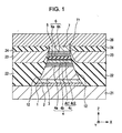
- Fig. 1 is a cross-sectional view of a tunnel type magnetic sensor (tunnel type magnetoresistive sensor) according to this embodiment of the present invention, taken along a face parallel to a facing face facing a recording medium.
- a tunnel type magnetic sensor is provided at a trailing side end portion or the like of a floating slider provided in a hard disk apparatus and detects a recorded magnetic field from a hard disk or the like.
- the tunnel type magnetic sensor is also used as a magnetoresistive memory (MRAM) or the like.
- an X direction indicates a track width direction
- a Y direction indicates a direction of a leak magnetic field from a magnetic recording medium (height direction)
- a Z direction indicates a traveling direction of a magnetic recording medium, such as a hard disk, and a lamination direction of layers forming the tunnel type magnetic sensor.
- a layer formed at the lowest position shown in Fig. 1 is a lower shield layer 21 formed, for example, from a NiFe alloy.
- a laminate T1 is formed on the lower shield layer 21.
- the tunnel type magnetic sensor described above includes, besides the laminate T1, lower insulating layers 22, hard bias layers 23, and upper insulating layers 24, which are formed at two sides of the laminate T1 in the track width direction (X direction in the figure).
- the lowest layer of the laminate T1 is an underlayer 1 formed of a non-magnetic material including at least one element selected from the group consisting of Ta, Hf, Nb, Zr, Ti, Mo, and W.
- a seed layer 2 is provided on this underlayer 1.
- the seed layer 2 is formed, for example, from NiFeCr.
- the seed layer 2 When the seed layer 2 is formed of NiFeCr, it has a face-centered cubic (fcc) structure in which equivalent crystalline planes represented by the ⁇ 111 ⁇ planes are preferentially oriented in a direction parallel to the surface of the film.
- the underlayer 1 may not be formed.
- An antiferromagnetic layer 3 formed on the seed layer 2 is preferably formed of an antiferromagnetic material containing an element ⁇ (where ⁇ is at least one element selected from the group consisting of Pt, Pd, Ir, Rh, Ru, and Os) and Mn.
- the ⁇ -Mn alloy using a platinum group element has superior corrosion resistance and a high blocking temperature, and in addition, as an antiferromagnetic material, this ⁇ -Mn alloy has superior properties such that an exchange coupling magnetic field (Hex) can be increased.
- Hex exchange coupling magnetic field
- the antiferromagnetic layer 3 may be formed of an antiferromagnetic material containing the element ⁇ , an element ⁇ ' (where ⁇ ' is at least one element selected from the group consisting of Ne, Ar, Kr, Xe, Be, B, C, N, Mg, A1, Si, P, Ti, V, Cr, Fe, Co, Ni, Cu, Zn, Ga, Ge, Zr, Nb, Mo, Ag, Cd, Sn, Hf, Ta, W, Re, Au, Pb, and rare earth elements), and Mn.
- ⁇ ' is at least one element selected from the group consisting of Ne, Ar, Kr, Xe, Be, B, C, N, Mg, A1, Si, P, Ti, V, Cr, Fe, Co, Ni, Cu, Zn, Ga, Ge, Zr, Nb, Mo, Ag, Cd, Sn, Hf, Ta, W, Re, Au, Pb, and rare earth elements
- a fixed magnetic layer 4 is formed on the antiferromagnetic layer 3.
- the fixed magnetic layer 4 has a laminated ferrimagnetic structure composed of a first fixed magnetic layer 4a, a non-magnetic interlayer 4b, and a second fixed magnetic layer 4c laminated to each other in that order from the bottom.
- PKAY interaction antiferromagnetic exchange coupling magnetic field
- This structure is a so-called laminated ferrimagnetic structure, and by this structure, the magnetization of the fixed magnetic layer 4 can be stabilized, and the exchange coupling magnetic field generated at the interface between the fixed magnetic layer 4 and the antiferromagnetic layer 3 can be apparently increased.
- the first fixed magnetic layer 4a and the second fixed magnetic layer 4c are formed, for example, to have a thickness of approximately 1.2 to 4.0 nm (12 to 40 ⁇ ), and the non-magnetic interlayer 4b is formed to have a thickness of approximately 0.8 to 1 nm (8 to 10 ⁇ ).
- the first fixed magnetic layer 4a is formed of a ferromagnetic material such as CoFe, NiFe, or CoFeNi.
- the non-magnetic interlayer 4b is formed of a non-magnetic conductive material such as Ru, Rh, Ir, Cr, Re, or Cu.
- the second fixed magnetic layer 4c is further composed of a CoFeB layer 4c1 formed of CoFeB and an interface layer 4c2 formed of CoFe or Co.
- An insulating barrier layer 5 formed on the fixed magnetic layer 4 is formed of Al-O (aluminum oxide).
- the insulating barrier layer 5 has a thickness of approximately 0.6 to 1.2 nm.
- a free magnetic layer 6 is formed on the insulating barrier layer 5.
- the free magnetic layer 6 is composed of a soft magnetic layer 6b formed of a magnetic material, such as a NiFe alloy, and an enhancing layer 6a formed of a CoFe alloy and provided between the soft magnetic layer 6b and the insulating barrier layer 5.
- the soft magnetic layer 6b is preferably formed of a magnetic material having superior soft magnetic properties
- the enhancing layer 6a is formed of a magnetic material having spin polarizability higher than that of the soft magnetic layer 6b.
- the free magnetic layer 6 may also have a laminated ferrimagnetic structure in which magnetic layers are laminated to each other with at least one non-magnetic interlayer provided therebetween.
- a track width Tw is determined by the width dimension of the free magnetic layer 6 in the track width direction (X direction in the figure).
- a protective layer 7 composed of Ta or the like is formed on the free magnetic layer 6.
- Two side end surfaces 12 of the laminate T1 in the track width direction are formed to be inclined surfaces so that the width dimension in the track width direction is gradually decreased from the lower side to the upper side.
- the lower shield layer 21 extending to the two sides of the laminate T1 and on the two side end surfaces 12 thereof, the lower insulating layers 22 are formed, the hard bias layers 23 are formed on the lower insulating layers 22, and in addition, on the hard bias layers 23, the upper insulating layers 24 are formed.
- a bias underlayer (not shown) may be formed between the lower insulating layer 22 and the hard bias layer 23.
- the bias underlayer is formed, for example, from Cr, W, or Ti.
- the insulating layers 22 and 24 are formed of an insulating material such as Al 2 O 3 or SiO 2 and insulate the top and the bottom of the hard bias layer 23 so as to suppress current flowing in a direction perpendicular to the interfaces between the individual layers of the laminate T1 from being shunted to the two sides of the laminate T1 in the track width direction.
- the hard bias layer 23 is formed, for example, of a Co-Pt (cobalt-platinum) alloy or a Co-Cr-Pt (cobalt-chromium-platinum) alloy.
- an upper shield layer 26 composed of a NiFe alloy or the like is formed.
- the lower shield layer 21 and the upper shield layer 26 function as electrode layers for the laminate T1, and in a direction perpendicular to the film surfaces of the layers forming the laminate T1 (in a direction parallel to the Z direction in the figure), current flows.
- the free magnetic layer 6 is magnetized in a direction parallel to the track width direction (X direction in the figure) by a bias magnetic field from the hard bias layers 23.
- the first fixed magnetic layer 4a and the second fixed magnetic layer 4c, which form the fixed magnetic layer 4 are magnetized in a direction parallel to the height direction (Y direction in the figure). Since the fixed magnetic layer 4 has a laminated ferrimagnetic structure, the first fixed magnetic layer 4a and the second fixed magnetic layer 4c are magnetized antiparallel to each other.
- the magnetization of the fixed magnetic layer 4 is fixed (the magnetization is not varied by an external magnetic field)
- the magnetization of the free magnetic layer 6 is varied by an external magnetic field.
- this principle it is designed that when the magnetization of the free magnetic layer 6 is varied by influence of an external magnetic field, the change in electrical resistance is grasped as the change in voltage, and a leak magnetic field from a recording medium is detected.
- the insulating barrier layer 5 is formed of Al-O (aluminum oxide).
- the second fixed magnetic layer 4c forming the fixed magnetic layer 4 provided under the insulating barrier layer 5 is formed to be in contact therewith and is composed of the CoFeB layer 4c1 formed of CoFeB and the interface layer 4c2 located between the CoFeB layer 4c1 and the insulating barrier layer 5 and formed of CoFe or Co.
- the interface layer 4c2 composed of CoFe or Co is provided between the CoFeB layer 4c1 and the insulating barrier layer 5 as is the case of this embodiment, since the concentration of the B element in the vicinity of the interface with the insulating barrier layer 5 is decreased to an appropriate level, the spin polarizability is improved, and in addition, since a sufficient planarization effect can be obtained by the CoFeB layer 4c1 which is likely to be placed in an amorphous state and which has a planarization effect due to the presence of the B element, the film quality of the insulating barrier layer 5 can be improved, so that a low RA and a high rate of change in resistance ( ⁇ R/R) can be simultaneously obtained.
- the CoFeB layer 4c1 is formed of ⁇ Co y Fe 1-y ⁇ 100-x B x (where y indicates (Co concentration in atomic percent ⁇ /(Co concentration + Fe concentration in atomic percent) and is hereinafter referred to as "atomic ratio"), and the B concentration x is preferably in the range of more than 16 to 40 atomic percent. It was found by the experiments to be described later that, as in the case in the past, when the second fixed magnetic layer 4c is formed to have a single CoFeB layer structure, and when the B concentration is set to approximately 16 atomic percent, the RA can be decreased and the rate of change in resistance ( ⁇ R/R) can be increased.
- the B concentration is increased to more than 16 atomic percent to facilitate the formation of an amorphous state, so that the flatness of the second fixed magnetic layer 4c is improved.
- B is not added to the interface layer 4c2 in contact with the insulating barrier layer 5 to decrease the B concentration in the vicinity of the interface with the insulating barrier layer 5 to an appropriate level, so that the spin polarizability is improved. Accordingly, compared to the results obtained in the past, in an effective manner, the RA can be decreased and the rate of change in resistance ( ⁇ R/R) can be increased at the same time. In addition, the variations in properties, that is, the RA and the rate of change in resistance ( ⁇ R/R), can be suppressed as compared to that in the past.
- the B concentration x is more preferably in the range of 17.5 to 35 atomic percent.
- B concentration x average thickness of the CoFeB layer
- the atomic ratio y of the CoFeB layer 4c1 and a Co concentration z of the interface layer 4c2 are preferably defined within a polyhedron in a three-dimensional graph shown in Fig. 10 surrounded by:
- the absolute thickness of the CoFeB layer 4c1 and the thickness ratio of the interface layer 4c2 to the CoFeB layer 4c1 which are optimum to simultaneously obtain a low RA and a high rate of change in resistance ( ⁇ R/R) are changed by the B concentration x.
- the B concentration x is in the range of 17.5 to 35 atomic percent, by controlling the average thickness of the CoFeB layer 4c1 and the thickness ratio of the interface layer 4c2 to the CoFeB layer 4c1 as described above, a low RA and a high rate of change in resistance ( ⁇ R/R) can be effectively obtained at the same time.
- the points E and I be connected by a line (including the line) and that the points K and O be connected by a line (including the line). That is, in the three-dimensional graph shown in Fig. 10, when the B concentration x is in the range of 17.5 to 35 atomic percent, the atomic ratio y of the CoFeB layer 4c1 and the Co concentration z of the interface layer 4c2 formed of Co z Fe 100-z are more preferably defined within a polyhedron surrounded by:
- the B concentration x is preferably in the range of 20 to 30 atomic percent.
- the atomic ratio y of the CoFeB layer and the Co concentration z of the interface layer formed of Co z fe 100-z are preferably defined within a polyhedron in the three-dimensional graph shown in Fig. 10 surrounded by:
- a low RA and a high rate of change in resistance ( ⁇ R/R) can be effectively obtained at the same time.
- the point e and the point i be connected to each other by a line (including the line) and that the point k and the point o be connected to each other by a line (including the line). That is, when the B concentration x is in the range of 20 to 30 atomic percent, the atomic ratio y of the CoFeB layer 4c1 and the Co concentration z of the interface layer 4c2 formed of Co z Fe 100-z are more preferably defined within a polyhedron of the three-dimensional graph shown in Fig.
- the total thickness of the second fixed magnetic layer 4c is preferably 4 nm or less.
- the average thickness of the second fixed magnetic layer 4c is preferably set to 4 nm at a maximum.
- an interlayer coupling magnetic field Hin caused by a topological magnetostatic coupling between the fixed magnetic layer 4 and the free magnetic layer 6 can be decreased by defining the average thickness of the CoFeB layer 4c1 as described above.
- the decrease in the interlayer coupling magnetic field Hin means that the flatness of the interface between the second fixed magnetic layer 4c and the insulating barrier layer 5 is improved.
- a low RA can be obtained as described above. Since being a very important value for optimization of high-speed data transfer, an increase in high-recording density, and the like, the RA must be set to a small value.
- the RA can be set to a small value as compared to that in the past.
- the RA can be set to less than 5.8 ⁇ m 2 which is a value of a related example, and in particular, the RA can be decreased from that of the related example by approximately 0.4 to 0.8 ⁇ m 2 .
- an annealing treatment (heat treatment) is performed in a manufacturing process, as described below.
- the annealing treatment is performed, for example, at a temperature of approximately 240 to 310°C.
- This annealing treatment is, for example, an annealing treatment in a magnetic field in which an exchange coupling magnetic field (Hex) is generated between the antiferromagnetic layer 3 and the first fixed magnetic layer 4a forming the fixed magnetic layer 4.
- Hex exchange coupling magnetic field
- the temperature of the annealing treatment is less than 240°C, or when the annealing time is less than 1 hour even at a temperature in the range of 240 to 310°C, no counter diffusion of constituent elements occurs at the interface between the interface layer 4c2 and the CoFeB layer 4c1, or even if the counter diffusion occurs, the degree thereof is not significant (for example, diffusion does not occur at the entire interface but only intermittently occurs), and it is believed that the state of the interface is practically maintained.
- the temperature of the annealing treatment is more than 310°C, or when the annealing time is 1 hour or more and the annealing temperature is in the range of 240 to 310°C, counter diffusion of constituent elements occurs at the interface between the interface layer 4c2 and the CoFeB layer 4c1, as shown in Fig. 2 or 3, and the interface described above disappears; hence, it is believed that the composition gradient region of the B concentration is formed.
- the second fixed magnetic layer 4c is composed of a CoFeB region 10 formed of CoFeB and an intervening region 11 which is formed of CoFe or Co and which is located between the CoFeB region 10 and the insulating barrier layer 5.
- B is not contained in the intervening region 11.
- the CoFeB region 10 in the CoFeB region 10, there is a composition gradient region in which the B concentration gradually decreases from a lower surface side (side at the interface in contact with the non-magnetic interlayer 4b) toward the intervening region 11.
- the B concentration decreases as compared to that at the inner side, and the reason for this decrease is the element diffusion with the non-magnetic interlayer 4b.
- the second fixed magnetic layer 4c is entirely formed of CoFeB
- the B concentration at an upper surface side in contact with the insulating barrier layer 5 is lower than that at a lower surface side in contact with the non-magnetic interlayer 4b.
- the B concentration decreases as compared to that at the inner side, and the reason for this decrease is the element diffusion with the non-magnetic interlayer 4b.
- the fixed magnetic layer 4 has a laminated ferrimagnetic structure including the first fixed magnetic layer 4a, the non-magnetic interlayer 4b, and the second fixed magnetic layer 4c; however, for example, even when the fixed magnetic layer 4 is formed of a single layer or has a laminated structure including a plurality of magnetic layers, this embodiment can be applied thereto.
- the fixed magnetic layer 4 has a laminated ferrimagnetic structure, as described above, since the magnetization of the fixed magnetic layer 4 can be more appropriately fixed, improvement in reproduction output can be preferably performed.
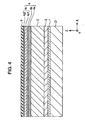
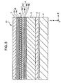
- FIGs. 4 to 7 are partial cross-sectional views each showing a tunnel type magnetic sensor in process taken along the same direction as that shown in Fig. 1.
- the underlayer 1, the seed layer 2, the antiferromagnetic layer 3, the first fixed magnetic layer 4a, the non-magnetic interlayer 4b, and the second fixed magnetic layer 4c are sequentially formed.
- the individual layers are formed by sputtering.
- the second fixed magnetic layer 4c are formed by laminating the CoFeB layer 4c1 formed of CoFeB and the interface layer 4c2 formed of CoFe or Co in that order from the bottom.
- the CoFeB layer 4c1 is preferably formed of (Co 1-y Fe y ) 100-x B x and the B concentration x is preferably set in the range of more than 16 to 40 atomic percent.
- the B concentration x is more preferably set in the range of 17.5 to 35 atomic percent.
- B concentration x average thickness of the CoFeB layer
- the B concentration x is formed in the range of 17.5 to 35 atomic percent
- the atomic ratio y of the CoFeB layer 4c1 and the Co concentration z of the interface layer 4c2 formed of Co z Fe 100-z are preferably adjusted within a polyhedron in the three-dimensional graph shown in Fig. 10 surrounded by:
- the B concentration x is preferably formed in the range of 20 to 30 atomic percent.
- B concentration x average thickness of the CoFeB layer 4c1
- the atomic ratio y of the CoFeB layer 4c1 and the Co concentration z of the interface layer 4c2 formed of Co z Fe 100-z are preferably adjusted within a polyhedron in the three-dimensional graph shown in Fig. 10 surrounded by:
- a plasma treatment is performed on the surface of the second fixed magnetic layer 4c.
- the above plasma treatment is performed to improve the flatness of the surface of the second fixed magnetic layer 4c; however, in the structure in which the interface layer 4c2 having a small thickness is provided on the CoFeB layer 4c1 having superior flatness as is the case of this embodiment, since the flatness of the surface of the second fixed magnetic layer 4c is originally superior, whether the plasma treatment is performed or not may be optionally determined.
- the insulating barrier layer 5 composed of Al-O is formed on the second fixed magnetic layer 4c.
- an Al layer is formed on the second fixed magnetic layer 4c by sputtering, followed by oxidation of the Al layer, so that the insulating barrier layer 5 composed of Al-O is formed.
- an oxidation method for example, radical oxidation, ion oxidation, plasma oxidation, or natural oxidation may be mentioned.
- the Al layer is formed to have a thickness of approximately 0.2 to 0.6 nm.
- the insulating barrier layer 5 composed of Al-O may be directly formed, for example, by an RF sputtering method using a target of Al-O.
- the free magnetic layer 6, which is composed of the enhancing layer 6a and the soft magnetic layer 6b, and the protective layer 7 are formed.
- the enhancing layer 6a is preferably formed of CoFe having an Fe composition ratio of 5 to 90 atomic percent.
- the soft magnetic layer 6b is preferably formed of an NiFe alloy having a Ni composition ratio of 78 to 96 atomic percent.
- the laminate T1 containing from the underlayer 1 to the protective layer 7 laminated to each other is formed.
- a lift-off resist layer 30 is formed, and two side end portions of the laminate T1 in the track width direction (X direction in the figure), which are not covered with the lift-off resist layer 30, are removed by etching or the like (see Fig. 6).
- the lower insulating layers 22, the hard bias layers 23, and the upper insulating layers 24 are laminated in that order from the bottom (see Fig. 7).
- the lift-off resist layer 30 is removed, and the upper shield layer 26 is formed on the laminate T1 and the upper insulating layers 24.
- an annealing treatment is performed in the manufacturing process.
- an annealing treatment to generate an exchange coupling magnetic field (Hex) between the antiferromagnetic layer 3 and the first fixed magnetic layer 4a may be mentioned.
- the temperature of the annealing treatment is less than 240°C, or when the annealing time is less than 1 hour even at a temperature in the range of 240 to 310°C, no counter diffusion of constituent elements occurs at interfaces between the layers, or even if the counter diffusion occurs, the degree thereof is not significant (for example, diffusion does not occur at the entire interface but only intermittently occurs), and it is believed that the state of the interface is practically maintained.
- the temperature of the annealing treatment is more than 310°C, or when the annealing time is 1 hour or more and the annealing temperature is in the range of 240 to 310°C, it is believed that counter diffusion of constituent elements occurs at the interfaces between the layers.
- the counter diffusion as described above, it is believed that as shown in Figs. 2 and 3, the interface between the CoFeB layer 4c1 and the interface layer 4c2 disappears inside the second fixed magnetic layer 4c so that the composition gradient region of the B concentration is formed.
- a low RA element resistance R ⁇ element area A
- a high rate of change in resistance ⁇ R/R
- the second fixed magnetic layer 4c is formed of a single CoFeB layer by adjusting a material for and a thickness ratio of the second fixed magnetic layer 4c as described above, or to the reference example in which the CoFeB layer 4c1 and the interface layer 4c2, which form the second fixed magnetic layer 4c, are laminated in reverse order.
- a low RA and a high rate of change in resistance ( ⁇ R/R) can be effectively obtained at the same time.
- the variations in properties, such as the RA and the rate of change in resistance ( ⁇ R/R) can be effectively suppressed.
- a method may also be performed having the steps of preparing a plurality of Co-Fe-B targets having different B concentrations, and performing sputtering to form the second fixed magnetic layer 4c while the targets are being changed so as to gradually decrease the B concentration.
- the value in the parentheses indicates the average thickness, and the unit thereof is nm.
- the surface of the second fixed magnetic layer 4c was processed by a plasma treatment before the insulating barrier layer 5 was formed.
- the second fixed magnetic layer 4c there were formed a single layer structure 1 (related example) composed of (Co 0.75 Fe 0.25 ) 100-x B x (t1), a laminated structure 1 containing (Co 0.75 Fe 0.25 ) 100-x B x (t1) and Co 75at% Fe 25at% (t2) laminated in that order from the bottom, and a laminated structure 2 (lamination structure described in the above Japanese Unexamined Patent Application Publications; reference example) containing Co 75at% Fe 25at% (t2) and (CO 0.75 Fe 0.25 ) 100-x B x (t1) laminated in that order from the bottom.
- a laminated structure 2 laminated structure described in the above Japanese Unexamined Patent Application Publications; reference example
- the B concentration x was represented by atomic percent.
- the average thicknesses t1 and t2 were represented by nm, and the total thickness of the second fixed magnetic layer 4c was adjusted to be 1.8 nm.
- the laminates used in the above experiment were each in the form of a solid film, in the following experiment, the same laminates as those described above (however, samples were included in which the first fixed magnetic layer 4a and/or the second fixed magnetic layer 4c had a different thickness) were each machined to have the shape of the tunnel type magnetic sensor shown in Fig. 1, and the variations in RA and rate of change in resistance ( ⁇ R/R) were measured.
- one tunnel type magnetic sensor having a B concentration x of 16 atomic percent was selected among the single layer structures 1 (related examples) shown in Table 1, three types of tunnel type magnetic sensors were selected among the laminated structures 1, each having a B concentration x of 20 atomic percent and a different average thickness (t1) of the CoFeB layer 4c1 or the like, and three types of tunnel type magnetic sensors were selected among the laminated structures 1, each having a B concentration x of 30 atomic percent and a different average thickness (t1) of the CoFeB layer 4c1 or the like. Subsequently, 80 tunnel type magnetic sensors of each type described above were manufactured, and the average of the RA, the average of the rate of change in resistance ( ⁇ R/R), and the variations thereof were measured.
- the track width Tw and the height length of each sensor were set to 0.085 ⁇ m and 0.4 ⁇ m, respectively.
- the variations in properties were represented by ( ⁇ /Ave (%)).
- ⁇ indicates the standard deviation
- Ave indicates the average of the RA and that of the rate of change in resistance ( ⁇ R/R).
- samples of the examples in which the second fixed magnetic layer 4c was formed of CoFeB 20at% and CoFe provided in that order from the bottom were further additionally formed as described below, and the RA and the rate of change in resistance ( ⁇ R/R) were also measured.
- the laminate T1 of the tunnel type magnetic sensor shown in Fig. 1 was formed by laminating the underlayer 1 of Ta (3); the seed layer 2 of (Ni 0.8 Fe 0.2 ) 60at% Cr 40at% (5); the antiferromagnetic layer 3 of IrMn (7); the fixed magnetic layer 4 composed of the first fixed magnetic layer 4a of Co 70at% Fe 30at% (1.4), the non-magnetic interlayer 4b of Ru (0.9), and the second fixed magnetic layer 4c (1.8); the insulating barrier layer 5 of Al-O; the free magnetic layer 6 composed of the enhancing layer 6a of Co 50at% Fe 50at% (1), and the soft magnetic layer 6b of Ni 84at% Fe 16at% (5); and the protective layer 7 of Ru(1)/Ta(28) in that order from the bottom.
- the value in the parentheses indicates the average thickness, and the unit thereof is nm.
- the surface of the second fixed magnetic layer 4c was processed by a plasma treatment before the insulating barrier layer 5 was formed.
- the values in the parentheses of the individual structures indicate the thicknesses, and the unit thereof is nm.
- the second fixed magnetic layer 4c was formed by laminating the CoFeB layer 4c1 and the interface layer 4c2 of CoFe or Co in that order from the bottom, and in addition, the B concentration x was set in the range of more than 16 to 40 atomic percent. In addition, a more preferable B concentration x was set in the range of 17.5 to 35 atomic percent, and the most preferable B concentration x was set in the range of 20 to 30 atomic percent.
- the value in the parentheses indicates the average thickness, and the unit thereof is nm.
- the surface of the second fixed magnetic layer 4c was processed by a plasma treatment before the insulating barrier layer 5 was formed.
- the above laminate was in the form of a solid film.
- the value in the parentheses indicates the average thickness, and the unit thereof is nm.
- the surface of the second fixed magnetic layer 4c was processed by a plasma treatment before the insulating barrier layer 5 was formed.
- the above laminate was in the form of a solid film.
- the thickness ratio (t2/t1) was preferably set in the range of 0.1 to 0.6.
- the thickness ratio (t2/t1) was preferably set in the range of 0.5 to 1.3.
- Fig. 8 is the graph showing the relationship between the B concentration x and the average thickness t1 of the CoFeB layer 4c1.
- the point (3) shown in Fig. 8 indicates a minimum necessary thickness (1.5 nm) of the CoFeB layer 4c1 when the B concentration x is set to 20 atomic percent
- the point (4) indicates a minimum necessary thickness (0.9 nm) of the CoFeB layer 4c1 when the B concentration x is set to 30 atomic percent.
- the points (1) and (2) are obtained by extending the line that runs on the points (3) and (4).
- Fig. 9 shows the relationship between the B concentration x and the thickness ratio (t2/t1) of the interface layer 4c2 to the CoFeB layer 4c1.
- the point a shown in Fig. 9 indicates a minimum thickness ratio (t2/t1) (0.10) when the B concentration x is set to 20 atomic percent
- the point b indicates a minimum thickness ratio (t2/t1) (0.50) when the B concentration x is set to 30 atomic percent
- the point c indicates a maximum thickness ratio (t2/t1) (1.30) when the B concentration x is set to 30 atomic percent
- the point d indicates a maximum thickness ratio (t2/t1) (0.60) when the B concentration x is set to 20 atomic percent.
- the points A and B are obtained by extending the line that runs on the points a and b
- the points C and D are obtained by extending the line that runs on the points c and d.
- the B concentration x, the necessary average thickness (t1) of the CoFeB layer 4c1, and the minimum and the maximum thickness ratios (t2/t1) are shown in Table 10 below.
- Table 10 B concentration (at.%) Necessary CoFeB thickness t1(nm) Ratio of CoFe thickness to CoFeB thickness Minimum Maximum 17.5 1.65 0.00 (A) 0.43 (D) 20 1.50 0.10 (a) 0.60 (d) 30 0.90 0.50 (b) 1.30 (c) 35 0.60 0.70 (B) 1.65 (C)
- the average thickness t1 of the CoFeB layer 4c1 is set in the range of a line and thereabove in the graph (including the line) shown in Fig. 8, the line that runs on the points (1) and (2) in the graph.
- the thickness ratio (t2/t1) is set in the range surrounded by the line that runs on the points A and B (including the line, however, the point A is excluded), the line that runs on the points B and C (including the line, however), the line that runs on the points C and D (including the line), and the line that runs on the points D and A (including the line, however, the point A is excluded).
- the B concentration x is set in the range of 17.5 to 35 atomic percent, a low RA and a high rate of change in resistance ( ⁇ R/R) can be effectively obtained at the same time.
- the average thickness t1 of the CoFeB layer 4c1 is set in the range of a line and thereabove in the graph (including the line) shown in Fig. 8, the line that runs on the points (3) and (4) in the graph.
- the thickness ratio (t2/t1) is set in the range surrounded by the line that runs on the points a and b (including the line), the line that runs on the points b and c (including the line), the line that runs on the points c and d (including the line), and the line that runs on the points d and a (including the line).
- the B concentration x is set in the range of 20 to 30 atomic percent, a low RA and a high rate of change in resistance ( ⁇ R/R) can be effectively obtained at the same time.
- the value in the parentheses indicates the average thickness, and the unit thereof is nm.
- An A1 layer having a thickness of 0.43 nm was formed, followed by oxidation thereof, so that the insulating barrier layer 5 was formed.
- the surface of the second fixed magnetic layer 4c was processed by a plasma treatment before the insulating barrier layer 5 was formed.
- the above laminate was in the form of a solid film.
- the B concentration x was set in the range of 20 to 30 atomic percent, and in addition, as shown in Table 11 below, by adjusting the average thickness t1 of the CoFeB layer 4c1 and the average thickness t2 of the interface layer (CoFe) 4c2, the interlayer coupling magnetic field Hin of each sample was measured.
- Table 11 Second fixed magnetic layer CoFeB B concentration (at.
- the interlayer coupling magnetic field Hin increases when the thickness of the second fixed magnetic layer is increased so as to increase the magnetization; however, as shown in Table 11, when the B concentration x was set to 20 atomic percent, the Hin was minimized when the average thickness t1 of the CoFeB layer was 1.5 nm, and when the B concentration x was set to 30 atomic percent, the Hin was minimized when the average thickness t1 of the CoFeB layer was 0.9 nm.
- the value in the parentheses indicates the average thickness, and the unit thereof is nm.
- the surface of the second fixed magnetic layer 4c was processed by a plasma treatment before the insulating barrier layer 5 was formed.
- the value in the parentheses indicates the average thickness, and the unit thereof is nm.
- the surface of the second fixed magnetic layer 4c was processed by a plasma treatment before the insulating barrier layer 5 was formed.
- Fig. 10 is a three-dimensional graph in which an X axis indicates the atomic ratio y, a Y axis indicates the Co concentration z, and a Z axis indicates the B concentration x.
- the points shown in Fig. 10 are measurement points shown in Tables 12 and 13.
- the points E and K are obtained by extending a line that runs on the points e and k.
- the points F and L are obtained by extending a line that runs on the points f and 1.
- the points G and M are obtained by extending a line that runs on the points g and m.
- the points H and N are obtained by extending a line that runs on the points h and n.
- the points I and O are obtained by extending a line that runs on the points i and o.
- the points J and P are obtained by extending a line that runs on the points j and p.
- the atomic ratio y and the Co concentration z are defined within a polyhedron in the three-dimensional graph shown in Fig. 10 surrounded by:
- the points E and I be connected by a line (including the line) and that the points K and O be connected by a line (including the line). That is, when the B concentration x is set in the range of 17.5 to 35 atomic percent, the atomic ratio y and the Co concentration z are more preferably defined within a polyhedron in the three-dimensional graph shown in Fig. 10 surrounded by:
- the atomic ratio y and the Co concentration z were defined in a polyhedron surrounded by a line (including the line) that runs on the points e and f, a line (including the line) that runs on the points f and g, a line (including the line) that runs on the points g and h, a line (including the line) that runs on the points h and i, a line (including the line) that runs on the points i and j, and a line (including the line) that runs on the points j and e;
- the point e and the point i be connected by a line (including the line), and the point k and the point o be connected by a line (including the line). That is, when the B concentration x is in the range of 20 to 30 atomic percent, the atomic ratio y of the CoFeB layer 4c1 and the Co concentration z of the interface layer 4c2 formed of Co z Fe 100-z are more preferably defined within a polyhedron shown in the three-dimensional graph in Fig. 10 surrounded by:
Landscapes
- Engineering & Computer Science (AREA)
- Chemical & Material Sciences (AREA)
- Nanotechnology (AREA)
- Crystallography & Structural Chemistry (AREA)
- Physics & Mathematics (AREA)
- Manufacturing & Machinery (AREA)
- Power Engineering (AREA)
- Condensed Matter Physics & Semiconductors (AREA)
- General Physics & Mathematics (AREA)
- Spectroscopy & Molecular Physics (AREA)
- Computer Hardware Design (AREA)
- Mathematical Physics (AREA)
- Theoretical Computer Science (AREA)
- Hall/Mr Elements (AREA)
- Measuring Magnetic Variables (AREA)
- Magnetic Heads (AREA)
- Mram Or Spin Memory Techniques (AREA)
- Thin Magnetic Films (AREA)
Applications Claiming Priority (2)
| Application Number | Priority Date | Filing Date | Title |
|---|---|---|---|
| JP2006255646 | 2006-09-21 | ||
| JP2007065657A JP2008103662A (ja) | 2006-09-21 | 2007-03-14 | トンネル型磁気検出素子及びその製造方法 |
Publications (2)
| Publication Number | Publication Date |
|---|---|
| EP1903623A2 true EP1903623A2 (de) | 2008-03-26 |
| EP1903623A3 EP1903623A3 (de) | 2011-12-21 |
Family
ID=38896926
Family Applications (1)
| Application Number | Title | Priority Date | Filing Date |
|---|---|---|---|
| EP07018079A Withdrawn EP1903623A3 (de) | 2006-09-21 | 2007-09-14 | Tunnelmagnetsensor mit fixierter magnetischer Schicht aus einer Verbundwerkstoffstruktur mit einer CoFeB-Schicht und Verfahren zu seiner Herstellung |
Country Status (3)
| Country | Link |
|---|---|
| US (1) | US20080174921A1 (de) |
| EP (1) | EP1903623A3 (de) |
| JP (1) | JP2008103662A (de) |
Cited By (2)
| Publication number | Priority date | Publication date | Assignee | Title |
|---|---|---|---|---|
| WO2017015294A1 (en) * | 2015-07-20 | 2017-01-26 | Headway Technologies, Inc. | Magnetic tunnel junction with low defect rate after high temperature anneal for magnetic device applications |
| US11462681B2 (en) * | 2018-06-19 | 2022-10-04 | Sony Semiconductor Solutions Corporation | Magnetic storage element, magnetic head, magnetic storage device, electronic apparatus, and method for manufacturing magnetic storage element |
Families Citing this family (16)
| Publication number | Priority date | Publication date | Assignee | Title |
|---|---|---|---|---|
| US7695761B1 (en) | 2006-12-21 | 2010-04-13 | Western Digital (Fremont), Llc | Method and system for providing a spin tunneling magnetic element having a crystalline barrier layer |
| US8623452B2 (en) * | 2010-12-10 | 2014-01-07 | Avalanche Technology, Inc. | Magnetic random access memory (MRAM) with enhanced magnetic stiffness and method of making same |
| US8559141B1 (en) | 2007-05-07 | 2013-10-15 | Western Digital (Fremont), Llc | Spin tunneling magnetic element promoting free layer crystal growth from a barrier layer interface |
| US8545999B1 (en) * | 2008-02-21 | 2013-10-01 | Western Digital (Fremont), Llc | Method and system for providing a magnetoresistive structure |
| WO2010026667A1 (en) | 2008-09-03 | 2010-03-11 | Canon Anelva Corporation | Ferromagnetic preferred grain growth promotion seed layer for amorphous or microcrystalline mgo tunnel barrier |
| JP2010062353A (ja) * | 2008-09-04 | 2010-03-18 | Fujitsu Ltd | 磁気抵抗効果素子 |
| US9040178B2 (en) * | 2008-09-22 | 2015-05-26 | Headway Technologies, Inc. | TMR device with novel free layer structure |
| WO2010044134A1 (ja) * | 2008-10-14 | 2010-04-22 | キヤノンアネルバ株式会社 | 磁気抵抗効果素子の製造方法及び磁気抵抗効果素子製造プログラム |
| KR101584747B1 (ko) | 2009-01-20 | 2016-01-13 | 삼성전자주식회사 | 자기 메모리 소자 |
| US8498084B1 (en) | 2009-07-21 | 2013-07-30 | Western Digital (Fremont), Llc | Magnetoresistive sensors having an improved free layer |
| JP5588642B2 (ja) * | 2009-09-02 | 2014-09-10 | エイチジーエスティーネザーランドビーブイ | トンネル接合型磁気抵抗効果ヘッド及びその製造方法 |
| US8194365B1 (en) | 2009-09-03 | 2012-06-05 | Western Digital (Fremont), Llc | Method and system for providing a read sensor having a low magnetostriction free layer |
| US20110236723A1 (en) * | 2010-03-26 | 2011-09-29 | Tsann Lin | CURRENT-PERPENDICULAR-TO-PLANE (CPP) READ SENSOR WITH Co-Fe BUFFER LAYERS |
| SG11201504875UA (en) | 2012-12-20 | 2015-07-30 | Canon Anelva Corp | Method for manufacturing magnetoresistance effect element |
| US9070381B1 (en) | 2013-04-12 | 2015-06-30 | Western Digital (Fremont), Llc | Magnetic recording read transducer having a laminated free layer |
| EP3979345B1 (de) | 2017-11-29 | 2023-11-01 | Everspin Technologies, Inc. | Magnetoresistiver stapel |
Family Cites Families (6)
| Publication number | Priority date | Publication date | Assignee | Title |
|---|---|---|---|---|
| US6436526B1 (en) * | 1999-06-17 | 2002-08-20 | Matsushita Electric Industrial Co., Ltd. | Magneto-resistance effect element, magneto-resistance effect memory cell, MRAM and method for performing information write to or read from the magneto-resistance effect memory cell |
| US7098495B2 (en) * | 2004-07-26 | 2006-08-29 | Freescale Semiconducor, Inc. | Magnetic tunnel junction element structures and methods for fabricating the same |
| US7800868B2 (en) * | 2005-12-16 | 2010-09-21 | Seagate Technology Llc | Magnetic sensing device including a sense enhancing layer |
| US7821747B2 (en) * | 2006-02-10 | 2010-10-26 | Hitachi Global Storage Technologies Netherlands B.V. | Method and apparatus for providing improved pinning structure for tunneling magnetoresistive sensor |
| US7760474B1 (en) * | 2006-07-14 | 2010-07-20 | Grandis, Inc. | Magnetic element utilizing free layer engineering |
| US7764468B2 (en) * | 2007-04-16 | 2010-07-27 | Tdk Corporation | Method for removing smear and magnetic recording/reproducing apparatus with function of removing smear |
-
2007
- 2007-03-14 JP JP2007065657A patent/JP2008103662A/ja active Pending
- 2007-09-14 EP EP07018079A patent/EP1903623A3/de not_active Withdrawn
- 2007-09-21 US US11/859,412 patent/US20080174921A1/en not_active Abandoned
Cited By (6)
| Publication number | Priority date | Publication date | Assignee | Title |
|---|---|---|---|---|
| WO2017015294A1 (en) * | 2015-07-20 | 2017-01-26 | Headway Technologies, Inc. | Magnetic tunnel junction with low defect rate after high temperature anneal for magnetic device applications |
| US9842988B2 (en) | 2015-07-20 | 2017-12-12 | Headway Technologies, Inc. | Magnetic tunnel junction with low defect rate after high temperature anneal for magnetic device applications |
| US10763428B2 (en) | 2015-07-20 | 2020-09-01 | Taiwan Semiconductor Manufacturing Company, Ltd. | Magnetic tunnel junction with low defect rate after high temperature anneal for magnetic device applications |
| US11309489B2 (en) | 2015-07-20 | 2022-04-19 | Taiwan Semiconductor Manufacturing Company, Ltd. | Magnetic tunnel junction with low defect rate after high temperature anneal for magnetic device applications |
| US12167701B2 (en) | 2015-07-20 | 2024-12-10 | Taiwan Semiconductor Manufacturing Company, Ltd. | Magnetic tunnel junction with low defect rate after high temperature anneal for magnetic device applications |
| US11462681B2 (en) * | 2018-06-19 | 2022-10-04 | Sony Semiconductor Solutions Corporation | Magnetic storage element, magnetic head, magnetic storage device, electronic apparatus, and method for manufacturing magnetic storage element |
Also Published As
| Publication number | Publication date |
|---|---|
| JP2008103662A (ja) | 2008-05-01 |
| EP1903623A3 (de) | 2011-12-21 |
| US20080174921A1 (en) | 2008-07-24 |
Similar Documents
| Publication | Publication Date | Title |
|---|---|---|
| EP1903623A2 (de) | Tunnelmagnetsensor mit fixierter magnetischer Schicht aus einer Verbundwerkstoffstruktur mit einer CoFeB-Schicht und Verfahren zu seiner Herstellung | |
| CN101101959B (zh) | 磁阻效应元件的制造方法 | |
| EP1903624B1 (de) | Magnetoresistiver Tunnelsensor, indem mindestens ein Teil der Pinningschicht aus einer CoFeB-Schicht zusammengesetzt ist, und Verfahren zur Herstellung des magnetoresistiven Tunnelsensors | |
| JP4786331B2 (ja) | 磁気抵抗効果素子の製造方法 | |
| US9028909B2 (en) | Magnetoresistive element and method of manufacturing the same | |
| CN100557840C (zh) | CoFeB层构成固定层至少一部分的隧道型磁检测元件及其制法 | |
| US7365948B2 (en) | Exchange-coupled film, method for making exchange-coupled film, and magnetic sensing element including exchange-coupled film | |
| US8446698B2 (en) | Magnetoresistive element, magnetic head assembly, and magnetic recording/reproducing apparatus | |
| US20080151438A1 (en) | Magnetoresistive element | |
| US8009391B2 (en) | Magnetic sensing element and method for manufacturing the same | |
| US7898776B2 (en) | Tunneling magnetic sensing element including enhancing layer having high Fe concentration in the vicinity of barrier layer | |
| JP3908557B2 (ja) | 磁気検出素子の製造方法 | |
| US20120192998A1 (en) | Method of manufacturing a magneto-resistance effect element | |
| US20080186639A1 (en) | Tunneling magnetic sensing element and method for producing same | |
| JP2003086861A (ja) | 磁気検出素子及びその製造方法 | |
| US6891703B2 (en) | Exchange coupled film having magnetic layer with non-uniform composition and magnetic sensing element including the same | |
| US8130476B2 (en) | Tunneling magnetic sensing element and method for manufacturing the same | |
| CN100412950C (zh) | 磁盘装置 | |
| US7961442B2 (en) | Tunneling magnetic detecting element having insulation barrier layer and method for making the same | |
| US7643254B2 (en) | Tunnel-effect type magnetic sensor having free layer including non-magnetic metal layer | |
| US20080055786A1 (en) | Tunnel type magnetic sensor having protective layer formed from Pt or Ru on free magnetic layer, and method for manufacturing the same | |
| US20080160326A1 (en) | Tunneling magnetic sensing element and method for manufacturing the same | |
| US20080286612A1 (en) | Tunneling magnetic sensing element including Pt sublayer disposed between free magnetic sublayer and enhancing sublayer and method for producing tunneling magnetic sensing element |
Legal Events
| Date | Code | Title | Description |
|---|---|---|---|
| PUAI | Public reference made under article 153(3) epc to a published international application that has entered the european phase |
Free format text: ORIGINAL CODE: 0009012 |
|
| AK | Designated contracting states |
Kind code of ref document: A2 Designated state(s): AT BE BG CH CY CZ DE DK EE ES FI FR GB GR HU IE IS IT LI LT LU LV MC MT NL PL PT RO SE SI SK TR |
|
| AX | Request for extension of the european patent |
Extension state: AL BA HR MK YU |
|
| PUAL | Search report despatched |
Free format text: ORIGINAL CODE: 0009013 |
|
| AK | Designated contracting states |
Kind code of ref document: A3 Designated state(s): AT BE BG CH CY CZ DE DK EE ES FI FR GB GR HU IE IS IT LI LT LU LV MC MT NL PL PT RO SE SI SK TR |
|
| AX | Request for extension of the european patent |
Extension state: AL BA HR MK RS |
|
| RIC1 | Information provided on ipc code assigned before grant |
Ipc: G01R 33/09 20060101ALI20111111BHEP Ipc: H01L 43/12 20060101ALI20111111BHEP Ipc: H01L 43/08 20060101AFI20111111BHEP |
|
| AKY | No designation fees paid | ||
| REG | Reference to a national code |
Ref country code: DE Ref legal event code: R108 |
|
| REG | Reference to a national code |
Ref country code: DE Ref legal event code: R108 Effective date: 20120829 |
|
| STAA | Information on the status of an ep patent application or granted ep patent |
Free format text: STATUS: THE APPLICATION IS DEEMED TO BE WITHDRAWN |
|
| 18D | Application deemed to be withdrawn |
Effective date: 20120622 |