EP1903624B1 - Détecteur magnéto-résistant à tunnel dans lequel au moins une partie de la couche d'ancrage est composée d'une couche CoFeB et procédé de fabrication du détecteur magnéto-résistant à tunnel - Google Patents
Détecteur magnéto-résistant à tunnel dans lequel au moins une partie de la couche d'ancrage est composée d'une couche CoFeB et procédé de fabrication du détecteur magnéto-résistant à tunnel Download PDFInfo
- Publication number
- EP1903624B1 EP1903624B1 EP07018080A EP07018080A EP1903624B1 EP 1903624 B1 EP1903624 B1 EP 1903624B1 EP 07018080 A EP07018080 A EP 07018080A EP 07018080 A EP07018080 A EP 07018080A EP 1903624 B1 EP1903624 B1 EP 1903624B1
- Authority
- EP
- European Patent Office
- Prior art keywords
- magnetic
- layer
- subsublayer
- insulating barrier
- sublayer
- Prior art date
- Legal status (The legal status is an assumption and is not a legal conclusion. Google has not performed a legal analysis and makes no representation as to the accuracy of the status listed.)
- Not-in-force
Links
- 238000004519 manufacturing process Methods 0.000 title claims description 29
- 229910019236 CoFeB Inorganic materials 0.000 title claims description 27
- 238000000034 method Methods 0.000 title claims description 27
- 230000005291 magnetic effect Effects 0.000 claims description 414
- 230000004888 barrier function Effects 0.000 claims description 103
- 230000005415 magnetization Effects 0.000 claims description 36
- 239000000203 mixture Substances 0.000 claims description 35
- 229910003321 CoFe Inorganic materials 0.000 claims description 25
- 238000000137 annealing Methods 0.000 claims description 14
- 239000013078 crystal Substances 0.000 claims description 14
- 229910045601 alloy Inorganic materials 0.000 claims description 10
- 239000000956 alloy Substances 0.000 claims description 10
- 230000015572 biosynthetic process Effects 0.000 claims description 10
- 238000009792 diffusion process Methods 0.000 claims description 8
- 229910001030 Iron–nickel alloy Inorganic materials 0.000 claims description 7
- 230000007423 decrease Effects 0.000 claims description 6
- 229910019092 Mg-O Inorganic materials 0.000 claims 7
- 229910019395 Mg—O Inorganic materials 0.000 claims 7
- 239000010410 layer Substances 0.000 description 259
- 230000008859 change Effects 0.000 description 54
- 239000000395 magnesium oxide Substances 0.000 description 29
- CPLXHLVBOLITMK-UHFFFAOYSA-N magnesium oxide Inorganic materials [Mg]=O CPLXHLVBOLITMK-UHFFFAOYSA-N 0.000 description 29
- AXZKOIWUVFPNLO-UHFFFAOYSA-N magnesium;oxygen(2-) Chemical compound [O-2].[Mg+2] AXZKOIWUVFPNLO-UHFFFAOYSA-N 0.000 description 29
- 230000005290 antiferromagnetic effect Effects 0.000 description 14
- 230000000052 comparative effect Effects 0.000 description 11
- 239000011777 magnesium Substances 0.000 description 8
- 238000009812 interlayer coupling reaction Methods 0.000 description 7
- 239000002356 single layer Substances 0.000 description 7
- 230000008878 coupling Effects 0.000 description 6
- 238000010168 coupling process Methods 0.000 description 6
- 238000005859 coupling reaction Methods 0.000 description 6
- 238000002474 experimental method Methods 0.000 description 6
- 239000000463 material Substances 0.000 description 6
- 230000008569 process Effects 0.000 description 6
- 239000011241 protective layer Substances 0.000 description 5
- 230000005641 tunneling Effects 0.000 description 5
- 238000010438 heat treatment Methods 0.000 description 4
- 230000003647 oxidation Effects 0.000 description 4
- 238000007254 oxidation reaction Methods 0.000 description 4
- 239000002885 antiferromagnetic material Substances 0.000 description 3
- 229910052799 carbon Inorganic materials 0.000 description 3
- 229910052804 chromium Inorganic materials 0.000 description 3
- 230000000694 effects Effects 0.000 description 3
- 239000000696 magnetic material Substances 0.000 description 3
- 238000005457 optimization Methods 0.000 description 3
- BASFCYQUMIYNBI-UHFFFAOYSA-N platinum Substances [Pt] BASFCYQUMIYNBI-UHFFFAOYSA-N 0.000 description 3
- 238000004544 sputter deposition Methods 0.000 description 3
- 229910052721 tungsten Inorganic materials 0.000 description 3
- 229910018516 Al—O Inorganic materials 0.000 description 2
- 229910000914 Mn alloy Inorganic materials 0.000 description 2
- VYPSYNLAJGMNEJ-UHFFFAOYSA-N Silicium dioxide Chemical compound O=[Si]=O VYPSYNLAJGMNEJ-UHFFFAOYSA-N 0.000 description 2
- PNEYBMLMFCGWSK-UHFFFAOYSA-N aluminium oxide Inorganic materials [O-2].[O-2].[O-2].[Al+3].[Al+3] PNEYBMLMFCGWSK-UHFFFAOYSA-N 0.000 description 2
- 238000002425 crystallisation Methods 0.000 description 2
- 230000008025 crystallization Effects 0.000 description 2
- 229910052735 hafnium Inorganic materials 0.000 description 2
- 229910052741 iridium Inorganic materials 0.000 description 2
- 229910052749 magnesium Inorganic materials 0.000 description 2
- 229910052750 molybdenum Inorganic materials 0.000 description 2
- 229910052758 niobium Inorganic materials 0.000 description 2
- 229910052702 rhenium Inorganic materials 0.000 description 2
- 229910052703 rhodium Inorganic materials 0.000 description 2
- 229910052707 ruthenium Inorganic materials 0.000 description 2
- 229910052715 tantalum Inorganic materials 0.000 description 2
- 229910052719 titanium Inorganic materials 0.000 description 2
- 229910052726 zirconium Inorganic materials 0.000 description 2
- 229910019233 CoFeNi Inorganic materials 0.000 description 1
- 229910020707 Co—Pt Inorganic materials 0.000 description 1
- DTJAVSFDAWLDHQ-UHFFFAOYSA-N [Cr].[Co].[Pt] Chemical compound [Cr].[Co].[Pt] DTJAVSFDAWLDHQ-UHFFFAOYSA-N 0.000 description 1
- 229910052782 aluminium Inorganic materials 0.000 description 1
- 238000005280 amorphization Methods 0.000 description 1
- 230000005316 antiferromagnetic exchange Effects 0.000 description 1
- 229910052786 argon Inorganic materials 0.000 description 1
- 229910052790 beryllium Inorganic materials 0.000 description 1
- 230000000903 blocking effect Effects 0.000 description 1
- 229910052796 boron Inorganic materials 0.000 description 1
- 229910052793 cadmium Inorganic materials 0.000 description 1
- GUBSQCSIIDQXLB-UHFFFAOYSA-N cobalt platinum Chemical compound [Co].[Pt].[Pt].[Pt] GUBSQCSIIDQXLB-UHFFFAOYSA-N 0.000 description 1
- 229910052681 coesite Inorganic materials 0.000 description 1
- 239000004020 conductor Substances 0.000 description 1
- 229910052802 copper Inorganic materials 0.000 description 1
- 238000005260 corrosion Methods 0.000 description 1
- 230000007797 corrosion Effects 0.000 description 1
- 229910052593 corundum Inorganic materials 0.000 description 1
- 229910052906 cristobalite Inorganic materials 0.000 description 1
- 238000005530 etching Methods 0.000 description 1
- 239000003302 ferromagnetic material Substances 0.000 description 1
- 229910052733 gallium Inorganic materials 0.000 description 1
- 229910052732 germanium Inorganic materials 0.000 description 1
- 229910052737 gold Inorganic materials 0.000 description 1
- 239000011810 insulating material Substances 0.000 description 1
- 230000003993 interaction Effects 0.000 description 1
- 229910052742 iron Inorganic materials 0.000 description 1
- 229910052743 krypton Inorganic materials 0.000 description 1
- 238000003475 lamination Methods 0.000 description 1
- 229910052745 lead Inorganic materials 0.000 description 1
- 230000005389 magnetism Effects 0.000 description 1
- 239000013080 microcrystalline material Substances 0.000 description 1
- 229910052754 neon Inorganic materials 0.000 description 1
- 229910052759 nickel Inorganic materials 0.000 description 1
- 229910052757 nitrogen Inorganic materials 0.000 description 1
- 229910052762 osmium Inorganic materials 0.000 description 1
- 230000001590 oxidative effect Effects 0.000 description 1
- 229910052763 palladium Inorganic materials 0.000 description 1
- 229910052698 phosphorus Inorganic materials 0.000 description 1
- 229910052697 platinum Inorganic materials 0.000 description 1
- 238000001552 radio frequency sputter deposition Methods 0.000 description 1
- 229910052761 rare earth metal Inorganic materials 0.000 description 1
- 238000011160 research Methods 0.000 description 1
- 229910052710 silicon Inorganic materials 0.000 description 1
- 239000000377 silicon dioxide Substances 0.000 description 1
- 229910052709 silver Inorganic materials 0.000 description 1
- 229910052682 stishovite Inorganic materials 0.000 description 1
- 230000003746 surface roughness Effects 0.000 description 1
- 229910052718 tin Inorganic materials 0.000 description 1
- 229910052905 tridymite Inorganic materials 0.000 description 1
- 229910052720 vanadium Inorganic materials 0.000 description 1
- 229910052724 xenon Inorganic materials 0.000 description 1
- 229910001845 yogo sapphire Inorganic materials 0.000 description 1
- 229910052725 zinc Inorganic materials 0.000 description 1
Images


Classifications
-
- B—PERFORMING OPERATIONS; TRANSPORTING
- B82—NANOTECHNOLOGY
- B82Y—SPECIFIC USES OR APPLICATIONS OF NANOSTRUCTURES; MEASUREMENT OR ANALYSIS OF NANOSTRUCTURES; MANUFACTURE OR TREATMENT OF NANOSTRUCTURES
- B82Y10/00—Nanotechnology for information processing, storage or transmission, e.g. quantum computing or single electron logic
-
- B—PERFORMING OPERATIONS; TRANSPORTING
- B82—NANOTECHNOLOGY
- B82Y—SPECIFIC USES OR APPLICATIONS OF NANOSTRUCTURES; MEASUREMENT OR ANALYSIS OF NANOSTRUCTURES; MANUFACTURE OR TREATMENT OF NANOSTRUCTURES
- B82Y25/00—Nanomagnetism, e.g. magnetoimpedance, anisotropic magnetoresistance, giant magnetoresistance or tunneling magnetoresistance
-
- B—PERFORMING OPERATIONS; TRANSPORTING
- B82—NANOTECHNOLOGY
- B82Y—SPECIFIC USES OR APPLICATIONS OF NANOSTRUCTURES; MEASUREMENT OR ANALYSIS OF NANOSTRUCTURES; MANUFACTURE OR TREATMENT OF NANOSTRUCTURES
- B82Y40/00—Manufacture or treatment of nanostructures
-
- G—PHYSICS
- G01—MEASURING; TESTING
- G01R—MEASURING ELECTRIC VARIABLES; MEASURING MAGNETIC VARIABLES
- G01R33/00—Arrangements or instruments for measuring magnetic variables
- G01R33/02—Measuring direction or magnitude of magnetic fields or magnetic flux
- G01R33/06—Measuring direction or magnitude of magnetic fields or magnetic flux using galvano-magnetic devices
- G01R33/09—Magnetoresistive devices
- G01R33/093—Magnetoresistive devices using multilayer structures, e.g. giant magnetoresistance sensors
-
- G—PHYSICS
- G01—MEASURING; TESTING
- G01R—MEASURING ELECTRIC VARIABLES; MEASURING MAGNETIC VARIABLES
- G01R33/00—Arrangements or instruments for measuring magnetic variables
- G01R33/02—Measuring direction or magnitude of magnetic fields or magnetic flux
- G01R33/06—Measuring direction or magnitude of magnetic fields or magnetic flux using galvano-magnetic devices
- G01R33/09—Magnetoresistive devices
- G01R33/098—Magnetoresistive devices comprising tunnel junctions, e.g. tunnel magnetoresistance sensors
-
- G—PHYSICS
- G11—INFORMATION STORAGE
- G11B—INFORMATION STORAGE BASED ON RELATIVE MOVEMENT BETWEEN RECORD CARRIER AND TRANSDUCER
- G11B5/00—Recording by magnetisation or demagnetisation of a record carrier; Reproducing by magnetic means; Record carriers therefor
- G11B5/127—Structure or manufacture of heads, e.g. inductive
- G11B5/33—Structure or manufacture of flux-sensitive heads, i.e. for reproduction only; Combination of such heads with means for recording or erasing only
- G11B5/39—Structure or manufacture of flux-sensitive heads, i.e. for reproduction only; Combination of such heads with means for recording or erasing only using magneto-resistive devices or effects
- G11B5/3903—Structure or manufacture of flux-sensitive heads, i.e. for reproduction only; Combination of such heads with means for recording or erasing only using magneto-resistive devices or effects using magnetic thin film layers or their effects, the films being part of integrated structures
- G11B5/3906—Details related to the use of magnetic thin film layers or to their effects
- G11B5/3909—Arrangements using a magnetic tunnel junction
-
- G—PHYSICS
- G11—INFORMATION STORAGE
- G11C—STATIC STORES
- G11C11/00—Digital stores characterised by the use of particular electric or magnetic storage elements; Storage elements therefor
- G11C11/02—Digital stores characterised by the use of particular electric or magnetic storage elements; Storage elements therefor using magnetic elements
- G11C11/16—Digital stores characterised by the use of particular electric or magnetic storage elements; Storage elements therefor using magnetic elements using elements in which the storage effect is based on magnetic spin effect
-
- H—ELECTRICITY
- H01—ELECTRIC ELEMENTS
- H01F—MAGNETS; INDUCTANCES; TRANSFORMERS; SELECTION OF MATERIALS FOR THEIR MAGNETIC PROPERTIES
- H01F10/00—Thin magnetic films, e.g. of one-domain structure
- H01F10/32—Spin-exchange-coupled multilayers, e.g. nanostructured superlattices
- H01F10/324—Exchange coupling of magnetic film pairs via a very thin non-magnetic spacer, e.g. by exchange with conduction electrons of the spacer
- H01F10/3254—Exchange coupling of magnetic film pairs via a very thin non-magnetic spacer, e.g. by exchange with conduction electrons of the spacer the spacer being semiconducting or insulating, e.g. for spin tunnel junction [STJ]
-
- H—ELECTRICITY
- H01—ELECTRIC ELEMENTS
- H01F—MAGNETS; INDUCTANCES; TRANSFORMERS; SELECTION OF MATERIALS FOR THEIR MAGNETIC PROPERTIES
- H01F41/00—Apparatus or processes specially adapted for manufacturing or assembling magnets, inductances or transformers; Apparatus or processes specially adapted for manufacturing materials characterised by their magnetic properties
- H01F41/14—Apparatus or processes specially adapted for manufacturing or assembling magnets, inductances or transformers; Apparatus or processes specially adapted for manufacturing materials characterised by their magnetic properties for applying magnetic films to substrates
- H01F41/30—Apparatus or processes specially adapted for manufacturing or assembling magnets, inductances or transformers; Apparatus or processes specially adapted for manufacturing materials characterised by their magnetic properties for applying magnetic films to substrates for applying nanostructures, e.g. by molecular beam epitaxy [MBE]
- H01F41/302—Apparatus or processes specially adapted for manufacturing or assembling magnets, inductances or transformers; Apparatus or processes specially adapted for manufacturing materials characterised by their magnetic properties for applying magnetic films to substrates for applying nanostructures, e.g. by molecular beam epitaxy [MBE] for applying spin-exchange-coupled multilayers, e.g. nanostructured superlattices
-
- H—ELECTRICITY
- H10—SEMICONDUCTOR DEVICES; ELECTRIC SOLID-STATE DEVICES NOT OTHERWISE PROVIDED FOR
- H10N—ELECTRIC SOLID-STATE DEVICES NOT OTHERWISE PROVIDED FOR
- H10N50/00—Galvanomagnetic devices
- H10N50/01—Manufacture or treatment
-
- H—ELECTRICITY
- H10—SEMICONDUCTOR DEVICES; ELECTRIC SOLID-STATE DEVICES NOT OTHERWISE PROVIDED FOR
- H10N—ELECTRIC SOLID-STATE DEVICES NOT OTHERWISE PROVIDED FOR
- H10N50/00—Galvanomagnetic devices
- H10N50/10—Magnetoresistive devices
-
- H—ELECTRICITY
- H01—ELECTRIC ELEMENTS
- H01F—MAGNETS; INDUCTANCES; TRANSFORMERS; SELECTION OF MATERIALS FOR THEIR MAGNETIC PROPERTIES
- H01F10/00—Thin magnetic films, e.g. of one-domain structure
- H01F10/08—Thin magnetic films, e.g. of one-domain structure characterised by magnetic layers
- H01F10/10—Thin magnetic films, e.g. of one-domain structure characterised by magnetic layers characterised by the composition
- H01F10/12—Thin magnetic films, e.g. of one-domain structure characterised by magnetic layers characterised by the composition being metals or alloys
- H01F10/13—Amorphous metallic alloys, e.g. glassy metals
- H01F10/132—Amorphous metallic alloys, e.g. glassy metals containing cobalt
Definitions
- the present invention relates to a tunnel magnetoresistive sensor that may be installed in a hard disk drive or be used as a magnetoresistive random access memory (MRAM), and more specifically, it relates to a tunnel magnetoresistive sensor that can achieve a high rate of resistance change ( ⁇ R/R) when Mg-O is used as an insulating barrier layer, and to a method for manufacturing the tunnel magnetoresistive sensor.
- MRAM magnetoresistive random access memory
- Tunnel magnetoresistive sensors generate a resistance change by utilizing a tunneling effect.
- the magnetization of a pinned magnetic layer is antiparallel to the magnetization of a free magnetic layer, less tunneling current flows through an insulating barrier layer (tunnel barrier layer) disposed between the pinned magnetic layer and the free magnetic layer, and thereby the resistance reaches its peak.
- the tunneling current reaches the maximum, and the resistance reaches the minimum.
- an external magnetic field changes the magnetization of the free magnetic layer and thereby changes the electrical resistance.
- the tunnel magnetoresistive sensors detect the change in electrical resistance as a voltage change and thereby detect a leakage field from a recording medium.
- tunnel magnetoresistive sensors include the rate of resistance change ( ⁇ R/R) and RA (resistance R x area A).
- ⁇ R/R rate of resistance change
- RA resistance R x area A
- One of tasks as to tunnel magnetoresistive sensors is to achieve a high rate of resistance change ( ⁇ R/R) to increase the detectivity and thereby improve the characteristics of a playback head. It is known that optimization of the composition of a free magnetic layer or a pinned magnetic layer and optimization of the crystal structure of an insulating barrier layer or the free magnetic layer, including use of a material having high spin polarizability at an interface with the insulating barrier layer, are important to increase the rate of resistance change ( ⁇ R/R) of a tunnel magnetoresistive sensor.
- the pinned magnetic layer has a layered ferri structure composed of a first pinned magnetic sublayer, a nonmagnetic intermediate sublayer, and a second pinned magnetic sublayer laminated in that order from the bottom, and when the insulating barrier layer is formed of Mg-O, the second pinned magnetic sublayer was heretofore formed of CoFeB.
- CoFeB containing a high concentration of B is known to be predominantly amorphous in a non-heat-treated (as deposited) state.
- the insulating barrier layer and the free magnetic layer formed on the second pinned magnetic sublayer is thought to be less affected by the crystalline orientation under the second pinned magnetic sublayer.
- this will increase the crystalline orientation and thereby increase the rate of resistance change ( ⁇ R/R).
- the second pinned magnetic sublayer crystallized incompletely from the amorphous state even by heat treatment in a manufacturing process of the tunnel magnetoresistive sensor. Consequently, it turned out that, in the structure described above, the crystalline orientation was improved insufficiently, and the high rate of resistance change ( ⁇ R/R) could not be achieved.
- Fig. 12 shows the rate of resistance change ( ⁇ R/R) as a function of the composition ratio Y of B in CoFeB constituting a second pinned magnetic sublayer in a layered body composed of an underlying layer; Ta (30)/seed layer; Ru (40)/antiferromagnetic layer; IrMn (70)/pinned magnetic layer [first pinned magnetic sublayer; Co 70at% Fe 30at% (22)/nonmagnetic intermediate sublayer; Ru (9.1)/second pinned magnetic sublayer; (Co 50% Fe 50% ) 100-Y B Y (20)]/insulating barrier layer; Mg-O (11)/free magnetic layer [enhance sublayer; Co 50at% Fe 50at% (10)/soft magnetic sublayer; Ni 87at% Fe 13at% (50) ]/protective layer [Ru (20)/Ta (180)] laminated in that order from the bottom.
- the figures in parentheses are average film thicknesses expressed in angstrom. In this experiment, the layered body was annealed at
- Japanese Unexamined Patent Application Publication No. 2004-179667 discloses a magnetoresistive sensor in which an enhance sublayer in contact with an insulating barrier layer has a thickness of 2 nm or less. While this patent document discloses an insulating barrier layer formed of Al-O or Mg-O, all the insulating barrier layers described in Examples are formed of alumina (Al-O).
- the tunnel magnetoresistive sensor described in Japanese Unexamined Patent Application Publication No. 2005-197764 has a shielding layer formed of a microcrystalline material to minimize the surface roughness of the insulating barrier layer, thus achieving high output. Furthermore, this patent document discloses a pinned layer formed of CoFe or CoFeB, but does not disclose an insulating barrier layer formed of Mg-O.
- both of the patent documents do not relate to a tunnel magnetoresistive sensor including an insulating barrier layer formed of Mg-O.
- the composition or the structure of a free magnetic layer or a pinned magnetic layer is optimized to improve the characteristics of a tunnel magnetoresistive sensor.
- the patent documents do not describe the optimization of the crystal structure of an insulating barrier layer, a free magnetic layer, or a pinned magnetic layer to increase the rate of resistance change ( ⁇ R/R) of the tunnel magnetoresistive sensor.
- the present invention aims to solve the problems described above and, in particular, relates to a tunnel magnetoresistive sensor including an insulating barrier layer formed of Mg-O.
- the present invention provides a tunnel magnetoresistive sensor that can achieve a high rate of resistance change ( ⁇ R/R) by optimizing the crystal structure of the insulating barrier layer and a method for manufacturing the tunnel magnetoresistive sensor.
- a pinned magnetic layer having fixed magnetization, an insulating barrier layer, and a free magnetic layer having variable magnetization according to an external magnetic field are laminated in that order from the bottom, or the free magnetic layer, the insulating barrier layer, and the pinned magnetic layer are laminated in that order from the bottom, the insulating barrier layer is formed of Mg-O, and a barrier-layer-side magnetic sublayer constituting at least part of the pinned magnetic layer and being in contact with the insulating barrier layer includes a first magnetic region formed of CoFeB or FeB and a second magnetic region formed of CoFe or Fe, the second magnetic region being disposed between the first magnetic region and the insulating barrier layer.
- the first magnetic region preferably includes a composition modulation region in which the concentration of B decreases gradually from a first boundary of the first magnetic region toward the second magnetic region, the first boundary being opposite a second boundary between the first magnetic region and the second magnetic region.
- the barrier-layer-side magnetic sublayer is preferably formed by element diffusion at an interface between a first magnetic subsublayer formed of CoFeB or FeB and a second magnetic subsublayer formed of CoFe or Fe, the second magnetic subsublayer being disposed between the first magnetic subsublayer and the insulating barrier layer, in a layered structure including the first magnetic subsublayer and the second magnetic subsublayer.
- a pinned magnetic layer having fixed magnetization, an insulating barrier layer, and a free magnetic layer having variable magnetization according to an external magnetic field are laminated in that order from the bottom, or the free magnetic layer, the insulating barrier layer, and the pinned magnetic layer are laminated in that order from the bottom, the insulating barrier layer is formed of Mg-O, and a barrier-layer-side magnetic sublayer constituting at least part of the pinned magnetic layer and being in contact with the insulating barrier layer has a layered structure including a first magnetic subsublayer formed of CoFeB or FeB and a second magnetic subsublayer formed of CoFe or Fe, the second magnetic subsublayer being disposed between the first magnetic subsublayer and the insulating barrier layer.
- a tunnel magnetoresistive sensor including an insulating barrier layer formed of Mg-O was found to achieve a higher rate of resistance change ( ⁇ R/R) than a conventional example in which a pinned magnetic layer is formed of a CoFeB monolayer.
- the first magnetic subsublayer is preferably formed of (Co X Fe 100-X ) 100-Y B Y , wherein the composition ratio Y of B is in the range of 15 to 30 atomic percent.
- the average thickness of the first magnetic subsublayer is preferably in the range of 10 to 30 angstroms.
- the second magnetic subsublayer is preferably formed of Co Z Fe 100-Z , wherein the composition ratio Z of Co is in the range of 0 to 80 atomic percent.
- the average thickness of the second magnetic subsublayer is preferably in the range of 6 to 12 angstroms.
- the barrier-layer-side magnetic sublayer, the insulating barrier layer, and at least a portion of the free magnetic layer in contact with the insulating barrier layer preferably have equivalent crystal faces of a body-centered cubic structure represented by a ⁇ 100 ⁇ plane preferentially oriented parallel to the layers. This can effectively achieve a high rate of resistance change ( ⁇ R/R).
- the pinned magnetic layer preferably has a layered ferri structure including a first pinned magnetic sublayer, a nonmagnetic intermediate sublayer, and a second pinned magnetic sublayer laminated in this order, the second pinned magnetic sublayer being the barrier-layer-side magnetic sublayer in contact with the insulating barrier layer.
- the free magnetic layer preferably includes an enhance sublayer and a soft magnetic sublayer disposed on the enhance sublayer, the enhance sublayer being in contact with the insulating barrier layer and being formed of CoFe, the soft magnetic sublayer being formed of a NiFe alloy.
- a method for manufacturing a tunnel magnetoresistive sensor including a layered portion, the layered portion including a pinned magnetic layer having a fixed magnetization direction, an insulating barrier layer, and a free magnetic layer having a variable magnetization direction according to an external magnetic field laminated in that order from the bottom includes the steps of:
- a method for manufacturing a tunnel magnetoresistive sensor including a layered portion, the layered portion including a free magnetic layer having a variable magnetization direction according to an external magnetic field, an insulating barrier layer, and a pinned magnetic layer having a fixed magnetization direction laminated in that order from the bottom includes the steps of:
- a tunnel magnetoresistive sensor including an insulating barrier layer formed of Mg-O according to the present invention can be manufactured easily and appropriately by the manufacturing method described above.
- the tunnel magnetoresistive sensor can achieve a higher rate of resistance change ( ⁇ R/R) than before.
- the first magnetic subsublayer in the formation of the first magnetic subsublayer, is preferably formed of (Co X Fe 100-X ) 100-Y B Y , wherein the composition ratio Y of B is controlled within the range of 15 to 30 atomic percent.
- the first magnetic subsublayer preferably has an average thickness in the range of 10 to 30 angstroms.
- the second magnetic subsublayer in the formation of the second magnetic subsublayer, is preferably formed of Co Z Fe 100-Z , wherein the composition ratio Z of Co is controlled within the range of 0 to 80 atomic percent.
- the second magnetic subsublayer preferably has an average thickness in the range of 6 to 12 angstroms.
- the insulating barrier layer in the formation of the insulating barrier layer, preferably, a Mg layer is formed and is then oxidized to form the insulating barrier layer formed of Mg-O.
- the insulating barrier layer formed of Mg-O is preferably formed using a Mg-O target.
- annealing is preferably performed after the formation of the layered portion.
- element diffusion may occur in the barrier-layer-side magnetic sublayer, thus forming a composition modulation region with respect to the concentration of B.
- a tunnel magnetoresistive sensor including an insulating barrier layer formed of Mg-O can achieve a high rate of resistance change ( ⁇ R/R).
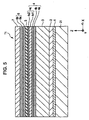
- Fig. 1 is a cross-sectional view of a tunnel magnetoresistive sensor (tunnel magnetoresistance effect device) according to the present embodiment, taken parallel to a plane of a recording medium.
- a tunnel magnetoresistive sensor is installed on a trailing edge of a flying slider in a hard disk drive and detects a recording magnetic field of a hard disk.
- a tunnel magnetoresistive sensor is also used in a magnetoresistive random access memory (MRAM).
- MRAM magnetoresistive random access memory
- the X direction is a track width direction.
- the Y direction is a direction of a leakage field from a magnetic recording medium (height direction).
- the Z direction is a direction of movement of a magnetic recording medium such as a hard disk and a lamination direction of the tunnel magnetoresistive sensor.
- the bottom layer in Fig. 1 is a first shielding layer 21, for example, formed of a NiFe alloy.
- the layered body T1 is formed on the first shielding layer 21.
- the tunnel magnetoresistive sensor is composed of the layered body T1, first insulating layers 22 formed on both sides of the layered body T1 in the track width direction (X direction in Fig. 1 ), hard bias layers 23, and second insulating layers 24.
- the bottom layer of the layered body T1 is an underlying layer 1 formed of a nonmagnetic material composed of at least one element selected from the group consisting of Ta, Hf, Nb, Zr, Ti, Mo, and W.
- a seed layer 2 is formed on the underlying layer 1.
- the seed layer 2. may be formed of Ru or NiFeCr.
- the seed layer 2 formed of NiFeCr has equivalent crystal faces of a face-centered cubic (fcc) structure represented by a ⁇ 111 ⁇ plane preferentially oriented parallel to the seed layer 2.
- the seed layer 2 formed of Ru has equivalent crystal faces of a hexagonal closest packed (hcp) structure represented by a ⁇ 000 ⁇ plane preferentially oriented parallel to the seed layer 2.
- the underlying layer 1 may be eliminated.
- An antiferromagnetic layer 3 formed on the seed layer 2 is preferably formed of an antiferromagnetic material containing an element ⁇ (wherein ⁇ is one or at least two elements selected from the group consisting of Pt, Pd, Ir, Rh, Ru, and Os) and Mn.
- ⁇ -Mn alloys containing an element of the platinum group have excellent characteristics as antiferromagnetic materials, such as high corrosion resistance and high blocking temperature. Furthermore, the ⁇ -Mn alloys can have an increased exchange coupling magnetic field (Hex).
- the antiferromagnetic layer 3 may be formed of an antiferromagnetic material containing an element ⁇ , an element ⁇ ' (wherein the element ⁇ ' is at least one element selected from the group consisting of Ne, Ar, Kr, Xe, Be, B, C, N, Mg, Al, Si, P, Ti, V, Cr, Fe, Co, Ni, Cu, Zn, Ga, Ge, Zr, Nb, Mo, Ag, Cd, Sn, Hf, Ta, W, Re, Au, Pb, and rare earth elements), and Mn.
- the element ⁇ ' is at least one element selected from the group consisting of Ne, Ar, Kr, Xe, Be, B, C, N, Mg, Al, Si, P, Ti, V, Cr, Fe, Co, Ni, Cu, Zn, Ga, Ge, Zr, Nb, Mo, Ag, Cd, Sn, Hf, Ta, W, Re, Au, Pb, and rare earth elements
- a pinned magnetic layer 4 is formed on the antiferromagnetic layer 3.
- the pinned magnetic layer 4 has a layered ferri structure including a first pinned magnetic sublayer 4a, a nonmagnetic intermediate sublayer 4b, and a second pinned magnetic sublayer (barrier-layer-side magnetic sublayer) 4c laminated in that order from the bottom.
- the directions of magnetization of the first pinned magnetic sublayer 4a and the second pinned magnetic sublayer 4c are brought into an antiparallel state by an exchange coupling magnetic field at an interface between the antiferromagnetic layer 3 and the pinned magnetic layer 4 and an antiferromagnetic exchange coupling magnetic field via the nonmagnetic intermediate sublayer 4b (RKKY interaction). This is a so-called layered ferri structure.
- the first pinned magnetic sublayer 4a has a thickness in the range of 1.2 to 3.2 nm (12 to 32 angstroms)
- the nonmagnetic intermediate sublayer 4b has a thickness approximately in the range of 0.8 to 1 nm (8 to 10 angstroms)
- the second pinned magnetic sublayer 4c has a thickness in the range of 1.6 to 4.2 nm (16 to 42 angstaoms).
- the first pinned magnetic sublayer 4a is formed of a ferromagnetic material such as CoFe, NiFe, or CoFeNi.
- the nonmagnetic intermediate sublayer 4b is formed of a nonmagnetic conductive material such as Ru, Rh, Ir, Cr, Re, or Cu.
- the second pinned magnetic sublayer 4c is composed of a first magnetic subsublayer 4cl formed of CoFeB or FeB and a second magnetic subsublayer 4c2 formed of CoFe or Fe.
- An insulating barrier layer 5 formed on the pinned magnetic layer 4 is formed of magnesium oxide (Mg-O).
- the insulating barrier layer 5 has a thickness approximately in the range of 0.6 to 1.2 nm.
- Mg-O preferably contains 40 to 60 atomic percent of Mg and is most preferably Mg 50at% O 50at% .
- a Mg layer having a very small thickness may be formed between the insulating barrier layer 5 and the second pinned magnetic sublayer 4c.
- a free magnetic layer 6 is formed on the insulating barrier layer 5.
- the free magnetic layer 6 is composed of a soft magnetic sublayer 6b formed of a magnetic material such as a NiFe alloy and an enhance sublayer 6a formed of a CoFe alloy.
- the enhance sublayer 6a is disposed between the soft magnetic sublayer 6b and the insulating barrier layer 5.
- the soft magnetic sublayer 6b is formed of a magnetic material having excellent soft magnetism.
- the enhance sublayer 6a is formed of a magnetic material having spin polarizability larger than that of the soft magnetic sublayer 6b.
- the enhance sublayer 6a formed of a CoFe alloy having large spin polarizability can improve the rate of resistance change ( ⁇ R/R).
- the free magnetic layer 6 may be a layered ferri structure in which a plurality of magnetic sublayers is laminated with nonmagnetic intermediate sublayers.
- the width of the free magnetic layer 6 in the track width direction (X direction in Fig. 1 ) defines the track width Tw.
- a protective layer 7, for example, formed of Ta is formed on the free magnetic layer 6.
- End faces 12 on both sides of the layered body T1 in the track width direction have inclined faces formed such that the width of the layered body T1 in the track width direction decreases gradually from the bottom to the top.
- the first insulating layers 22 disposed on both sides of the layered body T1 are formed on the first shielding layer 21 along the end faces 12 of the layered body T1.
- the hard bias layers 23 are formed on the first insulating layers 22.
- the second insulating layers 24 are formed on the hard bias layers 23.
- Bias underlying layers may be formed between the first insulating layers 22 and the hard bias layers 23.
- the bias underlying layers may be formed of Cr, W, and/or Ti.
- the first insulating layers 22 and the second insulating layers 24 are formed of an insulating material such as Al 2 O 3 or SiO 2 .
- the first insulating layers 22 and the second insulating layers 24 insulate the hard bias layers 23 to prevent an electric current flowing through the layered body T1 in a direction perpendicular to the interfaces of the layers of the layered body T1 from being shunted to both sides of the layered body T1 in the track width direction.
- the hard bias layers 23 are formed of a Co-Pt (cobalt-platinum) alloy or a Co-Cr-Pt (cobalt-chromium-platinum) alloy.
- a second shielding layer 26, for example, formed of a NiFe alloy is formed on the layered body T1 and the second insulating layers 24.
- the first shielding layer 21 and the second shielding layer 26 function as electrode layers of the layered body T1.
- an electric current flows in a direction perpendicular to the layers of the layered body T1 (in a direction parallel to the Z direction in Fig. 1 ).
- the free magnetic layer 6 is magnetized in a direction parallel to the track width direction (X direction in Fig. 1 ) under the influence of a bias magnetic field of the hard bias layers 23.
- the first pinned magnetic sublayer 4a and the second pinned magnetic sublayer 4c together constituting the pinned magnetic layer 4 are magnetized in a direction parallel to the height direction (Y direction in Fig. 1 ). Because the pinned magnetic layer 4 has a layered ferri structure, the magnetization of the first pinned magnetic sublayer 4a is antiparallel to the magnetization of the second pinned magnetic sublayer 4c. While the magnetization of the pinned magnetic layer 4 is fixed (an external magnetic field does not change the magnetization), the magnetization of the free magnetic layer 6 changes with the external magnetic field.
- an external magnetic field changes the magnetization of the free magnetic layer 6 and thereby changes the electrical resistance.
- the tunnel magnetoresistive sensor detects the change in electrical resistance as a voltage change and thereby detects a leakage field from a recording medium.
- the insulating barrier layer 5 is formed of magnesium oxide (Mg-O).
- the second pinned magnetic sublayer 4c constituting the pinned magnetic layer 4 underlying the insulating barrier layer 5 is formed in contact with the insulating barrier layer 5.
- the second pinned magnetic sublayer 4c is composed of the first magnetic subsublayer 4cl formed of CoFeB or FeB and the second magnetic subsublayer 4c2 formed of CoFe or Fe.
- the second magnetic subsublayer 4c2 is disposed between the first magnetic subsublayer 4c1 and the insulating barrier layer 5.
- this structure can achieve a higher rate of resistance change ( ⁇ R/R) than a conventional example in which the second pinned magnetic sublayer 4c is formed of a CoFeB monolayer.
- a tunnel magnetoresistive sensor can have a high head output even at a narrower track.
- the first magnetic subsublayer 4c1 formed of CoFeB or FeB having a tendency of becoming amorphous when the first magnetic subsublayer 4c1 formed of CoFeB or FeB having a tendency of becoming amorphous is formed on the nonmagnetic intermediate sublayer 4b in a non-heat-treated (as deposited) state, the first magnetic subsublayer 4c1 may block the influence of the crystalline orientation exerted by the crystal structures of from the seed layer 2 to the nonmagnetic intermediate sublayer 4b (for example, the orientation of a face-centered cubic structure ⁇ 111 ⁇ plane).
- the crystal structures of the second magnetic subsublayer 4c2, the insulating barrier layer 5, and the free magnetic layer 6 formed on the first magnetic subsublayer 4c1 may be less affected by the crystalline orientation of the crystal structures of from the seed layer 2 to the nonmagnetic intermediate sublayer 4b.
- the second magnetic subsublayer 4c2 formed of CoFe or Fe which is easy to crystallize, is formed on the first magnetic subsublayer 4c1
- preferred orientation of equivalent crystal faces of a body-centered cubic (bcc) structure represented by a ⁇ 100 ⁇ plane tends to occur in the second pinned magnetic sublayer 4c, the insulating barrier layer 5, and the enhance sublayer 6a formed of CoFe after heat treatment.
- crystal faces represented by a ⁇ 100 ⁇ plane refers to crystal faces expressed by Miller indices.
- the equivalent crystal faces represented by a ⁇ 100 ⁇ plane include a (100) plane, a (-100) plane, a (010) plane a (0-10) plane, a (001) plane, and a (00-1) plane.
- the present embodiment can achieve a higher rate of resistance change ( ⁇ R/R) than before.
- the thickness of the first magnetic subsublayer 4c1 is preferably in the range of 10 to 30 angstroms and is more preferably in the range of 16 to 24 angstroms. According to an experiment described below, a change in the thickness of the first magnetic subsublayer 4c1 does not cause a large change in the rate of resistance change ( ⁇ R/R). However, because an increased thickness of the first magnetic subsublayer 4c1 results in an increase in the B content in the entire second pinned magnetic sublayer 4c, it will have an influence on the crystallization of the second magnetic subsublayer 4c2 formed on the first magnetic subsublayer 4c1. Hence, the thickness of the first magnetic subsublayer 4c1 is preferably in the range described above.
- the thickness of the second magnetic subsublayer 4c2 is preferably in the range of 6 to 12 angstroms and is more preferably in the range of 7 to 11 angstroms. According to an experiment described below, when the thickness of the second magnetic subsublayer is smaller than 6 angstroms or larger than 12 angstroms, the rate of resistance change ( ⁇ R/R) is not increased. In contrast, when the thickness of a second magnetic subsublayer 4c2 is in the range of 7 to 11 angstroms, a high rate of resistance change ( ⁇ R/R) is achieved consistently. According to another experiment described below, the thickness of the second magnetic subsublayer 4c2 in the range described above can reduce the interlayer coupling magnetic field (Hin) between the free magnetic layer 6 and the pinned magnetic layer 4. Furthermore, in terms of the interlayer coupling magnetic field (Hin), the thickness of the second magnetic subsublayer 4c2 is preferably as large as possible within the range described above.
- the first magnetic subsublayer 4c1 is preferably formed of (Co X Fe 100-X ) 100-Y B Y , wherein the composition ratio Y of B is in the range of 15 to 30 atomic percent.
- the composition of the first magnetic subsublayer 4c1 can be controlled within the range described above to achieve a high rate of resistance change ( ⁇ R/R).
- the atomic ratio X ⁇ composition ratio of Co/(composition ratio of Co + composition ratio of Fe) ⁇ is preferably in the range of 0% to 80%.
- the second magnetic subsublayer 4c2 is preferably formed of Co Z Fe 100-Z , wherein the composition ratio Z of Co is in the range of 0 to 80 atomic percent. More preferably, the composition ratio Z of Co is in the range of 10 to 50 atomic percent.
- a tunnel magnetoresistive sensor is subjected to annealing (heat treatment) in a manufacturing process.
- annealing is performed at a temperature approximately in the range of 200°C to 310°C.
- Annealing may be performed in a magnetic field to generate an exchange coupling magnetic field (Hex) between the first pinned magnetic sublayer 4a constituting the pinned magnetic layer 4 and the antiferromagnetic layer 3.
- Hex exchange coupling magnetic field
- the annealing temperature when the annealing temperature is lower than 200°C, no interdiffusion of a component element may occur at an interface between the second magnetic subsublayer 4c2 and the first magnetic subsublayer 4c1, or, if any, the interdiffusion of a component element may occur on a small scale (for example, the interdiffusion does not occur over the entire interface but occurs intermittently). Thus, the state of the interface may be almost maintained.
- the interdiffusion of a component element may occur at an interface between the second magnetic subsublayer 4c2 and the first magnetic subsublayer 4c1, as illustrated in Fig. 2 or 3 .
- the interdiffusion of a component element can eliminate the interface and form a composition modulation region with respect to the concentration of B.
- element diffusion occurs at an interface between the second magnetic subsublayer 4c2 and the first magnetic subsublayer 4c1.
- the second pinned magnetic sublayer 4c is composed of a first magnetic region 10 formed of CoFeB or FeB and a second magnetic region 11 formed of CoFe or Fe.
- the second magnetic region 11 is disposed between the first magnetic region 10 and the insulating barrier layer 5.
- the second magnetic region 11 is free of B.
- the first magnetic region 10 includes a composition modulation region in which the concentration of B decreases gradually from an undersurface (interface in contact with the nonmagnetic intermediate sublayer 4b) toward the second magnetic region 11.
- the concentration of B in the vicinity of the undersurface of the first magnetic region 10 is lower than that in the inside of the first magnetic region 10. This results from element diffusion between the first magnetic region 10 and the nonmagnetic intermediate sublayer 4b.
- the second pinned magnetic sublayer 4c is entirely formed of CoFeB.
- the concentration of B is lower in the top surface side in contact with the insulating barrier layer 5 than in the undersurface side in contact with the nonmagnetic intermediate sublayer 4b.
- the second pinned magnetic sublayer 4c includes a composition modulation region in which the concentration of B decreases gradually from the undersurface side in contact with the nonmagnetic intermediate sublayer 4b to the top surface side in contact with the insulating barrier layer 5.
- the concentration of B in the vicinity of the undersurface of the second pinned magnetic sublayer 4c is lower than that in the inside of the second pinned magnetic sublayer 4c. This results from element diffusion between the second pinned magnetic sublayer 4c and the nonmagnetic intermediate sublayer 4b.
- the pinned magnetic layer 4 has a layered ferri structure composed of the first pinned magnetic sublayer 4a, the nonmagnetic intermediate sublayer 4b, and the second pinned magnetic sublayer 4c.
- the present embodiment can be applied to the pinned magnetic layer 4 having a monolayer structure or a layered structure composed of a plurality of magnetic layers.
- the magnetization of the pinned magnetic layer 4 can be fixed more appropriately.
- the pinned magnetic layer 4 having a layered ferri structure is therefore suitable to improve the playback output.
- the embodiment illustrated in Fig. 1 is a so-called bottom-type tunnel magnetoresistive sensor, in which the insulating barrier layer 5 is formed on the pinned magnetic layer 4.
- the present embodiment can also be applied to a so-called top-type layered structure, in which the pinned magnetic layer 4 is formed on the insulating barrier layer 5.
- the free magnetic layer 6, the insulating barrier layer 5, the pinned magnetic layer 4, and the antiferromagnetic layer 3 are laminated in that order from the bottom.
- the second pinned magnetic sublayer 4c constituting the pinned magnetic layer 4 is composed of the second magnetic subsublayer 4c2 formed of CoFe or Fe and the first magnetic subsublayer 4c1 formed of CoFeB or FeB laminated in that order from the bottom. Element diffusion may occur between the second magnetic subsublayer 4c2 and the first magnetic subsublayer 4cl.
- the present embodiment can also be applied to a dual-type tunnel magnetoresistive sensor composed of a first antiferromagnetic layer, a first pinned magnetic layer, a first insulating barrier layer, a free magnetic layer, a second insulating barrier layer, a second pinned magnetic layer, and a second antiferromagnetic layer laminated in that order from the bottom.
- the structure of the first pinned magnetic layer is described in Figs. 1 to 3 .
- the structure of the second pinned magnetic layer is described for the top-type layered structure.
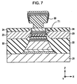
- FIGs. 4 to 7 are fragmentary sectional views of a tunnel magnetoresistive sensor in a manufacturing process, taken in the same direction as in Fig. 1 .
- an underlying layer 1 a seed layer 2, an antiferromagnetic layer 3, a first pinned magnetic sublayer 4a, a nonmagnetic intermediate sublayer 4b, and a second pinned magnetic sublayer 4c are successively formed on a first shielding layer 21.
- These layers may be deposited by sputtering.
- the second pinned magnetic sublayer 4c is composed of a first magnetic subsublayer 4c1 formed of CoFeB or FeB and a second magnetic subsublayer 4c2 formed of CoFe or Fe laminated in that order from the bottom.
- the first magnetic subsublayer 4c1 is preferably formed of (Co X Fe 100-X ) 100-Y B Y , wherein the composition ratio Y of B is in the range of 15 to 30 atomic percent, and the atomic ratio X is in the range of 0% to 80%. Furthermore, the first magnetic subsublayer 4c1 preferably has an average thickness in the range of 1 to 3 nm (10 to 30 angstroms). This can achieve a high rate of resistance change ( ⁇ R/R).
- the second magnetic subsublayer 4c2 is preferably formed of Co Z Fe 100-Z , wherein the composition ratio Z of Co is controlled within the range of 0 to 80 atomic percent. Furthermore, the second magnetic subsublayer 4c2 preferably has an average thickness in the range of 0.6 to 1.2 nm (6 to 12 angstroms). This can achieve a high rate of resistance change ( ⁇ R/R).
- the surface of the second pinned magnetic sublayer 4c is then subjected to plasma processing.
- the plasma processing is performed to improve the flatness of the surface of the second pinned magnetic sublayer 4c.
- the surface of the second pinned magnetic sublayer 4c is also sufficiently flat. The plasma processing may therefore be eliminated.
- An insulating barrier layer 5 formed of Mg-O is then formed on the second pinned magnetic sublayer 4c.
- the insulating barrier layer 5 formed of Mg-O is directly formed, for example, by RF sputtering, using a Mg-O target.
- a Mg layer may be formed on the second pinned magnetic sublayer 4c by sputtering, and the Mg layer may be oxidized to form the insulating barrier layer 5 formed of Mg-O.
- the oxidizing method include radical oxidation, ion oxidation, plasma oxidation, and natural oxidation.
- the Mg layer has a thickness approximately in the range of 0.2 to 1 nm (2 to 10 angstroms).
- a free magnetic layer 6 composed of an enhance sublayer 6a and a soft magnetic sublayer 6b, and a protective layer 7 are formed on the insulating barrier layer 5.
- the enhance sublayer 6a is preferably formed of CoFe in which the Fe composition ratio is in the range of 5 to 90 atomic percent.
- the soft magnetic sublayer 6b is preferably formed of a NiFe alloy in which the Ni composition ratio is in the range of 78 to 92 atomic percent.
- a layered body T1 including from the underlying layer 1 to the protective layer 7 is formed.
- a lift-off resist layer 30 is then formed on the layered body T1. Both ends of the layered body T1 in the track width direction (X direction) that are not covered with the lift-off resist layer 30 are removed, for example, by etching (see Fig. 6 ).
- First insulating layers 22, hard bias layers 23, and second insulating layers 24 are then stacked on the first shielding layer 21 on both sides of the layered body T1 in the track width direction (X direction) in that order from the bottom (see Fig. 7 ).
- the lift-off resist layer 30 is then removed to form a second shielding layer 26 on the layered body T1 and the second insulating layers 24.
- the method for manufacturing a tunnel magnetoresistive sensor described above includes annealing. Annealing is typically performed to generate an exchange coupling magnetic field (Hex) between the antiferromagnetic layer 3 and the first pinned magnetic sublayer 4a.
- Hex exchange coupling magnetic field
- the annealing temperature is lower than 200°C, no interdiffusion of a component element may occur at interfaces between the layers, or, if any, the interdiffusion of a component element may occur on a small scale (for example, the interdiffusion does not occur over the entire interface but occurs intermittently). Thus, the state of the interface may be almost maintained.
- the interdiffusion of a component element may occur at interfaces between the layers.
- the interdiffusion of a component element can eliminate an interface between the first magnetic subsublayer 4c1 and the second magnetic subsublayer 4c2 in the second pinned magnetic sublayer 4c and form a composition modulation region with respect to the concentration of B.
- a tunnel magnetoresistive sensor that can achieve a high rate of resistance change ( ⁇ R/R) can easily and appropriately be manufactured by the manufacturing methods described above.
- the two-layered structure of the second pinned magnetic sublayer 4c composed of the first magnetic subsublayer 4c1 and the second magnetic subsublayer 4c2 as described above can achieve a higher rate of resistance change ( ⁇ R/R) than a conventional example in which the second pinned magnetic sublayer 4c is formed of a CoFeB monolayer.
- the manufacturing method according to the present embodiment is a method for manufacturing a so-called bottom-type tunnel magnetoresistive sensor.
- the manufacturing method can be applied to so-called top-type tunnel magnetoresistive sensors or dual-type tunnel magnetoresistive sensors.
- a tunnel magnetoresistive sensor illustrated in Fig. 1 was formed.
- a layered body T1 was composed of an underlying layer 1; Ta (30)/seed layer 2; Ru (40)/antiferromagnetic layer 3; IrMn (70)/pinned magnetic layer 4 [first pinned magnetic sublayer 4a; Co 70at% Fe 30at% (22)/nonmagnetic intermediate sublayer 4b; Ru (9.
- the surface of the second pinned magnetic sublayer 4c was subjected to plasma processing before the formation of the insulating barrier layer 5.
- the insulating barrier layer 5 was then formed on the second pinned magnetic sublayer 4c by sputtering using a Mg-O target.
- the layered body was annealed at 270°C for 3.5 hours.
- the following structures were formed as the second pinned magnetic sublayer 4c.
- a layered structure composed of (Co 50% Fe 50% ) 85at% B 15at% (22)/Co 50at% Fe 50at% (4) laminated in that order from the bottom.
- a layered structure composed of (Co 50% Fe 50% ) 77at% B 23at% (20)/Co 50at% Fe 50at% (6) laminated in that order from the bottom.
- a layered structure composed of (Co 50% Fe 50% ) 70at% B 30at% (18)/Co 50at% Fe 50at% (8) laminated in that order from the bottom.
- a layered structure composed of (Co 50% Fe 50% ) 70at% B 30at% (t1)/Co 50at% Fe 50at% (8) laminated in that order from the bottom, wherein the thickness t1 of a first magnetic subsublayer 4c1 is 1.6, 1.8, 2, 2.2 or 2.4 nm (16, 18, 20, 22, or 24 angstroms).
- a layered structure composed of (Co 50% Fe 50% ) 70at% B 30at% (t1)/Co 50at% Fe 50at% (9) laminated in that order from the bottom, wherein the thickness t1 of a first magnetic subsublayer 4c1 is 1.6, 1.8, 2, 2.2 or 2.4 nm (16, 18, 20, 22, or 24 angstroms).
- a layered structure composed of (Co 50% Fe 50% ) 70at% B 30at% (t1)/Co 50at% Fe 50at% (10) laminated in that order from the bottom, wherein the thickness t1 of a first magnetic subsublayer 4c1 is 1.6, 1.8, 2, 2.2 or 2.4 nm (16, 18, 20, 22, or 24 angstroms).
- a layered structure composed of (Co 50% Fe 50% ) 70at% B 30at% (20)/Co 50at% Fe 50at% (t2) laminated in that order from the bottom, wherein the thickness t2 of a second magnetic subsublayer 4c2 is 0.6, 0.7, 0.8, 0.9, 1, 1.1 or 1.2 nm (6, 7, 8, 9, 10, 11, or 12 angstroms).
- the rate of resistance change ( ⁇ R/R), RA (resistance R x area A), and the interlayer coupling magnetic field (Hin) were determined.
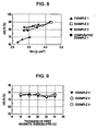
- Fig. 8 shows the relationship between RA and the rate of resistance change ( ⁇ R/R) in Examples 1 to 3 and Comparative Example 1.
- RA of each sample of Examples 1 to 3 and Comparative Example 1 was changed by changing the thickness of the insulating barrier layer 5 formed of Mg-O within the range of 0.8 to 1.2 nm (8 to 12 angstroms).
- Examples 1 to 3 in which the second pinned magnetic sublayer 4c was a layered structure composed of the first magnetic subsublayer 4c1 and the second magnetic subsublayer 4c2, had a higher rate of resistance change ( ⁇ R/R) than Comparative Example 1, in which the second pinned magnetic sublayer 4c was formed only of the first magnetic subsublayer. Furthermore, while Examples 1 to 3 had a little larger RAs than Comparative Example 1, it does not have a large effect on the characteristics of a head.
- Fig. 9 shows the relationship between the thickness (t1) of a first magnetic subsublayer 4c1 and the rate of resistance change ( ⁇ R/R) in Examples 4 to 6.
- Fig. 9 shows that, when the thickness of a first magnetic subsublayer 4c1 formed of CoFeB was in the range of 1.6 to 2.4 nm (16 to 24 angstroms), the rate of resistance change ( ⁇ R/R) was almost constant.
- Fig. 10 shows the rate of resistance change ( ⁇ R/R) in Examples 7 to 13, in which the thickness (t2) of the second magnetic subsublayer 4c2 was in the range of 0.6 to 1.2 nm (6 to 12 angstroms), and Comparative Example 1, in which the second pinned magnetic sublayer 4c was formed of a CoFeB monolayer (that is, the thickness of the second magnetic subsublayer 4c2 was zero angstroms).
- Fig. 10 shows that Examples 7 to 13, in which the thickness of the second magnetic subsublayer 4c2 was in the range of 0.6 to 1.2 nm (6 to 12 angstroms), had a higher rate of resistance change ( ⁇ R/R) than Comparative Example 1, in which the thickness of the second magnetic subsublayer 4c2 was zero angstroms. Furthermore, it was found that when the thickness of the second magnetic subsublayer 4c2 was in the range of 0.7 to 1.1 nm (7 to 11 angstroms), in particular in the range of 0.8 to 1 nm (8 to 10 angstroms), a much higher rate of resistance change ( ⁇ R/R) was achieved.
- Fig. 11 shows the interlayer coupling magnetic field (Hin) between the free magnetic layer 6 and the pinned magnetic layer 4 in Examples 7 to 13 and Comparative Example 1.
- Fig. 11 shows that when the thickness of the second magnetic subsublayer 4c2 was in the range of 0.6 to 1.2 nm (6 to 12 angstroms), the interlayer coupling magnetic field Hin could be larger than that of Comparative Example 1. Thus, it is believed that the flatness of an interface between the pinned magnetic layer and the insulating barrier layer was improved in the present examples relative to Comparative Example 1. Furthermore, as shown in Fig. 11 , in the examples, the interlayer coupling magnetic field Hin was found to decrease with increasing average thickness of the second magnetic subsublayer (CoFe layer). Thus, when the average thickness of the second magnetic subsublayer 4c2 is in the range of 0.6 to 1.2 nm (6 to 12 angstroms), a larger average thickness within this range will be preferred.
Landscapes
- Engineering & Computer Science (AREA)
- Chemical & Material Sciences (AREA)
- Nanotechnology (AREA)
- Physics & Mathematics (AREA)
- Crystallography & Structural Chemistry (AREA)
- Manufacturing & Machinery (AREA)
- Condensed Matter Physics & Semiconductors (AREA)
- Power Engineering (AREA)
- General Physics & Mathematics (AREA)
- Spectroscopy & Molecular Physics (AREA)
- Computer Hardware Design (AREA)
- Mathematical Physics (AREA)
- Theoretical Computer Science (AREA)
- Hall/Mr Elements (AREA)
- Measuring Magnetic Variables (AREA)
- Mram Or Spin Memory Techniques (AREA)
- Magnetic Heads (AREA)
- Thin Magnetic Films (AREA)
Claims (20)
- Capteur magnétorésistif à effet tunnel, dans lequel :une couche magnétique fixe (4) ayant une magnétisation fixe, une couche formant barrière isolante (5), et une couche magnétique libre (6) ayant une magnétisation variable en fonction d'un champ magnétique extérieur sont superposées dans cet ordre en partant du bas, ou la couche magnétique libre, la couche formant barrière isolante et la couche magnétique fixe sont superposées dans cet ordre en partant du bas,la couche formant barrière isolante est faite de Mg-O, etune sous-couche magnétique côté couche de barrière (4c) constituant au moins une partie de la couche magnétique fixe et étant en contact avec la couche formant barrière isolante comprend une première région magnétique (4c1) en CoFeB ou FeB et une deuxième région magnétique (4c2) en CoFe ou Fe, la deuxième région magnétique étant placée entre la première région magnétique et la couche formant barrière isolante.
- Capteur magnétorésistif à effet tunnel selon la revendication 1, dans lequel la première région magnétique comprend une région de modulation de composition dans laquelle la concentration de B diminue progressivement d'une première limite de la première région magnétique vers la deuxième région magnétique, la première limite étant opposée à une deuxième limite entre la première région magnétique et la deuxième région magnétique.
- Capteur magnétorésistif à effet tunnel selon la revendication 1 ou 2, dans lequel la sous-couche magnétique côté couche de barrière est formée par diffusion d'éléments au niveau d'une interface entre une première sous sous-couche magnétique en CoFeB ou FeB et une deuxième sous sous-couche magnétique en CoFe ou Fe, la deuxième sous sous-couche magnétique étant placée entre la première sous sous-couche magnétique et la couche formant barrière isolante, dans une structure stratifiée comprenant la première sous sous-couche magnétique et la deuxième sous sous-couche magnétique.
- Capteur magnétorésistif à effet tunnel dans lequel :une couche magnétique fixe (4) ayant une magnétisation fixe, une couche formant barrière isolante (5), et une couche magnétique libre (6) ayant une magnétisation variable en fonction d'un champ magnétique extérieur sont superposées dans cet ordre en partant du bas, ou la couche magnétique libre, la couche formant barrière isolante et la couche magnétique fixe sont superposées dans cet ordre en partant du bas,la couche formant barrière isolante est faite de Mg-O, etune sous-couche magnétique côté couche de barrière (4c) constituant au moins une partie de la couche magnétique fixe et étant en contact avec la couche formant barrière isolante a une structure stratifiée comprenant une première sous sous-couche magnétique (4c1) en CoFeB ou FeB et une deuxième sous sous-couche magnétique (4c2) en CoFe ou Fe, la deuxième sous sous-couche magnétique étant placée entre la première sous sous-couche magnétique et la couche formant barrière isolante.
- Capteur magnétorésistif à effet tunnel selon la revendication 3 ou 4, dans lequel la première sous sous-couche magnétique est en (CoxFe100-x)100-yBy, dans lequel le taux de composition Y de B est compris dans l'intervalle de 15 à 30 pour cent atomique.
- Capteur magnétorésistif à effet tunnel selon l'une quelconque des revendications 3 à 5, dans lequel l'épaisseur moyenne de la première sous sous-couche magnétique vaut de 1 à 3 nm (10 à 30 angströms).
- Capteur magnétorésistif à effet tunnel selon l'une quelconque des revendications 3 à 6, dans lequel la deuxième sous sous-couche magnétique est en CozFe100-z, dans lequel le taux de composition z de Co est compris dans l'intervalle de 0 à 80 pour cent atomique.
- Capteur magnétorésistif à effet tunnel selon l'une quelconque des revendications 3 à 7, dans lequel l'épaisseur moyenne de la deuxième sous sous-couche magnétique vaut de 0,6 à 1,2 nm (6 à 12 angströms).
- Capteur magnétorésistif à effet tunnel selon l'une quelconque des revendications 1 à 8, dans lequel la sous-couche magnétique côté couche de barrière, la couche formant barrière isolante et au moins une partie de la couche magnétique libre en contact avec la couche formant barrière isolante ont des faces de cristal équivalentes d'une structure cubique à corps centré représentée par un plan {100} orienté de préférence parallèlement aux couches.
- Capteur magnétorésistif à effet tunnel selon l'une quelconque des revendications 1 à 9, dans lequel la couche magnétique fixe a une structure ferrimagnétique stratifiée comprenant une première sous-couche magnétique fixe, une sous-couche intermédiaire non magnétique et une deuxième sous-couche magnétique fixe superposées dans cet ordre, la deuxième sous-couche magnétique fixe étant la sous-couche magnétique côté couche de barrière en contact avec la couche formant barrière isolante.
- Capteur magnétorésistif à effet tunnel selon l'une quelconque des revendications 1 à 10, dans lequel la couche magnétique libre comprend une sous-couche à enrichissement et une sous-couche faiblement ferromagnétique placée sur la sous-couche à enrichissement, la sous-couche à enrichissement étant en contact avec la couche formant barrière isolante et étant faite de CoFe, la sous-couche faiblement ferromagnétique étant faite d'un alliage NiFe.
- Procédé de fabrication d'un capteur magnétorésistif à effet tunnel comprenant une partie stratifiée, la partie stratifiée comprenant une couche magnétique fixe (4) ayant une direction de magnétisation fixe, une couche formant barrière isolante (5), et une couche magnétique libre (6) ayant une direction de magnétisation variable en fonction d'un champ magnétique extérieur superposées dans cet ordre en partant du bas, le procédé comprenant les étapes suivantes :(a) empiler une deuxième sous sous-couche magnétique en CoFe ou Fe sur une première sous sous-couche magnétique en CoFeB ou FeB pour former une sous-couche magnétique côté couche de barrière constituant au moins une partie de la couche magnétique fixe ;(b) former une couche formant barrière isolante faite de Mg-O sur la sous-couche magnétique côté couche de barrière ; et(c) former la couche magnétique libre sur la couche de barrière isolante.
- Procédé de fabrication d'un capteur magnétorésistif à effet tunnel comprenant une partie stratifiée, la partie stratifiée comprenant une couche magnétique libre (4) ayant une direction de magnétisation variable en fonction d'un champ magnétique extérieur, une couche formant barrière isolante (5), et une couche magnétique fixe (6) ayant une direction de magnétisation fixe superposées dans cet ordre en partant du bas, le procédé comprenant les étapes suivantes :(d) former la couche magnétique libre ;(e) former une couche formant barrière isolante faite de Mg-O sur la couche magnétique libre ; et(f) empiler une deuxième sous sous-couche magnétique en CoFe ou Fe et une première sous sous-couche magnétique en CoFeB ou FeB sur la couche formant barrière isolante pour former une sous-couche magnétique côté couche de barrière constituant au moins une partie de la couche magnétique fixe.
- Procédé de fabrication d'un capteur magnétorésistif à effet tunnel selon la revendication 12 ou 13, dans lequel, dans la formation de la première sous sous-couche magnétique, la première sous sous-couche magnétique est en (CoxFe100-x)100-yBy, dans lequel le taux de composition Y de B est ajusté dans l'intervalle de 15 à 30 pour cent atomique.
- Procédé de fabrication d'un capteur magnétorésistif à effet tunnel selon l'une quelconque des revendications 12 à 14, dans lequel la première sous sous-couche magnétique a une épaisseur moyenne de de 1 à 3 nm (10 à 30 angströms).
- Procédé de fabrication d'un capteur magnétorésistif à effet tunnel selon l'une quelconque des revendications 12 à 15, dans lequel, dans la formation de la deuxième sous sous-couche magnétique, la deuxième sous sous-couche magnétique est en CozFe100-z, dans lequel le taux de composition z de Co est ajusté dans l'intervalle de 0 à 80 pour cent atomique.
- Procédé de fabrication d'un capteur magnétorésistif à effet tunnel selon l'une quelconque des revendications 12 à 16, dans lequel la deuxième sous sous-couche magnétique a une épaisseur moyenne de 0,6 à 1,2 nm (6 à 12 angströms).
- Procédé de fabrication d'un capteur magnétorésistif à effet tunnel selon l'une quelconque des revendications 12 à 17, dans lequel, dans la formation de la couche formant barrière isolante, une couche de Mg est formée puis cette couche est oxydée pour former la couche formant barrière isolante en Mg-O.
- Procédé de fabrication d'un capteur magnétorésistif à effet tunnel selon l'une quelconque des revendications 12 à 18, dans lequel, dans la formation de la couche formant barrière isolante, la couche formant barrière isolante en Mg-O est formée en utilisant une cible en Mg-O.
- Procédé de fabrication d'un capteur magnétorésistif à effet tunnel selon l'une quelconque des revendications 12 à 19, dans lequel on exécute un recuit après la formation de la partie stratifiée.
Applications Claiming Priority (2)
| Application Number | Priority Date | Filing Date | Title |
|---|---|---|---|
| JP2006255646 | 2006-09-21 | ||
| JP2007065628A JP5210533B2 (ja) | 2006-09-21 | 2007-03-14 | トンネル型磁気検出素子及びその製造方法 |
Publications (3)
| Publication Number | Publication Date |
|---|---|
| EP1903624A2 EP1903624A2 (fr) | 2008-03-26 |
| EP1903624A3 EP1903624A3 (fr) | 2011-08-31 |
| EP1903624B1 true EP1903624B1 (fr) | 2012-07-25 |
Family
ID=38896956
Family Applications (1)
| Application Number | Title | Priority Date | Filing Date |
|---|---|---|---|
| EP07018080A Not-in-force EP1903624B1 (fr) | 2006-09-21 | 2007-09-14 | Détecteur magnéto-résistant à tunnel dans lequel au moins une partie de la couche d'ancrage est composée d'une couche CoFeB et procédé de fabrication du détecteur magnéto-résistant à tunnel |
Country Status (3)
| Country | Link |
|---|---|
| US (1) | US7969693B2 (fr) |
| EP (1) | EP1903624B1 (fr) |
| JP (1) | JP5210533B2 (fr) |
Families Citing this family (27)
| Publication number | Priority date | Publication date | Assignee | Title |
|---|---|---|---|---|
| JP2008066640A (ja) * | 2006-09-11 | 2008-03-21 | Alps Electric Co Ltd | トンネル型磁気検出素子およびその製造方法 |
| JP4923896B2 (ja) * | 2006-09-15 | 2012-04-25 | 富士通株式会社 | 交換結合膜及び磁気デバイス |
| JP2008135432A (ja) * | 2006-11-27 | 2008-06-12 | Tdk Corp | トンネル磁気抵抗効果素子及びその製造方法 |
| US7940494B2 (en) * | 2007-01-16 | 2011-05-10 | Tdk Corporation | Magnetic recording medium, magnetic recording and reproducing apparatus, and method for manufacturing magnetic recording medium |
| WO2008126136A1 (fr) * | 2007-03-20 | 2008-10-23 | Fujitsu Limited | Tête magnétique |
| US7999336B2 (en) | 2008-04-24 | 2011-08-16 | Seagate Technology Llc | ST-RAM magnetic element configurations to reduce switching current |
| JPWO2010026703A1 (ja) * | 2008-09-02 | 2012-01-26 | キヤノンアネルバ株式会社 | 磁気抵抗素子とその製造方法、該製造方法に用いる記憶媒体 |
| WO2010026667A1 (fr) | 2008-09-03 | 2010-03-11 | Canon Anelva Corporation | Couche de germe de promotion de la croissance du grain préférée ferromagnétique pour barrière tunnel au mgo amorphe ou microcristalline |
| JP2010062353A (ja) | 2008-09-04 | 2010-03-18 | Fujitsu Ltd | 磁気抵抗効果素子 |
| US7940551B2 (en) | 2008-09-29 | 2011-05-10 | Seagate Technology, Llc | STRAM with electronically reflective insulative spacer |
| US7826256B2 (en) | 2008-09-29 | 2010-11-02 | Seagate Technology Llc | STRAM with compensation element |
| WO2010044134A1 (fr) * | 2008-10-14 | 2010-04-22 | キヤノンアネルバ株式会社 | Procédé de production d'élément à effet de magnétorésistance et programme de production d'élément à effet de magnétorésistance |
| US20100148167A1 (en) * | 2008-12-12 | 2010-06-17 | Everspin Technologies, Inc. | Magnetic tunnel junction stack |
| KR101584747B1 (ko) | 2009-01-20 | 2016-01-13 | 삼성전자주식회사 | 자기 메모리 소자 |
| JP2013048124A (ja) * | 2009-11-20 | 2013-03-07 | Fuji Electric Co Ltd | 強磁性トンネル接合素子 |
| US8508221B2 (en) * | 2010-08-30 | 2013-08-13 | Everspin Technologies, Inc. | Two-axis magnetic field sensor having reduced compensation angle for zero offset |
| JP2012204591A (ja) * | 2011-03-25 | 2012-10-22 | Toshiba Corp | 膜形成方法および不揮発性記憶装置 |
| US8686484B2 (en) | 2011-06-10 | 2014-04-01 | Everspin Technologies, Inc. | Spin-torque magnetoresistive memory element and method of fabricating same |
| SG11201504875UA (en) | 2012-12-20 | 2015-07-30 | Canon Anelva Corp | Method for manufacturing magnetoresistance effect element |
| JP2014157649A (ja) * | 2013-02-18 | 2014-08-28 | Toshiba Corp | 磁気抵抗効果素子、磁気ヘッド、磁気ヘッドアセンブリ及び磁気記録再生装置 |
| US9385309B2 (en) | 2014-04-28 | 2016-07-05 | Qualcomm Incorporated | Smooth seed layers with uniform crystalline texture for high perpendicular magnetic anisotropy materials |
| US10483320B2 (en) | 2015-12-10 | 2019-11-19 | Everspin Technologies, Inc. | Magnetoresistive stack with seed region and method of manufacturing the same |
| EP4514109A3 (fr) | 2015-12-10 | 2025-04-30 | Everspin Technologies, Inc. | Empilement magnétorésistif, zone initiale associée et procédé de fabrication associé |
| US10361361B2 (en) * | 2016-04-08 | 2019-07-23 | International Business Machines Corporation | Thin reference layer for STT MRAM |
| EP3460811B1 (fr) * | 2017-09-20 | 2020-06-17 | IMEC vzw | Structure magnétique stratifiée pour dispositif à jonction tunnel magnétique |
| CN112635652B (zh) * | 2019-10-08 | 2023-05-26 | 上海磁宇信息科技有限公司 | 磁性随机存储器的磁性隧道结结构 |
| CN112652702B (zh) * | 2019-10-10 | 2023-12-22 | 上海磁宇信息科技有限公司 | 磁性随机存储器的磁性隧道结结构 |
Family Cites Families (19)
| Publication number | Priority date | Publication date | Assignee | Title |
|---|---|---|---|---|
| US6436526B1 (en) * | 1999-06-17 | 2002-08-20 | Matsushita Electric Industrial Co., Ltd. | Magneto-resistance effect element, magneto-resistance effect memory cell, MRAM and method for performing information write to or read from the magneto-resistance effect memory cell |
| JP2003124541A (ja) * | 2001-10-12 | 2003-04-25 | Nec Corp | 交換結合膜、磁気抵抗効果素子、磁気ヘッド及び磁気ランダムアクセスメモリ |
| JP2004355669A (ja) * | 2003-05-27 | 2004-12-16 | Hitachi Ltd | 磁気記録ヘッド及びその製造方法 |
| JP3824600B2 (ja) * | 2003-07-30 | 2006-09-20 | 株式会社東芝 | 磁気抵抗効果素子および磁気メモリ |
| US7098495B2 (en) * | 2004-07-26 | 2006-08-29 | Freescale Semiconducor, Inc. | Magnetic tunnel junction element structures and methods for fabricating the same |
| JP4568152B2 (ja) * | 2004-09-17 | 2010-10-27 | 株式会社東芝 | 磁気記録素子及びそれを用いた磁気記録装置 |
| JP2006093432A (ja) * | 2004-09-24 | 2006-04-06 | Sony Corp | 記憶素子及びメモリ |
| JP5095076B2 (ja) * | 2004-11-09 | 2012-12-12 | 株式会社東芝 | 磁気抵抗効果素子 |
| JP2006139886A (ja) * | 2004-11-15 | 2006-06-01 | Hitachi Global Storage Technologies Netherlands Bv | 磁気抵抗効果型磁気ヘッド及びその製造方法 |
| JP4951858B2 (ja) * | 2005-01-12 | 2012-06-13 | ソニー株式会社 | メモリ |
| US20060171197A1 (en) * | 2005-01-31 | 2006-08-03 | Ulrich Klostermann | Magnetoresistive memory element having a stacked structure |
| JP2005197764A (ja) | 2005-03-22 | 2005-07-21 | Nec Corp | 磁気抵抗効果センサ、磁気抵抗検出システム、および磁気記憶システム |
| US7205596B2 (en) * | 2005-04-29 | 2007-04-17 | Infineon Technologies, Ag | Adiabatic rotational switching memory element including a ferromagnetic decoupling layer |
| US7800868B2 (en) * | 2005-12-16 | 2010-09-21 | Seagate Technology Llc | Magnetic sensing device including a sense enhancing layer |
| US7821747B2 (en) * | 2006-02-10 | 2010-10-26 | Hitachi Global Storage Technologies Netherlands B.V. | Method and apparatus for providing improved pinning structure for tunneling magnetoresistive sensor |
| US7672088B2 (en) * | 2006-06-21 | 2010-03-02 | Headway Technologies, Inc. | Heusler alloy with insertion layer to reduce the ordering temperature for CPP, TMR, MRAM, and other spintronics applications |
| US7760474B1 (en) * | 2006-07-14 | 2010-07-20 | Grandis, Inc. | Magnetic element utilizing free layer engineering |
| US7751156B2 (en) * | 2006-09-29 | 2010-07-06 | Hitachi Global Storage Technologies Netherlands, B.V. | Dual-layer free layer in a tunneling magnetoresistance (TMR) element |
| US7764468B2 (en) * | 2007-04-16 | 2010-07-27 | Tdk Corporation | Method for removing smear and magnetic recording/reproducing apparatus with function of removing smear |
-
2007
- 2007-03-14 JP JP2007065628A patent/JP5210533B2/ja not_active Expired - Fee Related
- 2007-09-14 EP EP07018080A patent/EP1903624B1/fr not_active Not-in-force
- 2007-09-19 US US11/857,921 patent/US7969693B2/en active Active
Also Published As
| Publication number | Publication date |
|---|---|
| JP2008103661A (ja) | 2008-05-01 |
| JP5210533B2 (ja) | 2013-06-12 |
| EP1903624A3 (fr) | 2011-08-31 |
| EP1903624A2 (fr) | 2008-03-26 |
| US7969693B2 (en) | 2011-06-28 |
| US20080074805A1 (en) | 2008-03-27 |
Similar Documents
| Publication | Publication Date | Title |
|---|---|---|
| EP1903624B1 (fr) | Détecteur magnéto-résistant à tunnel dans lequel au moins une partie de la couche d'ancrage est composée d'une couche CoFeB et procédé de fabrication du détecteur magnéto-résistant à tunnel | |
| JP4786331B2 (ja) | 磁気抵抗効果素子の製造方法 | |
| US8169752B2 (en) | Method for manufacturing a magneto-resistance effect element having spacer layer | |
| CN100557840C (zh) | CoFeB层构成固定层至少一部分的隧道型磁检测元件及其制法 | |
| US9028909B2 (en) | Magnetoresistive element and method of manufacturing the same | |
| US20080174921A1 (en) | TUNNEL TYPE MAGNETIC SENSOR HAVING FIXED MAGNETIC LAYER OF COMPOSITE STRUCTURE CONTAINING CoFeB FILM, AND METHOD FOR MANUFACTURING THE SAME | |
| US8009391B2 (en) | Magnetic sensing element and method for manufacturing the same | |
| US7898776B2 (en) | Tunneling magnetic sensing element including enhancing layer having high Fe concentration in the vicinity of barrier layer | |
| US8671554B2 (en) | Method of manufacturing a magneto-resistance effect element | |
| US20080186639A1 (en) | Tunneling magnetic sensing element and method for producing same | |
| US7787221B2 (en) | Tunneling magnetic sensing element including non-magnetic metal layer between magnetic layers | |
| US8045300B2 (en) | Tunneling magnetic sensing element and method for producing same | |
| US7643254B2 (en) | Tunnel-effect type magnetic sensor having free layer including non-magnetic metal layer | |
| US20080186638A1 (en) | Tunneling magnetic sensing element having free magnetic layer inserted with nonmagnetic metal layers | |
| JP2007194327A (ja) | トンネル型磁気検出素子 | |
| JP2007194457A (ja) | トンネル型磁気検出素子及びその製造方法 | |
| US7907370B2 (en) | Tunneling magnetic sensing element having free layer containing CoFe alloy | |
| US8124253B2 (en) | Tunneling magnetic sensing element including MGO film as insulating barrier layer | |
| US20080160326A1 (en) | Tunneling magnetic sensing element and method for manufacturing the same | |
| US20080055786A1 (en) | Tunnel type magnetic sensor having protective layer formed from Pt or Ru on free magnetic layer, and method for manufacturing the same | |
| US8023233B2 (en) | Tunneling magnetic sensing element including free magnetic layer and IrMn protective layer disposed thereon and method for manufacturing the same | |
| JP2008243289A (ja) | 磁気検出素子 | |
| US20080286612A1 (en) | Tunneling magnetic sensing element including Pt sublayer disposed between free magnetic sublayer and enhancing sublayer and method for producing tunneling magnetic sensing element | |
| JP2007221086A (ja) | トンネル型磁気検出素子及びその製造方法 |
Legal Events
| Date | Code | Title | Description |
|---|---|---|---|
| PUAI | Public reference made under article 153(3) epc to a published international application that has entered the european phase |
Free format text: ORIGINAL CODE: 0009012 |
|
| AK | Designated contracting states |
Kind code of ref document: A2 Designated state(s): AT BE BG CH CY CZ DE DK EE ES FI FR GB GR HU IE IS IT LI LT LU LV MC MT NL PL PT RO SE SI SK TR |
|
| AX | Request for extension of the european patent |
Extension state: AL BA HR MK YU |
|
| PUAL | Search report despatched |
Free format text: ORIGINAL CODE: 0009013 |
|
| AK | Designated contracting states |
Kind code of ref document: A3 Designated state(s): AT BE BG CH CY CZ DE DK EE ES FI FR GB GR HU IE IS IT LI LT LU LV MC MT NL PL PT RO SE SI SK TR |
|
| AX | Request for extension of the european patent |
Extension state: AL BA HR MK RS |
|
| RIC1 | Information provided on ipc code assigned before grant |
Ipc: H01L 43/08 20060101AFI20110725BHEP Ipc: H01L 43/12 20060101ALI20110725BHEP |
|
| REG | Reference to a national code |
Ref country code: DE Ref legal event code: R079 Ref document number: 602007024132 Country of ref document: DE Free format text: PREVIOUS MAIN CLASS: H01L0043080000 Ipc: G01R0033090000 |
|
| 17P | Request for examination filed |
Effective date: 20111017 |
|
| RIC1 | Information provided on ipc code assigned before grant |
Ipc: H01L 43/08 20060101ALI20111122BHEP Ipc: G01R 33/09 20060101AFI20111122BHEP Ipc: H01L 43/12 20060101ALI20111122BHEP |
|
| GRAP | Despatch of communication of intention to grant a patent |
Free format text: ORIGINAL CODE: EPIDOSNIGR1 |
|
| RIN1 | Information on inventor provided before grant (corrected) |
Inventor name: NAKABAYASHI, RYO Inventor name: SAITO, MASAMICHI Inventor name: HASEGAWA, NAOYA Inventor name: IKARASHI, KAZUAKI Inventor name: NISHIYAMA, YOSHIHIRO Inventor name: NISHIMURA, KAZUMASA Inventor name: UMETSU, EIJI Inventor name: KOBAYASHI, HIDEKAZU Inventor name: IDE, YOSUKE Inventor name: TANAKA, KENICHI |
|
| GRAS | Grant fee paid |
Free format text: ORIGINAL CODE: EPIDOSNIGR3 |
|
| AKX | Designation fees paid |
Designated state(s): DE FR GB |
|
| GRAA | (expected) grant |
Free format text: ORIGINAL CODE: 0009210 |
|
| AK | Designated contracting states |
Kind code of ref document: B1 Designated state(s): DE FR GB |
|
| REG | Reference to a national code |
Ref country code: GB Ref legal event code: FG4D |
|
| REG | Reference to a national code |
Ref country code: DE Ref legal event code: R096 Ref document number: 602007024132 Country of ref document: DE Effective date: 20120920 |
|
| PLBE | No opposition filed within time limit |
Free format text: ORIGINAL CODE: 0009261 |
|
| STAA | Information on the status of an ep patent application or granted ep patent |
Free format text: STATUS: NO OPPOSITION FILED WITHIN TIME LIMIT |
|
| 26N | No opposition filed |
Effective date: 20130426 |
|
| REG | Reference to a national code |
Ref country code: DE Ref legal event code: R097 Ref document number: 602007024132 Country of ref document: DE Effective date: 20130426 |
|
| REG | Reference to a national code |
Ref country code: FR Ref legal event code: PLFP Year of fee payment: 10 |
|
| REG | Reference to a national code |
Ref country code: DE Ref legal event code: R082 Ref document number: 602007024132 Country of ref document: DE Representative=s name: SCHMITT-NILSON SCHRAUD WAIBEL WOHLFROM PATENTA, DE |
|
| REG | Reference to a national code |
Ref country code: FR Ref legal event code: PLFP Year of fee payment: 11 |
|
| REG | Reference to a national code |
Ref country code: FR Ref legal event code: PLFP Year of fee payment: 12 |
|
| REG | Reference to a national code |
Ref country code: DE Ref legal event code: R082 Ref document number: 602007024132 Country of ref document: DE Representative=s name: SCHMITT-NILSON SCHRAUD WAIBEL WOHLFROM PATENTA, DE Ref country code: DE Ref legal event code: R081 Ref document number: 602007024132 Country of ref document: DE Owner name: ALPS ALPINE CO., LTD., JP Free format text: FORMER OWNER: ALPS ELECTRIC CO., LTD., TOKYO, JP |
|
| PGFP | Annual fee paid to national office [announced via postgrant information from national office to epo] |
Ref country code: DE Payment date: 20190918 Year of fee payment: 13 Ref country code: FR Payment date: 20190926 Year of fee payment: 13 |
|
| PGFP | Annual fee paid to national office [announced via postgrant information from national office to epo] |
Ref country code: GB Payment date: 20190925 Year of fee payment: 13 |
|
| REG | Reference to a national code |
Ref country code: DE Ref legal event code: R119 Ref document number: 602007024132 Country of ref document: DE |
|
| GBPC | Gb: european patent ceased through non-payment of renewal fee |
Effective date: 20200914 |
|
| PG25 | Lapsed in a contracting state [announced via postgrant information from national office to epo] |
Ref country code: FR Free format text: LAPSE BECAUSE OF NON-PAYMENT OF DUE FEES Effective date: 20200930 Ref country code: DE Free format text: LAPSE BECAUSE OF NON-PAYMENT OF DUE FEES Effective date: 20210401 |
|
| PG25 | Lapsed in a contracting state [announced via postgrant information from national office to epo] |
Ref country code: GB Free format text: LAPSE BECAUSE OF NON-PAYMENT OF DUE FEES Effective date: 20200914 |