EP1903683B1 - Compression de portée pour le suréchantillonnage de convertisseurs analogiques-numériques - Google Patents
Compression de portée pour le suréchantillonnage de convertisseurs analogiques-numériques Download PDFInfo
- Publication number
- EP1903683B1 EP1903683B1 EP07111882A EP07111882A EP1903683B1 EP 1903683 B1 EP1903683 B1 EP 1903683B1 EP 07111882 A EP07111882 A EP 07111882A EP 07111882 A EP07111882 A EP 07111882A EP 1903683 B1 EP1903683 B1 EP 1903683B1
- Authority
- EP
- European Patent Office
- Prior art keywords
- signal
- range
- sampling
- converter
- digital
- Prior art date
- Legal status (The legal status is an assumption and is not a legal conclusion. Google has not performed a legal analysis and makes no representation as to the accuracy of the status listed.)
- Ceased
Links
- 230000006835 compression Effects 0.000 title claims description 48
- 238000007906 compression Methods 0.000 title claims description 48
- 238000005070 sampling Methods 0.000 claims description 111
- 238000006243 chemical reaction Methods 0.000 claims description 45
- 238000000034 method Methods 0.000 claims description 18
- 239000003990 capacitor Substances 0.000 description 31
- 101000941450 Lasioglossum laticeps Lasioglossin-1 Proteins 0.000 description 7
- 238000009825 accumulation Methods 0.000 description 6
- 238000013139 quantization Methods 0.000 description 6
- 238000010586 diagram Methods 0.000 description 5
- 238000012546 transfer Methods 0.000 description 5
- 230000001419 dependent effect Effects 0.000 description 4
- 239000000243 solution Substances 0.000 description 4
- 238000012986 modification Methods 0.000 description 3
- 230000004048 modification Effects 0.000 description 3
- 238000002347 injection Methods 0.000 description 2
- 239000007924 injection Substances 0.000 description 2
- 238000005259 measurement Methods 0.000 description 2
- 230000003071 parasitic effect Effects 0.000 description 2
- 230000001960 triggered effect Effects 0.000 description 2
- 238000013461 design Methods 0.000 description 1
- 230000000694 effects Effects 0.000 description 1
- 238000013507 mapping Methods 0.000 description 1
Images


Classifications
-
- H—ELECTRICITY
- H03—ELECTRONIC CIRCUITRY
- H03M—CODING; DECODING; CODE CONVERSION IN GENERAL
- H03M3/00—Conversion of analogue values to or from differential modulation
- H03M3/30—Delta-sigma modulation
- H03M3/458—Analogue/digital converters using delta-sigma modulation as an intermediate step
- H03M3/478—Means for controlling the correspondence between the range of the input signal and the range of signals the converter can handle; Means for out-of-range indication
- H03M3/488—Means for controlling the correspondence between the range of the input signal and the range of signals the converter can handle; Means for out-of-range indication using automatic control
- H03M3/49—Means for controlling the correspondence between the range of the input signal and the range of signals the converter can handle; Means for out-of-range indication using automatic control in feedback mode, i.e. by determining the range to be selected from one or more previous digital output values
-
- H—ELECTRICITY
- H03—ELECTRONIC CIRCUITRY
- H03M—CODING; DECODING; CODE CONVERSION IN GENERAL
- H03M3/00—Conversion of analogue values to or from differential modulation
- H03M3/30—Delta-sigma modulation
- H03M3/39—Structural details of delta-sigma modulators, e.g. incremental delta-sigma modulators
- H03M3/412—Structural details of delta-sigma modulators, e.g. incremental delta-sigma modulators characterised by the number of quantisers and their type and resolution
- H03M3/422—Structural details of delta-sigma modulators, e.g. incremental delta-sigma modulators characterised by the number of quantisers and their type and resolution having one quantiser only
- H03M3/43—Structural details of delta-sigma modulators, e.g. incremental delta-sigma modulators characterised by the number of quantisers and their type and resolution having one quantiser only the quantiser being a single bit one
-
- H—ELECTRICITY
- H03—ELECTRONIC CIRCUITRY
- H03M—CODING; DECODING; CODE CONVERSION IN GENERAL
- H03M3/00—Conversion of analogue values to or from differential modulation
- H03M3/30—Delta-sigma modulation
- H03M3/39—Structural details of delta-sigma modulators, e.g. incremental delta-sigma modulators
- H03M3/436—Structural details of delta-sigma modulators, e.g. incremental delta-sigma modulators characterised by the order of the loop filter, e.g. error feedback type
- H03M3/456—Structural details of delta-sigma modulators, e.g. incremental delta-sigma modulators characterised by the order of the loop filter, e.g. error feedback type the modulator having a first order loop filter in the feedforward path
Definitions
- the input signal range of an Analog-to-Digital converter extends between a minimum value (further referred to as the "input range lower limit” LL) and a maximum value (further referred to as the "input range upper limit”
- LL minimum value
- UL maximum value
- the LL usually represents the zero scale point
- the UL usually describes the full-scale point
- the LL is usually the "minus full scale” point while the UL is usually the "plus full scale” point.
- the end points of the ADC external input range -- i.e., the end points of the range of the analog signal transmitted to the ADC -- will be referred to as LL and UL while the end points of the ADC internal input range -- i.e., the end points of the range of signals that the ADC is able to process -- will be referred to as LL I and UL I .
- LL the end points of the ADC external input range
- UL I the end points of the ADC internal input range
- the LL and UL values are in general easily available external signals like "ground” or Vref (reference voltage) or - Vref and are commonly used in evaluating and calibrating the ADC offset and gain errors.
- Vref reference voltage
- - Vref reference voltage
- the presence of internal ADC error sources may result in a combined equivalent value outside of the ADC internal input signal range LL I -to-UL I .
- the conversion produces an "out of range” result.
- the ADC output cannot be calibrated using this result. This is because the result does not contain sufficient meaningful information. Therefore it is highly desirable to use an ADC with an internal range LL I -to-UL I wider than the external range LL-to-UL.
- FIG. 1 A graphical representation of the relations between the external input range, the internal input range and the output range are shown in FIG. 1 .
- Document US 5 187 482 A discloses a delta sigma analog-to-digital converter including a digitally-controlled multiplying digital-to-analog converter in a feedback configuration.
- the converter may comprise an oversampled interpolating modulator.
- Document US 6 140 950 A discloses an oversampling analog-to-digital converter comprising a switched-capacitor subtractor/integrator circuit that provides a desired capacitor ratio by using N+M distinct unit capacitors that each sample an input signal a first predetermined number of times and sample one or more reference signals a second predetermined number of times, where the ratio of the first predetermined number to the second predetermined number is the desired capacitor ratio N/M.
- FIG. 1 is a diagram illustrating an embodiment of an external input range end an expanded internal input or an analog-to-digital converter.
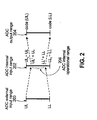
- FIG. 2 is a diagram illustrating a conventional external input range, an internal input range, and a compressed operational range of an analog-to-digital converter.
- FIG. 3 is a diagram illustrating an analog-to-digital conversion arrangement according to the present invention.
- FIG. 4 is a diagram illustrating another analog-to-digital conversion arrangement for converting a differential analog signal as an example for a better understanding of the invention.
- FIG. 5 is a diagram illustrating another examplary analog-to-digital conversion arrangement not covered by the claims.
- This invention proposes a more efficient solution to the three problems described above. It is quite often the case that these problems occur in a very narrow region near the LL I and UL I values.
- the size of the margins required to compensate for these problems at the LL I and UL I ends of the scale varies usually from a very small fraction of 1% to about 10% of full scale. For an optimal implementation it is thus desirable to be able to adjust the size of these margins with good resolution, repeatability and accuracy.
- FIG. 2 A graphical representation of the proposed relations between the external input range 200, the internal input range 202 and the output range 204 are shown in FIG. 2 . Furthermore, an operational range 206 that has been compressed from the internal input range is also shown.
- the maximum external input signal range LL - UL is compressed into a slightly smaller magnitude operational internal input range LL' - UL' 206 located within the internal maximum input range LL I - UL I .
- the maximum internal input range is approximately equal in size with the maximum external input range such that: LL ′ > LL I ⁇ LL and UL ′ ⁇ UL I ⁇ UL
- the output maximum range code(LL) - code(UL) is obtained by expanding the conversion engine output range code(LL') - code(UL').
- the ADC engine does not need to be over designed. Furthermore, the size of the margins maintained at the internal input range end points LL I and UL I can be precisely controlled by adjusting the input range compression ratio (LL-to-UL into LL'-to-UL') and its reciprocal - the output code expansion ratio (code(LL')-to-code(UL') into cade(LL)-to-cade(UL)).
- V RC LL ⁇ V RC ⁇ UL
- the compression factor resolution (through the ratio N1 / ( N + N1)) is directly dependent upon the oversampling ratio N and can be immediately improved by increasing this ratio.
- N1 / (N + N1) is preferably defined by digital control circuits, additional sources of inaccuracy are attributable solely to V RC . It is therefore desirable to derive V RC directly from the converter input range limit values LL and UL through digital relationships in order to minimize or eliminate additional sources of error.
- V RC 0.5*(LL + UL) can be done by sampling the LL external signal in half of the additional N1 sample periods and sampling the external UL signal in the remaining half. This would be particularly useful in a unipolar converter in which LL is usually ground and UL is usually the external reference voltage V REF .
- V RC value becomes zero and the range compression can be implemented by not sampling any voltage during the N1 additional periods (see FIG. 5 for such an example).
- An alternative implementation samples the -V REF external signal in half of the N1 periods and the +V REF external signal in the remaining half.
- V RC 0.75 * LL + 0.25 * UL as suggested in the second example presented above, one can elect to sample the LL external signal in three quarters of the additional N1 periods and the UL external signal in remaining one quarter of N1.
- the minimum condition for implementing range compression is an over-sampled ADC using N sample periods and having an input range LL-to-UL.
- a range compression signal V RC sampled as input during N1 additional sample periods.
- range compression can be obtained when the average V RC is between LL and UL.
- V RC signal is further desirable to derive the V RC signal from the LL and UL values, preferable through digital controlled relations.
- N R V AV / V REF * N
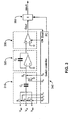
- the output comparator 330 generates the digital output stream Dout.
- This data stream is used by the switch controller 340 together with an internal clock signal to direct the operation of this first order over-sampling modulator.
- the proposed range compression is implemented within the switch controller 340 which is able to initiate three types of sampling cycles labeled IN, RP and RN.
- An IN-type sampling cycle is performed N times during a conversion operation and consists of sampling the analog input signal V IN .
- the modulator samples the upper reference input signal V RP or the lower reference input signal V RN depending upon the value of the Dout digital signal.
- the switch controller 340 preferably directs the following sequence of events:
- An RP-type sampling cycle is performed 0.5 * N1 times during a conversion operation and consists of sampling the upper reference input signal V RP .
- the modulator samples the upper reference input signal V RP or the lower reference input signal V RN depending upon the value of the Dout digital signal.
- the switch controller 340 directs the following sequence of events:
- the switch controller 340 must perform 2 16 IN-type sampling cycles, 32 RP-type sampling cycles and 32 RN-type sampling cycles during a complete conversion operation.
- the relative position of the RP and RN-type cycles within the IN-type cycles is chosen based upon previously described criteria.
- N 2 16
- the switch controller 340 will direct the succession of IN, RP and RN sampling cycles within one conversion operation as follow: a. Start the conversion operation. b. Set the accumulator within the digital filter 350 to initial value -32 and begin the accumulation of digital data Dout. c. Repeat 32 times the following steps 1 through 5. 1. Perform 512 IN-type cycles 2. Perform 1 RP-type cycle 3. Perform 1024 IN-type cycles 4. Perform 1 RN-type cycle 5. Perform 512 IN-type cycles d. End the accumulation process in filter 350 and output the conversion result e. End the conversion operation
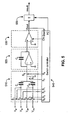
- FIG. 4 An example of a practical implementation not covered by the claims is shown in FIG. 4 .
- the converter receives a differential analog input signal [V IP , V IN ] and a differential analog reference signal [V RP , V RN ].
- the converter produces the digital output "result".
- FIG. 4 includes an input sampling circuit 410, an integrator 420, an output comparator 430 a switch controller 440 and a digital filter 450.
- the input sampling circuit contains an input sampling capacitor C I and a reference sampling capacitor C R . It receives two differential signals, the input signal [V IP , V IN ] and the reference signal [V RP , V RN ].
- the input differential signal [V IP , V IN ] connects to the input sampling capacitor C I through switch pair S1, S2.
- the reference differential signal [V RP , V RN ] connects to the input sampling capacitor C I through switch pair S3, S4 and to the reference sampling capacitor C R through switch pair S5, S6.
- the input sampling circuit 410 transfers the sampled signal to integrator 420 through switch S8.
- the integrator 420 accumulates the signal received from input sampling circuit 410 and drives the output comparator 430.
- the output data stream Dout is subsequently processed by a digital filter which reduces the shaped quantization noise and calculates the conversion result.
- the filter 450 is implemented as a simple digital accumulator with a sinc 1 frequency domain transfer function.
- the switch controller 440 through the signal FC frames the operation of the filter 450.
- the filter 450 will reset itself and accumulate the Dout data stream for N + N1 consecutive sample periods in order to produce one conversion result. Subsequently the accumulator will be reset again and the accumulation process restarted for a new conversion result.
- the differential reference signal [V RP , V RN ] defines, through the ratio of the input sampling capacitors C R / C I , the extent of the modulator external input range.
- the internal input range of this modulator is approximately equal to its external input range thus LL I ⁇ LL and UL I ⁇ UL.
- the slight differences between these values are due to offset and gain errors produced by real life performance limitations of the circuit elements used to implement this architecture. Such factors are amplifier offset and open-loop gain, switch charge injection and signal dependent parasitic impedances.
- [V IP , V IN ] represents the over-sampling converter differential analog input signal.
- the desired margins at the end points of the internal input range are both equal with approximately 0.048% of full scale.
- An RN-type sampling cycle is performed 0.5 * N1 times during a conversion operation and consists of sampling the inverse differential reference signal [V RN , V RP ] on input capacitor C I .
- the modulator will sample on reference capacitor C R the differential reference input signal [V RP , V RN] or the inverse differential reference input signal [V RN , V RP ] depending upon the value of the Dout digital signal.
- the switch controller 440 will direct the following sequence of events:
- An RN-type sampling cycle is performed 0.5 * N1 times during a conversion operation and consists of a null operation on input capacitor C I (i.e. no charge is sampled on input capacitor C I during and RP-type sampling cycle).
- the modulator will sample on reference capacitor C R the differential reference input signal [V RP , V RN] or the inverse differential reference input signal [V RN , V RP ] depending upon the value of the Dout digital signal.
- the switch controller 510 will direct the following sequence of events:
- This invention is immediately applicable to higher order modulators by increasing the complexity of the integrator stage, and can be integrated with other well known over-sampling converter architectures like band-pass, MASH, etc.
- the oversampling analog to digital converter according to the present application may comprise means which are adapted to carry out the before mentioned method steps.
Landscapes
- Engineering & Computer Science (AREA)
- Theoretical Computer Science (AREA)
- Analogue/Digital Conversion (AREA)
- Compression, Expansion, Code Conversion, And Decoders (AREA)
Claims (16)
- Procédé de conversion d'un signal d'entrée analogique asymétrique en un signal de sortie numérique au moyen d'un convertisseur analogique-numérique de suréchantillonnage, le procédé comprenant :- la réception du signal d'entrée analogique asymétrique (VIN) ;- la réception d'un premier signal de référence (VRN) et d'un second signal de référence (VRP) qui définissent une portée d'entrée externe du convertisseur ;- l'échantillonnage du signal d'entrée analogique asymétrique (VIN) N fois ;- la dérivée d'un signal de compression de portée (VRC) à partir des premier et second signaux de référence (VRN, VRP), le signal de compression de portée (VRC) ayant une amplitude qui est supérieure à l'amplitude du premier signal de référence (VRN) et inférieure à l'amplitude du second signal de référence (VRP)- l'échantillonnage du signal de compression de portée (VRC) N1 fois,- la réalisation de l'échantillonnage N fois et de l'échantillonnage N1 fois en une opération de conversion unique pour comprimer la portée d'entrée externe en une portée opérationnelle interne, dans lequel la compression se base en partie sur le rapport de N1/(N+N1), le signal d'entrée analogique asymétrique (VIN) et le signal de compression de portée (VRC) ; et- l'émission du signal de sortie numérique conformément aux signaux échantillonnés (VIN, VRC) réactifs à l'achèvement de l'échantillonnage N fois et de l'échantillonnage N1 fois.
- Procédé selon la revendication 1, comprenant en outre la compression d'une limite supérieure (UL) de la portée d'entrée externe en une limite supérieure (UL') de la portée opérationnelle interne.
- Procédé selon la revendication 1, comprenant en outre la compression d'une limite inférieure (LL) de la portée d'entrée externe en une limite inférieure (LL') de la portée opérationnelle interne.
- Procédé selon la revendication 1, comprenant en outre la compression de la portée d'entrée externe de sorte que la portée opérationnelle interne comprend un décalage proportionnel au signal de compression de portée (VRC).
- Procédé selon la revendication 1, comprenant en outre l'expansion du signal de sortie numérique du convertisseur analogique-numérique de sorte que le signal de sortie numérique (résultat) est indépendant du signal de compression de portée (VRC).
- Procédé selon la revendication 1, comprenant en outre l'expansion du signal de sortie numérique du convertisseur analogique-numérique de sorte que le signal de sortie numérique est indépendant de N1.
- Procédé selon la revendication 1, comprenant en outre la localisation de l'échantillonnage du signal de compression de portée (VRC) par rapport à l'échantillonnage du signal d'entrée analogique asymétrique (VIN) de manière à atténuer des composants de signal CA dans le signal de compression de portée (VRC).
- Procédé selon la revendication 1, comprenant en outre le fait de permettre un étalonnage final du convertisseur analogique-numérique.
- Convertisseur analogique-numérique de suréchantillonnage configuré pour convertir un signal d'entrée analogique asymétrique (VIN) en un signal de sortie numérique, le convertisseur analogique-numérique de suréchantillonnage comprenant :- un moyen de réception-- adapté à recevoir le signal d'entrée analogique asymétrique (VIN) ; et-- adapté à recevoir un premier signal de référence (VRN) et un second signal de référence (VRP) qui définissent une portée d'entrée externe du convertisseur ;- un moyen de dérivation adapté à dériver un signal de compression de portée (VRC) à partir des premier et second signaux de référence (VRN, VRP), le signal de compression de portée (VRC) ayant une amplitude qui est supérieure à l'amplitude du premier signal de référence (VRN) et inférieure à l'amplitude du second signal de référence (VRP);- un moyen d'échantillonnage-- adapté à échantillonner le signal d'entrée analogique asymétrique (VIN) N fois ;-- adapté à échantillonner le signal de compression de portée (VRC) N1 fois ; et-- adapté à réaliser l'échantillonnage N fois et l'échantillonnage N1 fois en une opération de conversion unique pour comprimer la portée d'entrée externe en une portée opérationnelle interne, dans lequel la compression se base en partie sur le rapport de N1/(N+N1), le signal d'entrée analogique asymétrique (VIN) et le signal de compression de portée (VRC) ; et- un moyen d'émission adapté à émettre le signal de sortie numérique conformément aux signaux échantillonnés (VIN, VRC) réactifs à l'achèvement de l'échantillonnage N fois et de l'échantillonnage N1 fois.
- Convertisseur selon la revendication 9, dans lequel le convertisseur comprend un circuit d'expansion qui est adapté de sorte que le signal de sortie numérique (résultat) est indépendant du signal de compression de portée (VRC).
- Convertisseur selon la revendication 9, dans lequel le convertisseur comprend un circuit d'expansion qui est adapté de sorte que le signal de sortie numérique (résultat) est indépendant de N1.
- Convertisseur selon la revendication 9, dans lequel le convertisseur est adapté de sorte que l'échantillonnage du signal de compression de portée (VRC) est localisé par rapport à l'échantillonnage du signal d'entrée analogique (VIN) de manière à atténuer des composants de signal CA dans le signal de compression de portée (VRC).
- Convertisseur selon la revendication 9, comprenant en outre un circuit d'expansion adapté à faire subir une expansion à la portée opérationnelle interne du convertisseur analogique-numérique pour obtenir une portée de sortie de signaux.
- Convertisseur selon la revendication 9, dans lequel le convertisseur comprend en outre un moyen de compression qui est adapté à comprimer une limite supérieure (UL) de la portée d'entrée externe en une limite supérieure (UL') de la portée opérationnelle interne.
- Convertisseur selon la revendication 9, dans lequel le convertisseur comprend en outre un moyen de compression qui est adapté à comprimer une limite inférieure (LL) de la portée d'entrée externe en une limite inférieure (LL') de la portée opérationnelle interne.
- Convertisseur selon la revendication 9, dans lequel le convertisseur comprend en outre un moyen de compression qui est adapté à comprimer la portée d'entrée externe de sorte que la portée opérationnelle interne comprend un décalage proportionnel au signal de compression de portée (VRC).
Applications Claiming Priority (1)
| Application Number | Priority Date | Filing Date | Title |
|---|---|---|---|
| US11/483,420 US7348907B2 (en) | 2006-07-07 | 2006-07-07 | Range compression in oversampling analog-to-digital converters |
Publications (3)
| Publication Number | Publication Date |
|---|---|
| EP1903683A2 EP1903683A2 (fr) | 2008-03-26 |
| EP1903683A3 EP1903683A3 (fr) | 2009-06-10 |
| EP1903683B1 true EP1903683B1 (fr) | 2011-11-30 |
Family
ID=38617223
Family Applications (1)
| Application Number | Title | Priority Date | Filing Date |
|---|---|---|---|
| EP07111882A Ceased EP1903683B1 (fr) | 2006-07-07 | 2007-07-05 | Compression de portée pour le suréchantillonnage de convertisseurs analogiques-numériques |
Country Status (3)
| Country | Link |
|---|---|
| US (1) | US7348907B2 (fr) |
| EP (1) | EP1903683B1 (fr) |
| TW (1) | TWI426716B (fr) |
Families Citing this family (2)
| Publication number | Priority date | Publication date | Assignee | Title |
|---|---|---|---|---|
| US7397403B2 (en) * | 2006-07-07 | 2008-07-08 | Linear Technology Corp. | Range compression in oversampling analog-to-digital converters using differential input signals |
| CN104318888B (zh) * | 2014-11-06 | 2017-09-15 | 京东方科技集团股份有限公司 | 阵列基板栅极驱动单元、方法、电路和显示装置 |
Family Cites Families (13)
| Publication number | Priority date | Publication date | Assignee | Title |
|---|---|---|---|---|
| US5187482A (en) * | 1992-03-02 | 1993-02-16 | General Electric Company | Delta sigma analog-to-digital converter with increased dynamic range |
| JPH06180948A (ja) * | 1992-12-11 | 1994-06-28 | Sony Corp | ディジタル信号処理装置又は方法、及び記録媒体 |
| US5706352A (en) * | 1993-04-07 | 1998-01-06 | K/S Himpp | Adaptive gain and filtering circuit for a sound reproduction system |
| US5539202A (en) * | 1994-10-03 | 1996-07-23 | Adac Laboratories, Inc. | Modifiable digital dynamic compression table |
| US6097824A (en) * | 1997-06-06 | 2000-08-01 | Audiologic, Incorporated | Continuous frequency dynamic range audio compressor |
| US5832444A (en) * | 1996-09-10 | 1998-11-03 | Schmidt; Jon C. | Apparatus for dynamic range compression of an audio signal |
| US6140950A (en) | 1998-08-17 | 2000-10-31 | Linear Technology Corporation | Delta-sigma modulator with improved full-scale accuracy |
| US6169506B1 (en) | 1998-08-17 | 2001-01-02 | Linear Technology Corp. | Oversampling data converter with good rejection capability |
| US6493657B1 (en) * | 1999-08-20 | 2002-12-10 | Glp Partnership | Amplitude range matching system |
| US6628216B2 (en) * | 2002-02-13 | 2003-09-30 | Intersil Americas Inc. | Calibration of resistor ladder using difference measurement and parallel resistive correction |
| US7046046B2 (en) * | 2004-03-23 | 2006-05-16 | Microchip Technology Incorporated | Switched capacitor signal scaling circuit |
| US7222037B2 (en) * | 2004-10-15 | 2007-05-22 | Genesis Microchip Inc. | Hybrid automatic gain control (AGC) |
| US8605836B2 (en) * | 2005-03-11 | 2013-12-10 | Qualcomm Incorporated | Automatic gain control for a wireless receiver |
-
2006
- 2006-07-07 US US11/483,420 patent/US7348907B2/en active Active
-
2007
- 2007-07-05 EP EP07111882A patent/EP1903683B1/fr not_active Ceased
- 2007-07-06 TW TW096124806A patent/TWI426716B/zh not_active IP Right Cessation
Also Published As
| Publication number | Publication date |
|---|---|
| US20080007435A1 (en) | 2008-01-10 |
| US7348907B2 (en) | 2008-03-25 |
| EP1903683A3 (fr) | 2009-06-10 |
| TW200826515A (en) | 2008-06-16 |
| EP1903683A2 (fr) | 2008-03-26 |
| TWI426716B (zh) | 2014-02-11 |
Similar Documents
| Publication | Publication Date | Title |
|---|---|---|
| Breems et al. | A cascaded continuous-time/spl Sigma//spl Delta/Modulator with 67-dB dynamic range in 10-MHz bandwidth | |
| US5055843A (en) | Sigma delta modulator with distributed prefiltering and feedback | |
| Del Signore et al. | A monolithic 2-b delta-sigma A/D converter | |
| JP3530587B2 (ja) | 可変利得入力ステージを備える信号処理回路 | |
| JP5154659B2 (ja) | フィードバックパスにおいてビット数の減少したマルチビットシグマ・デルタ変調器 | |
| CN101375507B (zh) | 具有用于rc分布补偿的电容和/或电阻数字自校准装置的连续时间sigma-delta模数转换器 | |
| EP1777825B1 (fr) | Modulateur Delta-Sigma basé sur filtre passe-bas | |
| US6922161B2 (en) | Delta-Sigma modulator for reducing quantization noise and oversampling ratio (OSR) | |
| US8223051B2 (en) | Multi-bit sigma-delta modulator with reduced number of bits in feedback path | |
| US20050068213A1 (en) | Digital compensation of excess delay in continuous time sigma delta modulators | |
| US8970412B2 (en) | Signal quantization method and apparatus and sensor based thereon | |
| US11251807B1 (en) | Wide bandwidth ADC with inherent anti-aliasing and high DC precision | |
| US7084791B2 (en) | Analog-to-digital converter with correction of offset errors | |
| US11626885B1 (en) | Gain programmability techniques for delta-sigma analog-to-digital converter | |
| US10116324B2 (en) | High-linearity sigma-delta converter | |
| Markus et al. | Incremental delta-sigma structures for DC measurement: An overview | |
| AU2182100A (en) | Method and apparatus for eliminating clock jitter in continuous-time delta-sigma analog-to-digital converters | |
| US10153778B2 (en) | High-linearity sigma-delta converter | |
| EP1876715B1 (fr) | Compression de portée pour le suréchantillonnage de convertisseurs analogiques-numériques utilisant des signaux d'entrée différentiels | |
| EP3955467A1 (fr) | Convertisseur analogique-numérique sigma-delta à plusieurs étages avec tremblement | |
| EP1903683B1 (fr) | Compression de portée pour le suréchantillonnage de convertisseurs analogiques-numériques | |
| US6522276B2 (en) | System of DAC correction for a ΔΣ modulator | |
| US11621722B2 (en) | Multi quantizer loops for delta-sigma converters | |
| Ortmanns et al. | Successful design of cascaded continuous-time/spl Sigma//spl Delta/modulators | |
| Hsieh et al. | A sar-assisted continuous-time incremental σδ adc with first-order noise coupling |
Legal Events
| Date | Code | Title | Description |
|---|---|---|---|
| PUAI | Public reference made under article 153(3) epc to a published international application that has entered the european phase |
Free format text: ORIGINAL CODE: 0009012 |
|
| AK | Designated contracting states |
Kind code of ref document: A2 Designated state(s): AT BE BG CH CY CZ DE DK EE ES FI FR GB GR HU IE IS IT LI LT LU LV MC MT NL PL PT RO SE SI SK TR |
|
| AX | Request for extension of the european patent |
Extension state: AL BA HR MK YU |
|
| PUAL | Search report despatched |
Free format text: ORIGINAL CODE: 0009013 |
|
| AK | Designated contracting states |
Kind code of ref document: A3 Designated state(s): AT BE BG CH CY CZ DE DK EE ES FI FR GB GR HU IE IS IT LI LT LU LV MC MT NL PL PT RO SE SI SK TR |
|
| AX | Request for extension of the european patent |
Extension state: AL BA HR MK RS |
|
| 17P | Request for examination filed |
Effective date: 20091019 |
|
| 17Q | First examination report despatched |
Effective date: 20091112 |
|
| AKX | Designation fees paid |
Designated state(s): DE FR GB IT NL |
|
| GRAP | Despatch of communication of intention to grant a patent |
Free format text: ORIGINAL CODE: EPIDOSNIGR1 |
|
| RAP1 | Party data changed (applicant data changed or rights of an application transferred) |
Owner name: LINEAR TECHNOLOGY CORPORATION |
|
| GRAS | Grant fee paid |
Free format text: ORIGINAL CODE: EPIDOSNIGR3 |
|
| GRAA | (expected) grant |
Free format text: ORIGINAL CODE: 0009210 |
|
| AK | Designated contracting states |
Kind code of ref document: B1 Designated state(s): DE FR GB IT NL |
|
| REG | Reference to a national code |
Ref country code: GB Ref legal event code: FG4D |
|
| REG | Reference to a national code |
Ref country code: DE Ref legal event code: R096 Ref document number: 602007019023 Country of ref document: DE Effective date: 20120202 |
|
| REG | Reference to a national code |
Ref country code: NL Ref legal event code: T3 |
|
| PLBE | No opposition filed within time limit |
Free format text: ORIGINAL CODE: 0009261 |
|
| STAA | Information on the status of an ep patent application or granted ep patent |
Free format text: STATUS: NO OPPOSITION FILED WITHIN TIME LIMIT |
|
| 26N | No opposition filed |
Effective date: 20120831 |
|
| REG | Reference to a national code |
Ref country code: DE Ref legal event code: R097 Ref document number: 602007019023 Country of ref document: DE Effective date: 20120831 |
|
| REG | Reference to a national code |
Ref country code: FR Ref legal event code: PLFP Year of fee payment: 10 |
|
| REG | Reference to a national code |
Ref country code: FR Ref legal event code: PLFP Year of fee payment: 11 |
|
| REG | Reference to a national code |
Ref country code: FR Ref legal event code: PLFP Year of fee payment: 12 |
|
| REG | Reference to a national code |
Ref country code: DE Ref legal event code: R082 Ref document number: 602007019023 Country of ref document: DE Representative=s name: MUELLER-BORE & PARTNER PATENTANWAELTE PARTG MB, DE Ref country code: DE Ref legal event code: R081 Ref document number: 602007019023 Country of ref document: DE Owner name: ANALOG DEVICES INTERNATIONAL UNLIMITED COMPANY, IE Free format text: FORMER OWNER: LINEAR TECHNOLOGY CORPORATION, MILPITAS, CALIF., US Ref country code: DE Ref legal event code: R082 Ref document number: 602007019023 Country of ref document: DE Representative=s name: WITHERS & ROGERS LLP, DE |
|
| REG | Reference to a national code |
Ref country code: DE Ref legal event code: R082 Ref document number: 602007019023 Country of ref document: DE Representative=s name: WITHERS & ROGERS LLP, DE |
|
| PGFP | Annual fee paid to national office [announced via postgrant information from national office to epo] |
Ref country code: NL Payment date: 20210622 Year of fee payment: 15 Ref country code: IT Payment date: 20210622 Year of fee payment: 15 Ref country code: FR Payment date: 20210623 Year of fee payment: 15 |
|
| PGFP | Annual fee paid to national office [announced via postgrant information from national office to epo] |
Ref country code: GB Payment date: 20210623 Year of fee payment: 15 |
|
| REG | Reference to a national code |
Ref country code: GB Ref legal event code: 732E Free format text: REGISTERED BETWEEN 20210930 AND 20211006 |
|
| PGFP | Annual fee paid to national office [announced via postgrant information from national office to epo] |
Ref country code: DE Payment date: 20210622 Year of fee payment: 15 |
|
| REG | Reference to a national code |
Ref country code: NL Ref legal event code: PD Owner name: ANALOG DEVICES INTERNATIONAL UNLIMITED COMPANY; IE Free format text: DETAILS ASSIGNMENT: CHANGE OF OWNER(S), ASSIGNMENT; FORMER OWNER NAME: LINEAR TECHNOLOGY LLC Effective date: 20211216 |
|
| REG | Reference to a national code |
Ref country code: DE Ref legal event code: R119 Ref document number: 602007019023 Country of ref document: DE |
|
| REG | Reference to a national code |
Ref country code: NL Ref legal event code: MM Effective date: 20220801 |
|
| GBPC | Gb: european patent ceased through non-payment of renewal fee |
Effective date: 20220705 |
|
| PG25 | Lapsed in a contracting state [announced via postgrant information from national office to epo] |
Ref country code: FR Free format text: LAPSE BECAUSE OF NON-PAYMENT OF DUE FEES Effective date: 20220731 |
|
| PG25 | Lapsed in a contracting state [announced via postgrant information from national office to epo] |
Ref country code: GB Free format text: LAPSE BECAUSE OF NON-PAYMENT OF DUE FEES Effective date: 20220705 Ref country code: DE Free format text: LAPSE BECAUSE OF NON-PAYMENT OF DUE FEES Effective date: 20230201 |
|
| PG25 | Lapsed in a contracting state [announced via postgrant information from national office to epo] |
Ref country code: NL Free format text: LAPSE BECAUSE OF NON-PAYMENT OF DUE FEES Effective date: 20220801 |
|
| PG25 | Lapsed in a contracting state [announced via postgrant information from national office to epo] |
Ref country code: IT Free format text: LAPSE BECAUSE OF NON-PAYMENT OF DUE FEES Effective date: 20220705 |