EP1905077B1 - Dispositif à semi-conducteur - Google Patents
Dispositif à semi-conducteur Download PDFInfo
- Publication number
- EP1905077B1 EP1905077B1 EP06766009A EP06766009A EP1905077B1 EP 1905077 B1 EP1905077 B1 EP 1905077B1 EP 06766009 A EP06766009 A EP 06766009A EP 06766009 A EP06766009 A EP 06766009A EP 1905077 B1 EP1905077 B1 EP 1905077B1
- Authority
- EP
- European Patent Office
- Prior art keywords
- die
- die pad
- surface portion
- semi
- top surface
- Prior art date
- Legal status (The legal status is an assumption and is not a legal conclusion. Google has not performed a legal analysis and makes no representation as to the accuracy of the status listed.)
- Not-in-force
Links
Images


Classifications
-
- H—ELECTRICITY
- H10—SEMICONDUCTOR DEVICES; ELECTRIC SOLID-STATE DEVICES NOT OTHERWISE PROVIDED FOR
- H10W—GENERIC PACKAGES, INTERCONNECTIONS, CONNECTORS OR OTHER CONSTRUCTIONAL DETAILS OF DEVICES COVERED BY CLASS H10
- H10W70/00—Package substrates; Interposers; Redistribution layers [RDL]
- H10W70/40—Leadframes
- H10W70/411—Chip-supporting parts, e.g. die pads
-
- H—ELECTRICITY
- H10—SEMICONDUCTOR DEVICES; ELECTRIC SOLID-STATE DEVICES NOT OTHERWISE PROVIDED FOR
- H10W—GENERIC PACKAGES, INTERCONNECTIONS, CONNECTORS OR OTHER CONSTRUCTIONAL DETAILS OF DEVICES COVERED BY CLASS H10
- H10W42/00—Arrangements for protection of devices
- H10W42/121—Arrangements for protection of devices protecting against mechanical damage
-
- H—ELECTRICITY
- H10—SEMICONDUCTOR DEVICES; ELECTRIC SOLID-STATE DEVICES NOT OTHERWISE PROVIDED FOR
- H10W—GENERIC PACKAGES, INTERCONNECTIONS, CONNECTORS OR OTHER CONSTRUCTIONAL DETAILS OF DEVICES COVERED BY CLASS H10
- H10W70/00—Package substrates; Interposers; Redistribution layers [RDL]
- H10W70/60—Insulating or insulated package substrates; Interposers; Redistribution layers
- H10W70/67—Insulating or insulated package substrates; Interposers; Redistribution layers characterised by their insulating layers or insulating parts
- H10W70/68—Shapes or dispositions thereof
- H10W70/682—Shapes or dispositions thereof comprising holes having chips therein
-
- H—ELECTRICITY
- H10—SEMICONDUCTOR DEVICES; ELECTRIC SOLID-STATE DEVICES NOT OTHERWISE PROVIDED FOR
- H10W—GENERIC PACKAGES, INTERCONNECTIONS, CONNECTORS OR OTHER CONSTRUCTIONAL DETAILS OF DEVICES COVERED BY CLASS H10
- H10W72/00—Interconnections or connectors in packages
- H10W72/01—Manufacture or treatment
- H10W72/013—Manufacture or treatment of die-attach connectors
- H10W72/01308—Manufacture or treatment of die-attach connectors using permanent auxiliary members, e.g. using alignment marks
-
- H—ELECTRICITY
- H10—SEMICONDUCTOR DEVICES; ELECTRIC SOLID-STATE DEVICES NOT OTHERWISE PROVIDED FOR
- H10W—GENERIC PACKAGES, INTERCONNECTIONS, CONNECTORS OR OTHER CONSTRUCTIONAL DETAILS OF DEVICES COVERED BY CLASS H10
- H10W72/00—Interconnections or connectors in packages
- H10W72/071—Connecting or disconnecting
- H10W72/073—Connecting or disconnecting of die-attach connectors
- H10W72/07311—Treating the bonding area before connecting, e.g. by applying flux or cleaning
-
- H—ELECTRICITY
- H10—SEMICONDUCTOR DEVICES; ELECTRIC SOLID-STATE DEVICES NOT OTHERWISE PROVIDED FOR
- H10W—GENERIC PACKAGES, INTERCONNECTIONS, CONNECTORS OR OTHER CONSTRUCTIONAL DETAILS OF DEVICES COVERED BY CLASS H10
- H10W72/00—Interconnections or connectors in packages
- H10W72/071—Connecting or disconnecting
- H10W72/074—Connecting or disconnecting of anisotropic conductive adhesives
-
- H—ELECTRICITY
- H10—SEMICONDUCTOR DEVICES; ELECTRIC SOLID-STATE DEVICES NOT OTHERWISE PROVIDED FOR
- H10W—GENERIC PACKAGES, INTERCONNECTIONS, CONNECTORS OR OTHER CONSTRUCTIONAL DETAILS OF DEVICES COVERED BY CLASS H10
- H10W72/00—Interconnections or connectors in packages
- H10W72/071—Connecting or disconnecting
- H10W72/075—Connecting or disconnecting of bond wires
- H10W72/07511—Treating the bonding area before connecting, e.g. by applying flux or cleaning
-
- H—ELECTRICITY
- H10—SEMICONDUCTOR DEVICES; ELECTRIC SOLID-STATE DEVICES NOT OTHERWISE PROVIDED FOR
- H10W—GENERIC PACKAGES, INTERCONNECTIONS, CONNECTORS OR OTHER CONSTRUCTIONAL DETAILS OF DEVICES COVERED BY CLASS H10
- H10W72/00—Interconnections or connectors in packages
- H10W72/30—Die-attach connectors
- H10W72/321—Structures or relative sizes of die-attach connectors
- H10W72/325—Die-attach connectors having a filler embedded in a matrix
-
- H—ELECTRICITY
- H10—SEMICONDUCTOR DEVICES; ELECTRIC SOLID-STATE DEVICES NOT OTHERWISE PROVIDED FOR
- H10W—GENERIC PACKAGES, INTERCONNECTIONS, CONNECTORS OR OTHER CONSTRUCTIONAL DETAILS OF DEVICES COVERED BY CLASS H10
- H10W72/00—Interconnections or connectors in packages
- H10W72/30—Die-attach connectors
- H10W72/351—Materials of die-attach connectors
- H10W72/352—Materials of die-attach connectors comprising metals or metalloids, e.g. solders
-
- H—ELECTRICITY
- H10—SEMICONDUCTOR DEVICES; ELECTRIC SOLID-STATE DEVICES NOT OTHERWISE PROVIDED FOR
- H10W—GENERIC PACKAGES, INTERCONNECTIONS, CONNECTORS OR OTHER CONSTRUCTIONAL DETAILS OF DEVICES COVERED BY CLASS H10
- H10W72/00—Interconnections or connectors in packages
- H10W72/30—Die-attach connectors
- H10W72/351—Materials of die-attach connectors
- H10W72/353—Materials of die-attach connectors not comprising solid metals or solid metalloids, e.g. ceramics
- H10W72/354—Materials of die-attach connectors not comprising solid metals or solid metalloids, e.g. ceramics comprising polymers
-
- H—ELECTRICITY
- H10—SEMICONDUCTOR DEVICES; ELECTRIC SOLID-STATE DEVICES NOT OTHERWISE PROVIDED FOR
- H10W—GENERIC PACKAGES, INTERCONNECTIONS, CONNECTORS OR OTHER CONSTRUCTIONAL DETAILS OF DEVICES COVERED BY CLASS H10
- H10W72/00—Interconnections or connectors in packages
- H10W72/50—Bond wires
- H10W72/531—Shapes of wire connectors
- H10W72/536—Shapes of wire connectors the connected ends being ball-shaped
-
- H—ELECTRICITY
- H10—SEMICONDUCTOR DEVICES; ELECTRIC SOLID-STATE DEVICES NOT OTHERWISE PROVIDED FOR
- H10W—GENERIC PACKAGES, INTERCONNECTIONS, CONNECTORS OR OTHER CONSTRUCTIONAL DETAILS OF DEVICES COVERED BY CLASS H10
- H10W72/00—Interconnections or connectors in packages
- H10W72/50—Bond wires
- H10W72/531—Shapes of wire connectors
- H10W72/5363—Shapes of wire connectors the connected ends being wedge-shaped
-
- H—ELECTRICITY
- H10—SEMICONDUCTOR DEVICES; ELECTRIC SOLID-STATE DEVICES NOT OTHERWISE PROVIDED FOR
- H10W—GENERIC PACKAGES, INTERCONNECTIONS, CONNECTORS OR OTHER CONSTRUCTIONAL DETAILS OF DEVICES COVERED BY CLASS H10
- H10W72/00—Interconnections or connectors in packages
- H10W72/50—Bond wires
- H10W72/541—Dispositions of bond wires
- H10W72/5434—Dispositions of bond wires the connected ends being on auxiliary connecting means on bond pads, e.g. on other bond wires
-
- H—ELECTRICITY
- H10—SEMICONDUCTOR DEVICES; ELECTRIC SOLID-STATE DEVICES NOT OTHERWISE PROVIDED FOR
- H10W—GENERIC PACKAGES, INTERCONNECTIONS, CONNECTORS OR OTHER CONSTRUCTIONAL DETAILS OF DEVICES COVERED BY CLASS H10
- H10W72/00—Interconnections or connectors in packages
- H10W72/50—Bond wires
- H10W72/551—Materials of bond wires
- H10W72/552—Materials of bond wires comprising metals or metalloids, e.g. silver
- H10W72/5522—Materials of bond wires comprising metals or metalloids, e.g. silver comprising gold [Au]
-
- H—ELECTRICITY
- H10—SEMICONDUCTOR DEVICES; ELECTRIC SOLID-STATE DEVICES NOT OTHERWISE PROVIDED FOR
- H10W—GENERIC PACKAGES, INTERCONNECTIONS, CONNECTORS OR OTHER CONSTRUCTIONAL DETAILS OF DEVICES COVERED BY CLASS H10
- H10W72/00—Interconnections or connectors in packages
- H10W72/50—Bond wires
- H10W72/59—Bond pads specially adapted therefor
-
- H—ELECTRICITY
- H10—SEMICONDUCTOR DEVICES; ELECTRIC SOLID-STATE DEVICES NOT OTHERWISE PROVIDED FOR
- H10W—GENERIC PACKAGES, INTERCONNECTIONS, CONNECTORS OR OTHER CONSTRUCTIONAL DETAILS OF DEVICES COVERED BY CLASS H10
- H10W72/00—Interconnections or connectors in packages
- H10W72/851—Dispositions of multiple connectors or interconnections
- H10W72/874—On different surfaces
- H10W72/884—Die-attach connectors and bond wires
-
- H—ELECTRICITY
- H10—SEMICONDUCTOR DEVICES; ELECTRIC SOLID-STATE DEVICES NOT OTHERWISE PROVIDED FOR
- H10W—GENERIC PACKAGES, INTERCONNECTIONS, CONNECTORS OR OTHER CONSTRUCTIONAL DETAILS OF DEVICES COVERED BY CLASS H10
- H10W72/00—Interconnections or connectors in packages
- H10W72/90—Bond pads, in general
- H10W72/931—Shapes of bond pads
-
- H—ELECTRICITY
- H10—SEMICONDUCTOR DEVICES; ELECTRIC SOLID-STATE DEVICES NOT OTHERWISE PROVIDED FOR
- H10W—GENERIC PACKAGES, INTERCONNECTIONS, CONNECTORS OR OTHER CONSTRUCTIONAL DETAILS OF DEVICES COVERED BY CLASS H10
- H10W74/00—Encapsulations, e.g. protective coatings
-
- H—ELECTRICITY
- H10—SEMICONDUCTOR DEVICES; ELECTRIC SOLID-STATE DEVICES NOT OTHERWISE PROVIDED FOR
- H10W—GENERIC PACKAGES, INTERCONNECTIONS, CONNECTORS OR OTHER CONSTRUCTIONAL DETAILS OF DEVICES COVERED BY CLASS H10
- H10W74/00—Encapsulations, e.g. protective coatings
- H10W74/10—Encapsulations, e.g. protective coatings characterised by their shape or disposition
- H10W74/111—Encapsulations, e.g. protective coatings characterised by their shape or disposition the semiconductor body being completely enclosed
- H10W74/127—Encapsulations, e.g. protective coatings characterised by their shape or disposition the semiconductor body being completely enclosed characterised by arrangements for sealing or adhesion
-
- H—ELECTRICITY
- H10—SEMICONDUCTOR DEVICES; ELECTRIC SOLID-STATE DEVICES NOT OTHERWISE PROVIDED FOR
- H10W—GENERIC PACKAGES, INTERCONNECTIONS, CONNECTORS OR OTHER CONSTRUCTIONAL DETAILS OF DEVICES COVERED BY CLASS H10
- H10W90/00—Package configurations
- H10W90/701—Package configurations characterised by the relative positions of pads or connectors relative to package parts
- H10W90/731—Package configurations characterised by the relative positions of pads or connectors relative to package parts of die-attach connectors
- H10W90/736—Package configurations characterised by the relative positions of pads or connectors relative to package parts of die-attach connectors between a chip and a stacked lead frame, conducting package substrate or heat sink
-
- H—ELECTRICITY
- H10—SEMICONDUCTOR DEVICES; ELECTRIC SOLID-STATE DEVICES NOT OTHERWISE PROVIDED FOR
- H10W—GENERIC PACKAGES, INTERCONNECTIONS, CONNECTORS OR OTHER CONSTRUCTIONAL DETAILS OF DEVICES COVERED BY CLASS H10
- H10W90/00—Package configurations
- H10W90/701—Package configurations characterised by the relative positions of pads or connectors relative to package parts
- H10W90/751—Package configurations characterised by the relative positions of pads or connectors relative to package parts of bond wires
- H10W90/756—Package configurations characterised by the relative positions of pads or connectors relative to package parts of bond wires between a chip and a stacked lead frame, conducting package substrate or heat sink
Definitions
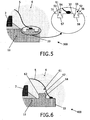
- Figure 2 on a larger scale, illustrates two mechanisms that are considered to be probably responsible for a large percentage of the failure of the downbonds 5.
- the plastic may directly exert forces on the downbond wires 5.
- delamination may occur at the interface between die 2 and die pad 11, and this delamination, which may be considered as a creeping crack, may increase along the top surface 15 of the die pad 11, as indicated at 23.
- a downbond 5 may break (metal fatigue, and/or tear), as indicated at 24.
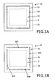
- Figure 3 is a view comparable to Figure 2 , illustrating a detail (not to scale) of a preferred embodiment of semi-conductor device 100 according to the present invention.
- undercutting 16 is not shown for sake of simplicity, but such undercutting will preferably be present, indeed.
- the leadframe 10 is made starting from a standard solid flat strip of a predetermined thickness, typically approximately 0.2 mm In this strip, an array of leadframes is formed by etching; in a later stage, the individual leadframes are separated from each other by a sawing process.
- the ridge 61 may extend as a closed loop around the die 2, or the ridge 61 may comprise a series of elevated portions. Also, two parallel ridges may be present in the region between the die attachment surface portion 31 and the downbond attachment surface portion 32 (not shown). Also, a second ridge may be present in the region between the downbond attachment surface portion 32 and the side edge 33 of the die pad 11 (not shown).
Landscapes
- Lead Frames For Integrated Circuits (AREA)
- Structures Or Materials For Encapsulating Or Coating Semiconductor Devices Or Solid State Devices (AREA)
- Die Bonding (AREA)
- Wire Bonding (AREA)
Abstract
Claims (13)
- Grille de connexion (10) pour un dispositif à semi-conducteurs, comprenant une plaquette de puce (11) pour le montage d'une puce de semi-conducteurs (2) et une pluralité de conducteurs (12) pour la connexion avec la puce de semi-conducteurs (2), les conducteurs étant disposés à une certaine distance de la puce de semi-conducteurs (11) ;
dans laquelle la plaquette de puce (11) a une surface inférieure plate (14) s'étendant selon un plan unique sur la totalité de l'extension de la plaquette pour recevoir la puce, et une surface supérieure (15), la surface supérieure (15) ayant une partie de fixation de la puce (31) et une partie de fixation d'interconnexions inférieures (32) pour le raccordement d'interconnexions inférieures (5) ;
dans laquelle, à au moins un emplacement entre la partie de fixation de la puce (31) et la partie de fixation d'interconnexions inférieures (32), la surface supérieure (15) de la plaquette de puce (11) a au moins une troisième partie de surface qui est hors du plan par rapport à la partie de fixation de la puce (31), et au moins une transition de surface substantiellement en forme d'échelon (36 ; 43 ; 53 ; 63) entre la partie de fixation de la puce (31) et ladite troisième partie de surface,
et dans laquelle, à un emplacement entre la partie de fixation de la puce (31) et la partie de fixation d'interconnexions inférieures (32), la plaquette de puce (11) a :au moins une partie en retrait (34 ; 41, 42 ; 51) dans sa surface supérieure (15), dans laquelle ladite troisième partie de surface (35 ; 47, 48 ; 57) est définie par un fond de ladite partie en retrait, et dans laquelle ladite transition en forme d'échelon (36 ; 43 ; 53 ; 63) est définie par une paroi de ladite partie en retrait ; ouau moins une nervure (61) dans sa surface supérieure (15), dans laquelle ladite troisième partie de surface (62) est définie par un sommet de ladite nervure et dans laquelle ladite transition en forme d'échelon (63, 64) est définie par une paroi de ladite nervure (61). - Grille de connexion selon la revendication 1, dans laquelle ladite transition a été formée par l'élimination, par gravure, d'une partie de la surface supérieure.
- Grille de connexion selon l'une quelconque des revendications précédentes, dans laquelle la plaquette de puce a au moins une partie en retrait, et dans laquelle ladite partie en retrait (34 ; 41, 42 ; 51) est formée par une rainure dirigée de manière substantiellement parallèle à un bord latéral (33) de la plaquette de puce (11).
- Grille de connexion selon la revendication 3, dans laquelle ladite rainure (34) est une rainure annulaire fermée sur elle-même de forme substantiellement rectangulaire, correspondant à la forme de la plaquette de puce (11).
- Grille de connexion selon l'une quelconque des revendications précédentes, dans laquelle la plaquette de puce a au moins une partie en retrait, et dans laquelle ladite partie en retrait (34 ; 41, 42 ; 51) a un contour de section transversale substantiellement rectangulaire.
- Grille de connexion selon l'une quelconque des revendications précédentes, dans laquelle la partie de fixation d'interconnexions inférieures (32) est alignée avec la partie de fixation de la puce (31).
- Grille de connexion selon l'une quelconque des revendications précédentes, dans laquelle la plaquette de puce (11) a au moins une autre partie en retrait (52) dans sa surface supérieure (15), à un emplacement situé entre la partie de fixation d'interconnexions inférieures (32) et un bord latéral (33) de la plaquette de puce (11).
- Grille de connexion selon l'une quelconque des revendications précédentes, dans laquelle la plaquette de puce a au moins une nervure, et dans laquelle ladite nervure (61) a été formée par l'élimination, par gravure, de parties du matériau de base de la grille de connexion pour former la partie de fixation de la puce (31) et la partie de fixation d'interconnexions inférieures (32), respectivement.
- Dispositif à semi-conducteurs, comprenant :une grille de connexion (10) selon la revendication 1 ;une puce de semi-conducteurs (2) fixée à la partie de fixation de la puce (31) de la plaquette de puce (11), la puce de semi-conducteur (2) contenant un circuit intégré ;une pluralité d'interconnexions normales (4) connectant ledit circuit intégré aux conducteurs respectifs (12) ;une pluralité d'interconnexions inférieures (5) raccordant ledit circuit intégré à la partie de fixation d'interconnexions inférieures (32) de la plaquette de puce (11) ; etun boîtier en plastique (6) encapsulant au moins la puce de semi-conducteurs (2), les interconnexions normales (4) et les interconnexions inférieures (5).
- Dispositif à semi-conducteurs selon la revendication 9, dans lequel la grille de connexion (10) est exposée.
- Dispositif à semi-conducteurs selon la revendication 9, avec une grille de connexion (10) selon la revendication 1, dans lequel la plaquette de puce a la au moins une partie en retrait, et dans lequel ladite au moins une partie en retrait (34 ; 41, 42 ; 51) est entièrement remplie avec le matériau plastique de l'encapsulation (6).
- Procédé de fabrication d'un dispositif à semi-conducteurs, le procédé comprenant les étapes de :mettre en place d'une bande de grille de connexion de base ;à l'aide d'un procédé de gravure, définir au moins une grille de connexion (10), comprenant une plaquette de puce (11) et une pluralité de conducteurs (12), dans lequel la plaquette de puce (11) a une surface inférieure plate (14), s'étendant selon un plan unique sur la totalité de la plaquette de puce, et une surface supérieure (15), la surface supérieure (15) ayant une partie de fixation de la puce (31) et une partie de fixation d'interconnexions inférieures (32) pour le raccordement des interconnexions inférieures (5) ;à l'aide d'un procédé de gravure, éliminer au moins une partie de la surface supérieure (15) de la plaquette de puce (11), à au moins un emplacement entre la partie de surface de fixation de la puce (31) et la partie de surface de fixation d'interconnexions inférieures (32), afin de définir au moins une troisième partie de surface qui est hors du plan par rapport à la partie de surface de fixation de la puce (31), et au moins une transition de surface substantiellement en forme d'échelon (36 ; 43 ; 53 ; 63) entre la partie de surface de fixation de la puce (31) et ladite troisième partie de surface, de telle sorte que, en au moins un emplacement la plaquette de puce a (11) :au moins une partie en retrait (34 ; 41, 42 ; 51) dans sa surface supérieure (15), dans lequel ladite troisième partie de surface (35 ; 47, 48 ; 57) est définie par un fond de ladite partie en retrait, et dans lequel ladite transition en forme d'échelon (36 ; 43 ; 53 ; 63) est définie par une paroi de ladite partie en retrait ; ouau moins une nervure (61) sur sa surface supérieure (15), dans lequel ladite troisième partie de surface (62) est définie par un sommet de ladite nervure et dans lequel ladite transition en forme d'échelon (63, 64) est définie par une paroi de ladite nervure (61) ;fixer une puce de semi-conducteurs (2) à la partie de fixation de la puce (31) de la plaquette de puce (11), la puce de semi-conducteurs (2) comprenant un circuit intégré ;connecter des interconnexions normales (4) audit circuit intégré et aux conducteurs correspondantes (12) ;connecter des interconnexions inférieures (5) audit circuit intégré et à la partie de fixation d'interconnexions inférieures (32) de la plaquette de puce (11) ;appliquer un matériau plastique fondu (6) sur la surface supérieure (15) de la plaquette de puce (11), afin d'encapsuler au moins la puce de semi-conducteurs (2), les interconnexions normales (4) et les interconnexions inférieures (5).
- Procédé selon la revendication 12, dans lequel au moins une rainure (34 ; 41, 42 ; 51) est gravée dans ladite surface supérieure (15) de la plaquette de puce (11), et dans lequel l'étape d'appliquer un matériau plastique fondu (6) est réalisée de façon à ce que le matériau plastique fondu (6) remplisse complètement ladite au moins une rainure (34 ; 41, 42 ; 51).
Priority Applications (1)
| Application Number | Priority Date | Filing Date | Title |
|---|---|---|---|
| EP06766009A EP1905077B1 (fr) | 2005-07-08 | 2006-07-05 | Dispositif à semi-conducteur |
Applications Claiming Priority (3)
| Application Number | Priority Date | Filing Date | Title |
|---|---|---|---|
| EP05106260 | 2005-07-08 | ||
| EP06766009A EP1905077B1 (fr) | 2005-07-08 | 2006-07-05 | Dispositif à semi-conducteur |
| PCT/IB2006/052264 WO2007007239A2 (fr) | 2005-07-08 | 2006-07-05 | Dispositif a semi-conducteur |
Publications (2)
| Publication Number | Publication Date |
|---|---|
| EP1905077A2 EP1905077A2 (fr) | 2008-04-02 |
| EP1905077B1 true EP1905077B1 (fr) | 2012-05-23 |
Family
ID=37507723
Family Applications (1)
| Application Number | Title | Priority Date | Filing Date |
|---|---|---|---|
| EP06766009A Not-in-force EP1905077B1 (fr) | 2005-07-08 | 2006-07-05 | Dispositif à semi-conducteur |
Country Status (7)
| Country | Link |
|---|---|
| US (1) | US7838973B2 (fr) |
| EP (1) | EP1905077B1 (fr) |
| JP (1) | JP2009500841A (fr) |
| KR (1) | KR20080027920A (fr) |
| CN (1) | CN101218673B (fr) |
| TW (1) | TW200707665A (fr) |
| WO (1) | WO2007007239A2 (fr) |
Families Citing this family (66)
| Publication number | Priority date | Publication date | Assignee | Title |
|---|---|---|---|---|
| US7816772B2 (en) * | 2007-03-29 | 2010-10-19 | Allegro Microsystems, Inc. | Methods and apparatus for multi-stage molding of integrated circuit package |
| US8258611B2 (en) | 2007-07-23 | 2012-09-04 | Nxp B.V. | Leadframe structure for electronic packages |
| US9823090B2 (en) | 2014-10-31 | 2017-11-21 | Allegro Microsystems, Llc | Magnetic field sensor for sensing a movement of a target object |
| US8486755B2 (en) * | 2008-12-05 | 2013-07-16 | Allegro Microsystems, Llc | Magnetic field sensors and methods for fabricating the magnetic field sensors |
| CN101989586B (zh) * | 2009-08-03 | 2012-03-21 | 中芯国际集成电路制造(上海)有限公司 | 金属接线端及其构造方法 |
| US8759159B2 (en) * | 2011-05-05 | 2014-06-24 | Stats Chippac Ltd. | Integrated circuit packaging system with electrical interface and method of manufacture thereof |
| CN103066046B (zh) * | 2011-10-20 | 2017-12-15 | 英特赛尔美国股份有限公司 | 引脚框架锁定设计部的系统和方法 |
| US8497165B2 (en) | 2011-10-20 | 2013-07-30 | Intersil Americas Inc. | Systems and methods for lead frame locking design features |
| US8629539B2 (en) | 2012-01-16 | 2014-01-14 | Allegro Microsystems, Llc | Methods and apparatus for magnetic sensor having non-conductive die paddle |
| US9666788B2 (en) | 2012-03-20 | 2017-05-30 | Allegro Microsystems, Llc | Integrated circuit package having a split lead frame |
| US9494660B2 (en) | 2012-03-20 | 2016-11-15 | Allegro Microsystems, Llc | Integrated circuit package having a split lead frame |
| US10234513B2 (en) | 2012-03-20 | 2019-03-19 | Allegro Microsystems, Llc | Magnetic field sensor integrated circuit with integral ferromagnetic material |
| US9812588B2 (en) | 2012-03-20 | 2017-11-07 | Allegro Microsystems, Llc | Magnetic field sensor integrated circuit with integral ferromagnetic material |
| US8937376B2 (en) * | 2012-04-16 | 2015-01-20 | Advanced Semiconductor Engineering, Inc. | Semiconductor packages with heat dissipation structures and related methods |
| US10215550B2 (en) | 2012-05-01 | 2019-02-26 | Allegro Microsystems, Llc | Methods and apparatus for magnetic sensors having highly uniform magnetic fields |
| US9817078B2 (en) | 2012-05-10 | 2017-11-14 | Allegro Microsystems Llc | Methods and apparatus for magnetic sensor having integrated coil |
| TWI492335B (zh) * | 2013-02-08 | 2015-07-11 | 矽品精密工業股份有限公司 | 電子裝置及其封裝結構 |
| US10725100B2 (en) | 2013-03-15 | 2020-07-28 | Allegro Microsystems, Llc | Methods and apparatus for magnetic sensor having an externally accessible coil |
| JP2014203861A (ja) * | 2013-04-02 | 2014-10-27 | 三菱電機株式会社 | 半導体装置および半導体モジュール |
| US9411025B2 (en) | 2013-04-26 | 2016-08-09 | Allegro Microsystems, Llc | Integrated circuit package having a split lead frame and a magnet |
| US9810519B2 (en) | 2013-07-19 | 2017-11-07 | Allegro Microsystems, Llc | Arrangements for magnetic field sensors that act as tooth detectors |
| US10495699B2 (en) | 2013-07-19 | 2019-12-03 | Allegro Microsystems, Llc | Methods and apparatus for magnetic sensor having an integrated coil or magnet to detect a non-ferromagnetic target |
| US10145908B2 (en) | 2013-07-19 | 2018-12-04 | Allegro Microsystems, Llc | Method and apparatus for magnetic sensor producing a changing magnetic field |
| US9437457B2 (en) * | 2013-08-30 | 2016-09-06 | Mediatek Inc. | Chip package having a patterned conducting plate and method for forming the same |
| EP2854162B1 (fr) | 2013-09-26 | 2019-11-27 | Ampleon Netherlands B.V. | Structure de dispositif semi-conducteur |
| EP2854161B1 (fr) * | 2013-09-26 | 2019-12-04 | Ampleon Netherlands B.V. | Structure de dispositif semi-conducteur |
| US9899336B2 (en) * | 2014-04-04 | 2018-02-20 | Mitsubishi Electric Corporation | Semiconductor device |
| WO2015159526A1 (fr) * | 2014-04-17 | 2015-10-22 | パナソニックIpマネジメント株式会社 | Dispositif semi-conducteur |
| JP6333693B2 (ja) | 2014-09-30 | 2018-05-30 | ルネサスエレクトロニクス株式会社 | 半導体装置 |
| US20160104688A1 (en) * | 2014-10-09 | 2016-04-14 | International Rectifier Corporation | Robust and Reliable Power Semiconductor Package |
| US9823092B2 (en) | 2014-10-31 | 2017-11-21 | Allegro Microsystems, Llc | Magnetic field sensor providing a movement detector |
| US10712403B2 (en) | 2014-10-31 | 2020-07-14 | Allegro Microsystems, Llc | Magnetic field sensor and electronic circuit that pass amplifier current through a magnetoresistance element |
| US9720054B2 (en) | 2014-10-31 | 2017-08-01 | Allegro Microsystems, Llc | Magnetic field sensor and electronic circuit that pass amplifier current through a magnetoresistance element |
| US9719806B2 (en) | 2014-10-31 | 2017-08-01 | Allegro Microsystems, Llc | Magnetic field sensor for sensing a movement of a ferromagnetic target object |
| CN105895615A (zh) * | 2015-01-05 | 2016-08-24 | 广东气派科技有限公司 | 一种超薄封装元件及其制作工艺 |
| CN105870100A (zh) * | 2015-01-05 | 2016-08-17 | 广东气派科技有限公司 | 一种超薄封装件及其制作工艺 |
| JP2016201447A (ja) * | 2015-04-09 | 2016-12-01 | 株式会社デンソー | モールドパッケージ |
| US10083888B2 (en) * | 2015-11-19 | 2018-09-25 | Advanced Semiconductor Engineering, Inc. | Semiconductor device package |
| US10012518B2 (en) | 2016-06-08 | 2018-07-03 | Allegro Microsystems, Llc | Magnetic field sensor for sensing a proximity of an object |
| US10041810B2 (en) | 2016-06-08 | 2018-08-07 | Allegro Microsystems, Llc | Arrangements for magnetic field sensors that act as movement detectors |
| US10260905B2 (en) | 2016-06-08 | 2019-04-16 | Allegro Microsystems, Llc | Arrangements for magnetic field sensors to cancel offset variations |
| JP6758151B2 (ja) * | 2016-10-19 | 2020-09-23 | 三菱電機株式会社 | ダイパッド、半導体装置、および、半導体装置の製造方法 |
| JP6857035B2 (ja) * | 2017-01-12 | 2021-04-14 | ローム株式会社 | 半導体装置 |
| JP2018117049A (ja) * | 2017-01-18 | 2018-07-26 | 株式会社ディスコ | パッケージデバイスの製造方法 |
| US10837943B2 (en) | 2017-05-26 | 2020-11-17 | Allegro Microsystems, Llc | Magnetic field sensor with error calculation |
| US10641842B2 (en) | 2017-05-26 | 2020-05-05 | Allegro Microsystems, Llc | Targets for coil actuated position sensors |
| US11428755B2 (en) | 2017-05-26 | 2022-08-30 | Allegro Microsystems, Llc | Coil actuated sensor with sensitivity detection |
| US10324141B2 (en) | 2017-05-26 | 2019-06-18 | Allegro Microsystems, Llc | Packages for coil actuated position sensors |
| US10996289B2 (en) | 2017-05-26 | 2021-05-04 | Allegro Microsystems, Llc | Coil actuated position sensor with reflected magnetic field |
| US10310028B2 (en) | 2017-05-26 | 2019-06-04 | Allegro Microsystems, Llc | Coil actuated pressure sensor |
| US10866117B2 (en) | 2018-03-01 | 2020-12-15 | Allegro Microsystems, Llc | Magnetic field influence during rotation movement of magnetic target |
| US10600725B2 (en) * | 2018-05-29 | 2020-03-24 | Shindengen Electric Manufacturing Co., Ltd. | Semiconductor module having a grooved clip frame |
| US10777489B2 (en) * | 2018-05-29 | 2020-09-15 | Katoh Electric Co., Ltd. | Semiconductor module |
| US11255700B2 (en) | 2018-08-06 | 2022-02-22 | Allegro Microsystems, Llc | Magnetic field sensor |
| US10720379B2 (en) | 2018-12-19 | 2020-07-21 | Cree, Inc. | Robust integrated circuit package |
| US10823586B2 (en) | 2018-12-26 | 2020-11-03 | Allegro Microsystems, Llc | Magnetic field sensor having unequally spaced magnetic field sensing elements |
| US11061084B2 (en) | 2019-03-07 | 2021-07-13 | Allegro Microsystems, Llc | Coil actuated pressure sensor and deflectable substrate |
| US10955306B2 (en) | 2019-04-22 | 2021-03-23 | Allegro Microsystems, Llc | Coil actuated pressure sensor and deformable substrate |
| US10991644B2 (en) | 2019-08-22 | 2021-04-27 | Allegro Microsystems, Llc | Integrated circuit package having a low profile |
| US11237020B2 (en) | 2019-11-14 | 2022-02-01 | Allegro Microsystems, Llc | Magnetic field sensor having two rows of magnetic field sensing elements for measuring an angle of rotation of a magnet |
| US11280637B2 (en) | 2019-11-14 | 2022-03-22 | Allegro Microsystems, Llc | High performance magnetic angle sensor |
| US11262422B2 (en) | 2020-05-08 | 2022-03-01 | Allegro Microsystems, Llc | Stray-field-immune coil-activated position sensor |
| US11493361B2 (en) | 2021-02-26 | 2022-11-08 | Allegro Microsystems, Llc | Stray field immune coil-activated sensor |
| US11578997B1 (en) | 2021-08-24 | 2023-02-14 | Allegro Microsystems, Llc | Angle sensor using eddy currents |
| CN118830068A (zh) * | 2022-03-11 | 2024-10-22 | 三菱电机株式会社 | 半导体装置以及半导体装置的制造方法 |
| US12523717B2 (en) | 2024-02-15 | 2026-01-13 | Allegro Microsystems, Llc | Closed loop magnetic field sensor with current control |
Family Cites Families (8)
| Publication number | Priority date | Publication date | Assignee | Title |
|---|---|---|---|---|
| KR100386061B1 (ko) * | 1995-10-24 | 2003-08-21 | 오끼 덴끼 고오교 가부시끼가이샤 | 크랙을방지하기위한개량된구조를가지는반도체장치및리이드프레임 |
| JP3285815B2 (ja) * | 1998-03-12 | 2002-05-27 | 松下電器産業株式会社 | リードフレーム,樹脂封止型半導体装置及びその製造方法 |
| JP3062691B1 (ja) * | 1999-02-26 | 2000-07-12 | 株式会社三井ハイテック | 半導体装置 |
| JP2001308247A (ja) * | 2000-04-19 | 2001-11-02 | Nec Kansai Ltd | リードフレーム及び表面実装型半導体装置 |
| JP3895570B2 (ja) * | 2000-12-28 | 2007-03-22 | 株式会社ルネサステクノロジ | 半導体装置 |
| US6545347B2 (en) | 2001-03-06 | 2003-04-08 | Asat, Limited | Enhanced leadless chip carrier |
| JP4135513B2 (ja) * | 2003-01-23 | 2008-08-20 | 住友電気工業株式会社 | 超電導ケーブル |
| US6894382B1 (en) * | 2004-01-08 | 2005-05-17 | International Business Machines Corporation | Optimized electronic package |
-
2006
- 2006-07-05 WO PCT/IB2006/052264 patent/WO2007007239A2/fr not_active Ceased
- 2006-07-05 KR KR1020087002920A patent/KR20080027920A/ko not_active Ceased
- 2006-07-05 JP JP2008520045A patent/JP2009500841A/ja not_active Withdrawn
- 2006-07-05 CN CN2006800246698A patent/CN101218673B/zh active Active
- 2006-07-05 US US11/994,903 patent/US7838973B2/en active Active
- 2006-07-05 EP EP06766009A patent/EP1905077B1/fr not_active Not-in-force
- 2006-07-06 TW TW095124718A patent/TW200707665A/zh unknown
Also Published As
| Publication number | Publication date |
|---|---|
| WO2007007239A3 (fr) | 2007-03-29 |
| CN101218673B (zh) | 2011-09-28 |
| US20090152696A1 (en) | 2009-06-18 |
| TW200707665A (en) | 2007-02-16 |
| WO2007007239A2 (fr) | 2007-01-18 |
| KR20080027920A (ko) | 2008-03-28 |
| EP1905077A2 (fr) | 2008-04-02 |
| CN101218673A (zh) | 2008-07-09 |
| US7838973B2 (en) | 2010-11-23 |
| JP2009500841A (ja) | 2009-01-08 |
Similar Documents
| Publication | Publication Date | Title |
|---|---|---|
| EP1905077B1 (fr) | Dispositif à semi-conducteur | |
| US7732899B1 (en) | Etch singulated semiconductor package | |
| US5358905A (en) | Semiconductor device having die pad locking to substantially reduce package cracking | |
| EP1662565B1 (fr) | Empaquetage pour semi-conducteur | |
| US6340842B1 (en) | Semiconductor device in a recess of a semiconductor plate | |
| US5722161A (en) | Method of making a packaged semiconductor die including heat sink with locking feature | |
| US6965157B1 (en) | Semiconductor package with exposed die pad and body-locking leadframe | |
| US7186585B2 (en) | Method of manufacturing an integrated heat spreader lid | |
| US8350369B2 (en) | High power semiconductor package | |
| KR101017533B1 (ko) | 오버몰드된 플라스틱 패키지를 위한 히트싱크 또는플래그용 소형 몰드로크들 | |
| US7781899B2 (en) | Leadframe having mold lock vent | |
| US20180122731A1 (en) | Plated ditch pre-mold lead frame, semiconductor package, and method of making same | |
| CN106971985A (zh) | 半导体封装及其制造方法 | |
| US6885086B1 (en) | Reduced copper lead frame for saw-singulated chip package | |
| US11398417B2 (en) | Semiconductor package having die pad with cooling fins | |
| EP1870929A2 (fr) | Procédé de fabrication d'un module électronique à plusieurs puces sans broches | |
| JP4530863B2 (ja) | 樹脂封止型半導体装置 | |
| KR100940760B1 (ko) | 반도체 패키지 | |
| KR100668932B1 (ko) | 리드프레임 및 이를 이용한 반도체패키지 | |
| US20050189625A1 (en) | Lead-frame for electonic devices with extruded pads | |
| KR20020021476A (ko) | 칩 스케일 반도체 팩키지 및, 그것의 제조 방법 | |
| JP4207671B2 (ja) | 半導体パッケージの製造方法 | |
| KR0138296Y1 (ko) | 하이핀 패키지 | |
| KR20010004072A (ko) | 트랜지스터 패키지 |
Legal Events
| Date | Code | Title | Description |
|---|---|---|---|
| PUAI | Public reference made under article 153(3) epc to a published international application that has entered the european phase |
Free format text: ORIGINAL CODE: 0009012 |
|
| 17P | Request for examination filed |
Effective date: 20080208 |
|
| AK | Designated contracting states |
Kind code of ref document: A2 Designated state(s): AT BE BG CH CY CZ DE DK EE ES FI FR GB GR HU IE IS IT LI LT LU LV MC NL PL PT RO SE SI SK TR |
|
| DAX | Request for extension of the european patent (deleted) | ||
| 17Q | First examination report despatched |
Effective date: 20090130 |
|
| GRAP | Despatch of communication of intention to grant a patent |
Free format text: ORIGINAL CODE: EPIDOSNIGR1 |
|
| RIC1 | Information provided on ipc code assigned before grant |
Ipc: H01L 23/00 20060101ALI20111115BHEP Ipc: H01L 23/495 20060101AFI20111115BHEP |
|
| RTI1 | Title (correction) |
Free format text: SEMICONDUCTOR DEVICE |
|
| DAX | Request for extension of the european patent (deleted) | ||
| GRAS | Grant fee paid |
Free format text: ORIGINAL CODE: EPIDOSNIGR3 |
|
| GRAA | (expected) grant |
Free format text: ORIGINAL CODE: 0009210 |
|
| AK | Designated contracting states |
Kind code of ref document: B1 Designated state(s): AT BE BG CH CY CZ DE DK EE ES FI FR GB GR HU IE IS IT LI LT LU LV MC NL PL PT RO SE SI SK TR |
|
| REG | Reference to a national code |
Ref country code: GB Ref legal event code: FG4D |
|
| REG | Reference to a national code |
Ref country code: CH Ref legal event code: EP |
|
| REG | Reference to a national code |
Ref country code: AT Ref legal event code: REF Ref document number: 559423 Country of ref document: AT Kind code of ref document: T Effective date: 20120615 |
|
| REG | Reference to a national code |
Ref country code: IE Ref legal event code: FG4D |
|
| REG | Reference to a national code |
Ref country code: DE Ref legal event code: R096 Ref document number: 602006029679 Country of ref document: DE Effective date: 20120726 |
|
| PGFP | Annual fee paid to national office [announced via postgrant information from national office to epo] |
Ref country code: GB Payment date: 20120629 Year of fee payment: 7 |
|
| REG | Reference to a national code |
Ref country code: NL Ref legal event code: VDEP Effective date: 20120523 |
|
| REG | Reference to a national code |
Ref country code: LT Ref legal event code: MG4D Effective date: 20120523 |
|
| PG25 | Lapsed in a contracting state [announced via postgrant information from national office to epo] |
Ref country code: FI Free format text: LAPSE BECAUSE OF FAILURE TO SUBMIT A TRANSLATION OF THE DESCRIPTION OR TO PAY THE FEE WITHIN THE PRESCRIBED TIME-LIMIT Effective date: 20120523 Ref country code: SE Free format text: LAPSE BECAUSE OF FAILURE TO SUBMIT A TRANSLATION OF THE DESCRIPTION OR TO PAY THE FEE WITHIN THE PRESCRIBED TIME-LIMIT Effective date: 20120523 Ref country code: CY Free format text: LAPSE BECAUSE OF FAILURE TO SUBMIT A TRANSLATION OF THE DESCRIPTION OR TO PAY THE FEE WITHIN THE PRESCRIBED TIME-LIMIT Effective date: 20120523 Ref country code: IS Free format text: LAPSE BECAUSE OF FAILURE TO SUBMIT A TRANSLATION OF THE DESCRIPTION OR TO PAY THE FEE WITHIN THE PRESCRIBED TIME-LIMIT Effective date: 20120923 Ref country code: LT Free format text: LAPSE BECAUSE OF FAILURE TO SUBMIT A TRANSLATION OF THE DESCRIPTION OR TO PAY THE FEE WITHIN THE PRESCRIBED TIME-LIMIT Effective date: 20120523 |
|
| REG | Reference to a national code |
Ref country code: AT Ref legal event code: MK05 Ref document number: 559423 Country of ref document: AT Kind code of ref document: T Effective date: 20120523 |
|
| PG25 | Lapsed in a contracting state [announced via postgrant information from national office to epo] |
Ref country code: GR Free format text: LAPSE BECAUSE OF FAILURE TO SUBMIT A TRANSLATION OF THE DESCRIPTION OR TO PAY THE FEE WITHIN THE PRESCRIBED TIME-LIMIT Effective date: 20120824 Ref country code: LV Free format text: LAPSE BECAUSE OF FAILURE TO SUBMIT A TRANSLATION OF THE DESCRIPTION OR TO PAY THE FEE WITHIN THE PRESCRIBED TIME-LIMIT Effective date: 20120523 Ref country code: SI Free format text: LAPSE BECAUSE OF FAILURE TO SUBMIT A TRANSLATION OF THE DESCRIPTION OR TO PAY THE FEE WITHIN THE PRESCRIBED TIME-LIMIT Effective date: 20120523 Ref country code: PT Free format text: LAPSE BECAUSE OF FAILURE TO SUBMIT A TRANSLATION OF THE DESCRIPTION OR TO PAY THE FEE WITHIN THE PRESCRIBED TIME-LIMIT Effective date: 20120924 |
|
| PG25 | Lapsed in a contracting state [announced via postgrant information from national office to epo] |
Ref country code: BE Free format text: LAPSE BECAUSE OF FAILURE TO SUBMIT A TRANSLATION OF THE DESCRIPTION OR TO PAY THE FEE WITHIN THE PRESCRIBED TIME-LIMIT Effective date: 20120523 |
|
| PG25 | Lapsed in a contracting state [announced via postgrant information from national office to epo] |
Ref country code: EE Free format text: LAPSE BECAUSE OF FAILURE TO SUBMIT A TRANSLATION OF THE DESCRIPTION OR TO PAY THE FEE WITHIN THE PRESCRIBED TIME-LIMIT Effective date: 20120523 Ref country code: AT Free format text: LAPSE BECAUSE OF FAILURE TO SUBMIT A TRANSLATION OF THE DESCRIPTION OR TO PAY THE FEE WITHIN THE PRESCRIBED TIME-LIMIT Effective date: 20120523 Ref country code: RO Free format text: LAPSE BECAUSE OF FAILURE TO SUBMIT A TRANSLATION OF THE DESCRIPTION OR TO PAY THE FEE WITHIN THE PRESCRIBED TIME-LIMIT Effective date: 20120523 Ref country code: NL Free format text: LAPSE BECAUSE OF FAILURE TO SUBMIT A TRANSLATION OF THE DESCRIPTION OR TO PAY THE FEE WITHIN THE PRESCRIBED TIME-LIMIT Effective date: 20120523 Ref country code: DK Free format text: LAPSE BECAUSE OF FAILURE TO SUBMIT A TRANSLATION OF THE DESCRIPTION OR TO PAY THE FEE WITHIN THE PRESCRIBED TIME-LIMIT Effective date: 20120523 Ref country code: CZ Free format text: LAPSE BECAUSE OF FAILURE TO SUBMIT A TRANSLATION OF THE DESCRIPTION OR TO PAY THE FEE WITHIN THE PRESCRIBED TIME-LIMIT Effective date: 20120523 Ref country code: SK Free format text: LAPSE BECAUSE OF FAILURE TO SUBMIT A TRANSLATION OF THE DESCRIPTION OR TO PAY THE FEE WITHIN THE PRESCRIBED TIME-LIMIT Effective date: 20120523 |
|
| PG25 | Lapsed in a contracting state [announced via postgrant information from national office to epo] |
Ref country code: IT Free format text: LAPSE BECAUSE OF FAILURE TO SUBMIT A TRANSLATION OF THE DESCRIPTION OR TO PAY THE FEE WITHIN THE PRESCRIBED TIME-LIMIT Effective date: 20120523 Ref country code: MC Free format text: LAPSE BECAUSE OF NON-PAYMENT OF DUE FEES Effective date: 20120731 Ref country code: PL Free format text: LAPSE BECAUSE OF FAILURE TO SUBMIT A TRANSLATION OF THE DESCRIPTION OR TO PAY THE FEE WITHIN THE PRESCRIBED TIME-LIMIT Effective date: 20120523 |
|
| REG | Reference to a national code |
Ref country code: CH Ref legal event code: PL |
|
| PLBE | No opposition filed within time limit |
Free format text: ORIGINAL CODE: 0009261 |
|
| STAA | Information on the status of an ep patent application or granted ep patent |
Free format text: STATUS: NO OPPOSITION FILED WITHIN TIME LIMIT |
|
| PG25 | Lapsed in a contracting state [announced via postgrant information from national office to epo] |
Ref country code: ES Free format text: LAPSE BECAUSE OF FAILURE TO SUBMIT A TRANSLATION OF THE DESCRIPTION OR TO PAY THE FEE WITHIN THE PRESCRIBED TIME-LIMIT Effective date: 20120903 Ref country code: LI Free format text: LAPSE BECAUSE OF NON-PAYMENT OF DUE FEES Effective date: 20120731 Ref country code: CH Free format text: LAPSE BECAUSE OF NON-PAYMENT OF DUE FEES Effective date: 20120731 |
|
| 26N | No opposition filed |
Effective date: 20130226 |
|
| REG | Reference to a national code |
Ref country code: IE Ref legal event code: MM4A |
|
| REG | Reference to a national code |
Ref country code: DE Ref legal event code: R097 Ref document number: 602006029679 Country of ref document: DE Effective date: 20130226 |
|
| PG25 | Lapsed in a contracting state [announced via postgrant information from national office to epo] |
Ref country code: BG Free format text: LAPSE BECAUSE OF FAILURE TO SUBMIT A TRANSLATION OF THE DESCRIPTION OR TO PAY THE FEE WITHIN THE PRESCRIBED TIME-LIMIT Effective date: 20120823 Ref country code: IE Free format text: LAPSE BECAUSE OF NON-PAYMENT OF DUE FEES Effective date: 20120705 |
|
| GBPC | Gb: european patent ceased through non-payment of renewal fee |
Effective date: 20130705 |
|
| PG25 | Lapsed in a contracting state [announced via postgrant information from national office to epo] |
Ref country code: TR Free format text: LAPSE BECAUSE OF FAILURE TO SUBMIT A TRANSLATION OF THE DESCRIPTION OR TO PAY THE FEE WITHIN THE PRESCRIBED TIME-LIMIT Effective date: 20120523 Ref country code: GB Free format text: LAPSE BECAUSE OF NON-PAYMENT OF DUE FEES Effective date: 20130705 |
|
| PG25 | Lapsed in a contracting state [announced via postgrant information from national office to epo] |
Ref country code: LU Free format text: LAPSE BECAUSE OF NON-PAYMENT OF DUE FEES Effective date: 20120705 |
|
| PG25 | Lapsed in a contracting state [announced via postgrant information from national office to epo] |
Ref country code: HU Free format text: LAPSE BECAUSE OF FAILURE TO SUBMIT A TRANSLATION OF THE DESCRIPTION OR TO PAY THE FEE WITHIN THE PRESCRIBED TIME-LIMIT Effective date: 20060705 |
|
| REG | Reference to a national code |
Ref country code: FR Ref legal event code: PLFP Year of fee payment: 11 |
|
| REG | Reference to a national code |
Ref country code: FR Ref legal event code: PLFP Year of fee payment: 12 |
|
| REG | Reference to a national code |
Ref country code: FR Ref legal event code: PLFP Year of fee payment: 13 |
|
| P01 | Opt-out of the competence of the unified patent court (upc) registered |
Effective date: 20230724 |
|
| PGFP | Annual fee paid to national office [announced via postgrant information from national office to epo] |
Ref country code: FR Payment date: 20240619 Year of fee payment: 19 |
|
| PGFP | Annual fee paid to national office [announced via postgrant information from national office to epo] |
Ref country code: DE Payment date: 20240619 Year of fee payment: 19 |
|
| REG | Reference to a national code |
Ref country code: DE Ref legal event code: R079 Ref document number: 602006029679 Country of ref document: DE Free format text: PREVIOUS MAIN CLASS: H01L0023495000 Ipc: H10W0070400000 |
|
| REG | Reference to a national code |
Ref country code: DE Ref legal event code: R119 Ref document number: 602006029679 Country of ref document: DE |
|
| PG25 | Lapsed in a contracting state [announced via postgrant information from national office to epo] |
Ref country code: DE Free format text: LAPSE BECAUSE OF NON-PAYMENT OF DUE FEES Effective date: 20260203 |
|
| PG25 | Lapsed in a contracting state [announced via postgrant information from national office to epo] |
Ref country code: FR Free format text: LAPSE BECAUSE OF NON-PAYMENT OF DUE FEES Effective date: 20250731 |