EP1906412A1 - Dispositif de mémoire protégé et méthode de protection de données dans celui-ci - Google Patents
Dispositif de mémoire protégé et méthode de protection de données dans celui-ci Download PDFInfo
- Publication number
- EP1906412A1 EP1906412A1 EP06121561A EP06121561A EP1906412A1 EP 1906412 A1 EP1906412 A1 EP 1906412A1 EP 06121561 A EP06121561 A EP 06121561A EP 06121561 A EP06121561 A EP 06121561A EP 1906412 A1 EP1906412 A1 EP 1906412A1
- Authority
- EP
- European Patent Office
- Prior art keywords
- volatile memory
- memory block
- data
- memory device
- block
- Prior art date
- Legal status (The legal status is an assumption and is not a legal conclusion. Google has not performed a legal analysis and makes no representation as to the accuracy of the status listed.)
- Ceased
Links
Images


Classifications
-
- G—PHYSICS
- G11—INFORMATION STORAGE
- G11C—STATIC STORES
- G11C16/00—Erasable programmable read-only memories
- G11C16/02—Erasable programmable read-only memories electrically programmable
- G11C16/06—Auxiliary circuits, e.g. for writing into memory
- G11C16/22—Safety or protection circuits preventing unauthorised or accidental access to memory cells
-
- G—PHYSICS
- G06—COMPUTING OR CALCULATING; COUNTING
- G06F—ELECTRIC DIGITAL DATA PROCESSING
- G06F12/00—Accessing, addressing or allocating within memory systems or architectures
- G06F12/14—Protection against unauthorised use of memory or access to memory
- G06F12/1408—Protection against unauthorised use of memory or access to memory by using cryptography
-
- G—PHYSICS
- G06—COMPUTING OR CALCULATING; COUNTING
- G06F—ELECTRIC DIGITAL DATA PROCESSING
- G06F21/00—Security arrangements for protecting computers, components thereof, programs or data against unauthorised activity
- G06F21/70—Protecting specific internal or peripheral components, in which the protection of a component leads to protection of the entire computer
- G06F21/71—Protecting specific internal or peripheral components, in which the protection of a component leads to protection of the entire computer to assure secure computing or processing of information
- G06F21/72—Protecting specific internal or peripheral components, in which the protection of a component leads to protection of the entire computer to assure secure computing or processing of information in cryptographic circuits
-
- G—PHYSICS
- G06—COMPUTING OR CALCULATING; COUNTING
- G06F—ELECTRIC DIGITAL DATA PROCESSING
- G06F21/00—Security arrangements for protecting computers, components thereof, programs or data against unauthorised activity
- G06F21/70—Protecting specific internal or peripheral components, in which the protection of a component leads to protection of the entire computer
- G06F21/78—Protecting specific internal or peripheral components, in which the protection of a component leads to protection of the entire computer to assure secure storage of data
- G06F21/79—Protecting specific internal or peripheral components, in which the protection of a component leads to protection of the entire computer to assure secure storage of data in semiconductor storage media, e.g. directly-addressable memories
-
- G—PHYSICS
- G11—INFORMATION STORAGE
- G11C—STATIC STORES
- G11C11/00—Digital stores characterised by the use of particular electric or magnetic storage elements; Storage elements therefor
- G11C11/005—Digital stores characterised by the use of particular electric or magnetic storage elements; Storage elements therefor comprising combined but independently operative RAM-ROM, RAM-PROM, RAM-EPROM cells
Definitions
- the invention relates to a non-volatile memory device.
- the invention further relates to a method of protecting data in a non-volatile memory device.
- Non-volatile memory devices ROM, PROM, EPROM, EEPROM, etc
- ROM read-only memory
- PROM PROM
- EPROM EPROM
- EEPROM Electrically erasable programmable read-only memory
- various methods of attacking data on non-volatile memory devices have been developed:
- a non-volatile memory device which comprises:
- An essential element of the invention is that the encryption in each non-volatile memory device is unique by using a unique encryption key.
- Another essential element of the invention is that the non-volatile memory device comprises at least two memory blocks that play a role in the encryption.
- a non-volatile memory cell typically comprises a transistor having a charge storage region (floating gate, charge trap layer in an oxide-nitride-oxide device, etc).
- Each external attack technique may comprise a deprocessing (reverse engineering) step in order to be able to access the charge storage regions of the memory blocks and in order to determine how the memory cells are connected (either from the front-side or from the back-side) and an investigation/probing/observation step for determining the charge on the charge storage regions.
- a further essential feature of the invention is that the first non-volatile memory block and the second non-volatile memory block require different incompatible external attack techniques. This feature of the invention renders it useless to separately attack the first non-volatile memory block and the second non-volatile memory block of different dies, knowing that the data has been encrypted using unique data (so the encryption is different in each memory device).
- the encryption circuit has been provided on the same die as the first non-volatile memory block and the second non-volatile memory block. This measure provides an additional level of security to the memory device, because reverse-engineering of the encryption circuit will eventually destroy the memory blocks as well.
- the first non-volatile memory block and the second non-volatile memory block are layout-wise interlaced. Interlacing of the first non-volatile memory block and the second non-volatile memory blocks makes reverse-engineering of both blocks on the same die even more difficult.
- the first non-volatile memory block is a poly fuse memory and the second non-volatile memory block is a floating gate memory.
- This combination of memory types on a single die provides a very good resistance against external-attacks, because a poly fuse memory needs to be reverse-engineered from the front-side of the device and a floating gate memory needs to be reverse-engineered from the back-side in order to access the floating gates. It is important to note that during the reverse-engineering steps material is removed from the front-side and the back-side respectively, rendering it almost impossible to reverse-engineer both memory blocks on the same die at the same time.
- the poly fuse memory uses physically the same poly layer as the floating gate memory, which makes it even more difficult to reverse-engineer both memory blocks at the same time.
- a hacker tries to obtain data from the first memory block, being a poly fuse memory
- optical imaging the retrieval of the data on the second memory block, being a floating-gate memory
- optical imaging of the poly fuse memory requires front-side de-layering of a die
- back-side voltage contrast imaging of the non-volatile memory requires back-side de-layering of a die.
- a hacker tries to retrieve the data from the floating-gate memory by back-side de-layering, it would make it virtually impossible to retrieve memory information later on from the poly fuse memory from the same die.
- bit lines of at least one of the first non-volatile memory block and the second non-volatile memory block have been scrambled. Scrambling the bit lines means that the bit-lines are laid out in some sort of "spaghetti-like" way. Reverse engineering by optical inspection of the interconnections is thus made very hard by this measure.
- the unique data from at least the first non-volatile memory block, being used as an encryption key is changed after a predefined number of accesses to the non-volatile memory device or after a predefined time.
- a hacker may use huge computing power to perform numerous trial&error operations or legal operations in order to extract the encryption key from many operations.
- a time-dependent encryption key, or a "maximum-number-of-usage/access" encryption key can be implemented before the encryption key is forced to expire.
- a time-dependent key may expire in one month, one week, one day, or even every minute (like in VPN-iRAS applications).
- a "maximum-number-of-usage/access" encryption key can be preset to a certain limit (e.g. 10), wherein a counter keeps track of the number of accesses and which is recorded into the memory. After that this limit has been reached, the encryption key may expire or be changed or re-issued.
- a certain limit e.g. 10
- the unique data from at least the first non-volatile memory block comprises multiple encryption keys, each encryption key being used for part of the external data to be encrypted. This also provides an efficient way of counter-acting the reverse-computing attack of a hacker, because the computing power required increases dramatically.
- the unique data from at least the first non-volatile memory block comprises one of a Chip-ID or an IP-address.
- a Chip-ID and an IP-address are good examples of unique data, which are easily available in many applications.
- the invention also relates to a method of protecting data in a non-volatile memory device, the method comprising steps of:
- the method according to the invention provides a convenient way of protecting data on a non-volatile memory device.
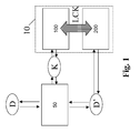
- a non-volatile memory device according to a first embodiment of the invention is schematically illustrated.
- external data D is provided via an input (not shown) to an encryption circuit 50.
- the non-volatile memory device comprises a first non-volatile memory block 100 and a second non-volatile memory block 200, the first non-volatile memory block 100 and the second non-volatile memory block 200 being of a different type such that the they require incompatible external attack techniques in order to retrieve data there from.
- the encryption circuit 50 encrypts the external data D using unique data K from the first non-volatile memory block 100, forming encrypted data D'.
- the encrypted data D' is stored in the second non-volatile memory block 200.
- the first non-volatile memory block 100 and the second non-volatile memory block 200 are located on the same die 10, which is an essential feature of the invention. Together with the fact that the required external attack techniques for both non-volatile memory blocks 100, 200 are incompatible, this feature provides a so-called interlock LCK between both non-volatile memory blocks 100, 200. It is therefore very difficult to retrieve data from both the first non-volatile memory block 100 and the second-non-volatile memory block 200 at the same time.
- the encryption circuit 50 comprises XOR-gates, wherein each bit of the external data D is XOR-ed with a corresponding bit of the unique encryption key K from the first non-volatile memory block 100.
- each bit of the external data D is XOR-ed with a corresponding bit of the unique encryption key K from the first non-volatile memory block 100.
- Fig. 2 the non-volatile memory device according to a second embodiment of the invention is schematically illustrated.
- This embodiment of the non-volatile memory device according to the invention differs from the first embodiment in that the interlock LCK is also provided for the encryption circuit 50.
- the encryption circuit 50 has been provided on the same die 10 as the first non-volatile memory block 100 and the second non-volatile memory block 200.
- Such a measure increases the level of security of the data D.
- External attack of the encryption circuit 50 may also destroy data from the first non-volatile memory block 100 and the second non-volatile memory block 200.
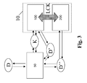
- Fig. 3 the non-volatile memory device according to a third embodiment of the invention is schematically illustrated.
- This embodiment of the non-volatile memory device according to the invention differs from the first embodiment in that a first part of the encrypted data D' is stored into the first non-volatile memory block 100 and a second part of the encrypted data D" is stored into the second non-volatile memory block 200.
- Spreading the encrypted data over the first and second non-volatile memory blocks 100, 200 provides a stronger interlock LCK and thus an additional security.
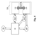
- Fig. 4 the non-volatile memory device according to a fourth embodiment of the invention is schematically illustrated.
- This embodiment of the non-volatile memory device according to the invention differs from the first embodiment in that the encryption key K used by the encryption circuit 50 comprises a first part K1 which has been stored in the first non-volatile memory block 100 and a second part K2 which has been stored in the second non-volatile memory block 200.
- Fig. 5 the non-volatile memory device according to a fifth embodiment of the invention is schematically illustrated.
- This embodiment of the non-volatile memory device according to the invention differs from the earlier mentioned embodiments in that multiple encryption keys K1, K2 are used for encrypting the external data D.
- the multiple encryption keys K1, K2 can be stored on the first non-volatile memory block.
- the encryption circuit 50 uses at least two encryption keys, a first encryption key K1 being stored in the first non-volatile memory block 100 and another encryption key K2 being stored in the second non-volatile memory block 200.
- each external data word to be stored is encrypted using a different encryption key, all encryption keys being stored on the first non-volatile memory block 100.
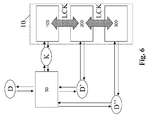
- Fig. 6 the non-volatile memory device according to a sixth embodiment of the invention is schematically illustrated.
- This embodiment of the non-volatile memory device according to the invention differs from the third embodiment in that the non-volatile memory device further comprises a third non-volatile memory block 300.
- the encrypted data D now comprises a first part D' which is being stored on the second non-volatile memory block 200 and a second part D" which is being stored on the third non-volatile memory block 300.
- Spreading the encrypted data over multiple non-volatile memory blocks 200, 300 provides a stronger interlock LCK and thus an additional security.
- the second embodiment dealing with the encryption circuit 50 being provided on the same die as the memory blocks can be easily combined with any one of the other embodiments.
- a word may comprise 16, 32, 64, 128 bits in some examples. However, in principle, in all embodiments, a word can be of any length.
- the encryption circuit 50 in all described embodiments of the non-volatile memory may also be designed to decrypt the encrypted (stored) data D' when reading from the non-volatile memory device.
- a separate decryption circuit (not shown) may be provided.
- this decryption circuit the same interlock aspects hold as for the encryption circuit 50.
- the external data may be encrypted data as well. This measure counteracts attack techniques like IC pin probing when the non-volatile memory device is placed in its application. In such a case the stored encrypted data D' has been encrypted twice.
- the product concerns a single chip secure "product X" manufactured in a 90nm technology.
- the technology features salicided polyfuses to be used as non-volatile memory.
- this memory type is used for the first non-volatile memory block 100.
- the technology also features floating-gate memory as non-volatile memory.
- this memory type is used for the second non-volatile memory block.
- the physical layer of the floating gates in the second non-volatile memory block 200 have been manufactured in the same physical layer as the salicided polyfuses in the first non-volatile memory block 100. This ensures a firm interlock LCK between the first and second non-volatile memories.
- the first non-volatile memory block 100 contains a DieID code, which then forms a hardware private key.
- Product X could further comprise a provider ID, which may be from companies like UPC or KPN. The provider ID can be stored on the first memory block 100 as well, and then forms together with the DieID code the hardware private key.
- the second non-volatile memory block 200 contains the encrypted (using the hardware private key) customer ID (being the original external data).
- the second non-volatile memory block 200 may also comprise an encrypted (using the hardware private key) public key. Sometimes this public key is temporary.
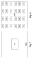
- FIG. 7 illustrates a first non-volatile memory block 100 and a second non-volatile memory block 200, wherein the first non-volatile memory block 100 has been laid out inside the second non-volatile memory block 200.
- Fig. 8 illustrates another approach wherein memory cells 100' of the first non-volatile memory block 100 have been scattered or distributed over the layout of the second non-volatile memory block 200.
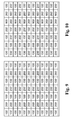
- FIG 9 illustrates a third approach wherein memory cells 100' of the first non-volatile memory block 100 and memory cells 200' of the second non-volatile memory block 200 have been arranged in columns in an alternating way. Such an approach is interesting when the memory blocks 100, 200 are of comparable size.
- Fig 10 illustrates a fourth approach wherein memory cells 100' of the first non-volatile memory block 100 and memory cells 200' of the second non-volatile memory block 200 have been arranged in an alternating way in both the column as well as the row direction. This approach is expected to provide the best interlock. However, for such an approach is most effective in case memory cells 100', 200' of the first 100 and second non-volatile memory blocks 200 are of comparable size.
- Bitline scrambling is a kind of local "encryption" such that a logical bit and a physical bit are scrambled.
- One example is to make use of the multi-layered wiring in the technology through a "spaghetti-like" way so that the bit-line address for every byte (or word) columns are totally different from other bytes/words. In this way, the logic bits are scrambled physically and become very difficult to trace.
- bit-line scrambling makes reverse engineering by means of optical inspection very difficult. Bit-line scrambling can be combined with memory interlacing.
- the invention thus provides a non-volatile memory device, which is more secure against external attack techniques.
- An important aspect of the invention lies in the interlocking of two or more memory blocks combined with the encryption of data being stored thereon.
- the person skilled in the art knows the non-volatile memory technology used in the embodiments.
- the person skilled in the art also knows about non-volatile memory operation and integration. It is the insight of the inventors that a clever combination and integration of more than one memory on a single die combined with the encryption of the data thereon, wherein the encryption key is stored at least on one of the memories, provides a good interlock of the data and therefore a good security against external attacks.
- the invention may be used in various applications like: identification applications, home applications, mobile applications, and set-top boxes (pay TV, satellite TV, etc).
- the invention also provides a method of protecting data in a non-volatile memory device, the method comprising steps of:
Landscapes
- Engineering & Computer Science (AREA)
- Computer Security & Cryptography (AREA)
- Theoretical Computer Science (AREA)
- Computer Hardware Design (AREA)
- Physics & Mathematics (AREA)
- General Engineering & Computer Science (AREA)
- General Physics & Mathematics (AREA)
- Software Systems (AREA)
- Mathematical Physics (AREA)
- Storage Device Security (AREA)
- Read Only Memory (AREA)
- Non-Volatile Memory (AREA)
Priority Applications (8)
| Application Number | Priority Date | Filing Date | Title |
|---|---|---|---|
| EP06121561A EP1906412A1 (fr) | 2006-09-29 | 2006-09-29 | Dispositif de mémoire protégé et méthode de protection de données dans celui-ci |
| AT07826558T ATE462187T1 (de) | 2006-09-29 | 2007-09-27 | Sichere vorrichtung für nicht flüchtige speicher und verfahren zum schutz der darin enthaltenen daten |
| EP07826558A EP2074628B1 (fr) | 2006-09-29 | 2007-09-27 | Dispositif de mémoire protégé et méthode de protéger les données dans le même |
| PCT/IB2007/053922 WO2008038242A2 (fr) | 2006-09-29 | 2007-09-27 | Mémoire rémanente sécurisée et procédé de protection des données stockées dans cette mémoire |
| CN200780035692.1A CN101517654B (zh) | 2006-09-29 | 2007-09-27 | 安全的非易失性存储器装置以及对其中的数据进行保护的方法 |
| US12/443,511 US9165663B2 (en) | 2006-09-29 | 2007-09-27 | Secure non-volatile memory device and method of protecting data therein |
| JP2009529833A JP4909416B2 (ja) | 2006-09-29 | 2007-09-27 | セキュアな不揮発性メモリデバイス及び該メモリデバイス内のデータを保護する方法 |
| DE602007005500T DE602007005500D1 (de) | 2006-09-29 | 2007-09-27 | Sichere vorrichtung für nicht flüchtige speicher und verfahren zum schutz der darin enthaltenen daten |
Applications Claiming Priority (1)
| Application Number | Priority Date | Filing Date | Title |
|---|---|---|---|
| EP06121561A EP1906412A1 (fr) | 2006-09-29 | 2006-09-29 | Dispositif de mémoire protégé et méthode de protection de données dans celui-ci |
Publications (1)
| Publication Number | Publication Date |
|---|---|
| EP1906412A1 true EP1906412A1 (fr) | 2008-04-02 |
Family
ID=37762250
Family Applications (2)
| Application Number | Title | Priority Date | Filing Date |
|---|---|---|---|
| EP06121561A Ceased EP1906412A1 (fr) | 2006-09-29 | 2006-09-29 | Dispositif de mémoire protégé et méthode de protection de données dans celui-ci |
| EP07826558A Active EP2074628B1 (fr) | 2006-09-29 | 2007-09-27 | Dispositif de mémoire protégé et méthode de protéger les données dans le même |
Family Applications After (1)
| Application Number | Title | Priority Date | Filing Date |
|---|---|---|---|
| EP07826558A Active EP2074628B1 (fr) | 2006-09-29 | 2007-09-27 | Dispositif de mémoire protégé et méthode de protéger les données dans le même |
Country Status (7)
| Country | Link |
|---|---|
| US (1) | US9165663B2 (fr) |
| EP (2) | EP1906412A1 (fr) |
| JP (1) | JP4909416B2 (fr) |
| CN (1) | CN101517654B (fr) |
| AT (1) | ATE462187T1 (fr) |
| DE (1) | DE602007005500D1 (fr) |
| WO (1) | WO2008038242A2 (fr) |
Families Citing this family (13)
| Publication number | Priority date | Publication date | Assignee | Title |
|---|---|---|---|---|
| US8028122B2 (en) * | 2008-01-07 | 2011-09-27 | Sandisk Il Ltd. | Methods and systems for classifying storage systems using fixed static-IP addresses |
| US8555089B2 (en) * | 2009-01-08 | 2013-10-08 | Panasonic Corporation | Program execution apparatus, control method, control program, and integrated circuit |
| CN101905578B (zh) * | 2010-07-19 | 2012-07-11 | 山东新北洋信息技术股份有限公司 | 打印机及其控制方法 |
| JP4881468B1 (ja) * | 2010-09-17 | 2012-02-22 | 株式会社東芝 | 記憶装置、保護方法及び電子機器 |
| US9042551B2 (en) | 2012-06-04 | 2015-05-26 | International Business Machines Corporation | Electronically programmable fuse security encryption |
| CN103873227A (zh) * | 2012-12-13 | 2014-06-18 | 艺伦半导体技术股份有限公司 | 一种fpga加密数据流的解密电路及解密方法 |
| WO2014132572A1 (fr) * | 2013-02-28 | 2014-09-04 | パナソニック株式会社 | Dispositif d'enregistrement et de chiffrement, système d'enregistrement et de chiffrement, et procédé d'enregistrement et de chiffrement |
| US9208105B2 (en) * | 2013-05-30 | 2015-12-08 | Dell Products, Lp | System and method for intercept of UEFI block I/O protocol services for BIOS based hard drive encryption support |
| EP3224759B8 (fr) | 2014-11-26 | 2019-06-19 | Hewlett-Packard Development Company, L.P. | Prévention contre les attaques en mémoire |
| US9519533B2 (en) * | 2015-01-28 | 2016-12-13 | Qualcomm Incorporated | Data flow tracking via memory monitoring |
| CN108632655A (zh) * | 2017-03-25 | 2018-10-09 | 张祖豪 | 一种防视疲劳电视 |
| US10491576B1 (en) * | 2017-06-16 | 2019-11-26 | Intuit Inc. | System and method for security breach response using hierarchical cryptographic key management |
| KR20220020636A (ko) * | 2020-08-12 | 2022-02-21 | 삼성전자주식회사 | 메모리 컨트롤러, 상기 메모리 컨트롤러를 포함하는 메모리 장치 및 상기 메모리 컨트롤러의 동작 방법 |
Citations (4)
| Publication number | Priority date | Publication date | Assignee | Title |
|---|---|---|---|---|
| GB2276254A (en) * | 1993-03-20 | 1994-09-21 | Motorola Inc | Protecting data storage devices |
| FR2760871A1 (fr) * | 1997-03-13 | 1998-09-18 | Bull Cp8 | Procede de stockage et d'exploitation d'une information sensible dans un module de securite, et module de securite associe |
| US20030161184A1 (en) * | 2002-02-25 | 2003-08-28 | Aplus Flash Technology, Inc. | Novel highly-integrated flash memory and mask ROM array architecture |
| EP1453060A2 (fr) * | 1999-04-27 | 2004-09-01 | Matsushita Electric Industrial Co., Ltd. | Carte de mémoire semiconducteure et appareil de lecture de donnée |
Family Cites Families (5)
| Publication number | Priority date | Publication date | Assignee | Title |
|---|---|---|---|---|
| US6782101B1 (en) * | 2000-04-20 | 2004-08-24 | The United States Of America As Represented By The Secretary Of The Navy | Encryption using fractal key |
| US6711690B2 (en) * | 2001-09-17 | 2004-03-23 | International Business Machines Corporation | Secure write blocking circuit and method for preventing unauthorized write access to nonvolatile memory |
| US6717222B2 (en) * | 2001-10-07 | 2004-04-06 | Guobiao Zhang | Three-dimensional memory |
| US6906361B2 (en) * | 2002-04-08 | 2005-06-14 | Guobiao Zhang | Peripheral circuits of electrically programmable three-dimensional memory |
| JP2005332221A (ja) * | 2004-05-20 | 2005-12-02 | Renesas Technology Corp | 記憶装置 |
-
2006
- 2006-09-29 EP EP06121561A patent/EP1906412A1/fr not_active Ceased
-
2007
- 2007-09-27 EP EP07826558A patent/EP2074628B1/fr active Active
- 2007-09-27 US US12/443,511 patent/US9165663B2/en active Active
- 2007-09-27 DE DE602007005500T patent/DE602007005500D1/de active Active
- 2007-09-27 JP JP2009529833A patent/JP4909416B2/ja not_active Expired - Fee Related
- 2007-09-27 CN CN200780035692.1A patent/CN101517654B/zh active Active
- 2007-09-27 WO PCT/IB2007/053922 patent/WO2008038242A2/fr not_active Ceased
- 2007-09-27 AT AT07826558T patent/ATE462187T1/de not_active IP Right Cessation
Patent Citations (4)
| Publication number | Priority date | Publication date | Assignee | Title |
|---|---|---|---|---|
| GB2276254A (en) * | 1993-03-20 | 1994-09-21 | Motorola Inc | Protecting data storage devices |
| FR2760871A1 (fr) * | 1997-03-13 | 1998-09-18 | Bull Cp8 | Procede de stockage et d'exploitation d'une information sensible dans un module de securite, et module de securite associe |
| EP1453060A2 (fr) * | 1999-04-27 | 2004-09-01 | Matsushita Electric Industrial Co., Ltd. | Carte de mémoire semiconducteure et appareil de lecture de donnée |
| US20030161184A1 (en) * | 2002-02-25 | 2003-08-28 | Aplus Flash Technology, Inc. | Novel highly-integrated flash memory and mask ROM array architecture |
Also Published As
| Publication number | Publication date |
|---|---|
| CN101517654B (zh) | 2015-02-25 |
| WO2008038242A3 (fr) | 2008-07-17 |
| EP2074628A2 (fr) | 2009-07-01 |
| EP2074628B1 (fr) | 2010-03-24 |
| ATE462187T1 (de) | 2010-04-15 |
| CN101517654A (zh) | 2009-08-26 |
| DE602007005500D1 (de) | 2010-05-06 |
| JP4909416B2 (ja) | 2012-04-04 |
| US20100049906A1 (en) | 2010-02-25 |
| US9165663B2 (en) | 2015-10-20 |
| WO2008038242A2 (fr) | 2008-04-03 |
| JP2010505177A (ja) | 2010-02-18 |
Similar Documents
| Publication | Publication Date | Title |
|---|---|---|
| US9165663B2 (en) | Secure non-volatile memory device and method of protecting data therein | |
| US7907447B2 (en) | Secure non-volatile memory device and method of protecting data therein | |
| CN109495243B (zh) | 使用随机数位的安全系统及安全系统的操作方法 | |
| Skorobogatov | How microprobing can attack encrypted memory | |
| TWI744852B (zh) | 用於快閃記憶體裝置的防駭侵機制 | |
| Helfmeier et al. | Breaking and entering through the silicon | |
| EP2728509B1 (fr) | Dispositif semi-conducteur et procédé d'écriture de la clé de cryptage | |
| TW200845012A (en) | Flash memory device, system and method with randomizing for suppressing error | |
| US20060095975A1 (en) | Semiconductor device | |
| Shamsi et al. | Security of emerging non-volatile memories: Attacks and defenses | |
| CN1102265A (zh) | 数据存储装置 | |
| Xie et al. | A logic resistive memory chip for embedded key storage with physical security | |
| Neve et al. | Memories: A survey of their secure uses in smart cards | |
| JP2007512656A (ja) | セキュリティ行ロック保護された埋込型メモリ | |
| US7003673B1 (en) | Method for storing and operating on data units in a security module and associated security module | |
| US8015416B2 (en) | Memory information protection system and methods | |
| EP1830240A1 (fr) | Systeme de protection d'informations en memoire, memoire a semi-conducteur et procede de protection des informations en memoire | |
| Zonenberg et al. | Extraction of Secrets from 40nm {CMOS} Gate Dielectric Breakdown Antifuses by {FIB} Passive Voltage Contrast | |
| Chavda et al. | Vulnerability analysis of {On-Chip}{Access-Control} memory | |
| Fournier et al. | Memory address scrambling revealed using fault attacks | |
| US20130311790A1 (en) | Secure Three-Dimensional Mask-Programmed Read-Only Memory | |
| Handschuh et al. | Securing flash technology | |
| US20070033380A1 (en) | Method and device for securing an integrated circuit, in particular a microprocessor card | |
| Skorobogatov | Is Hardware Security prepared for unexpected discoveries? | |
| Dyka et al. | Side channel attacks and the non volatile memory of the future |
Legal Events
| Date | Code | Title | Description |
|---|---|---|---|
| PUAI | Public reference made under article 153(3) epc to a published international application that has entered the european phase |
Free format text: ORIGINAL CODE: 0009012 |
|
| AK | Designated contracting states |
Kind code of ref document: A1 Designated state(s): AT BE BG CH CY CZ DE DK EE ES FI FR GB GR HU IE IS IT LI LT LU LV MC NL PL PT RO SE SI SK TR |
|
| AX | Request for extension of the european patent |
Extension state: AL BA HR MK YU |
|
| STAA | Information on the status of an ep patent application or granted ep patent |
Free format text: STATUS: THE APPLICATION HAS BEEN REFUSED |
|
| 18R | Application refused |
Effective date: 20080419 |