EP1906534B1 - Procédé pour déterminer un seuil de commutation et circuit associé. - Google Patents
Procédé pour déterminer un seuil de commutation et circuit associé. Download PDFInfo
- Publication number
- EP1906534B1 EP1906534B1 EP06405407A EP06405407A EP1906534B1 EP 1906534 B1 EP1906534 B1 EP 1906534B1 EP 06405407 A EP06405407 A EP 06405407A EP 06405407 A EP06405407 A EP 06405407A EP 1906534 B1 EP1906534 B1 EP 1906534B1
- Authority
- EP
- European Patent Office
- Prior art keywords
- input
- voltage level
- switch
- circuit arrangement
- voltage signal
- Prior art date
- Legal status (The legal status is an assumption and is not a legal conclusion. Google has not performed a legal analysis and makes no representation as to the accuracy of the status listed.)
- Not-in-force
Links
- 238000000034 method Methods 0.000 title claims abstract description 17
- 238000011161 development Methods 0.000 description 4
- 230000018109 developmental process Effects 0.000 description 4
- 230000005540 biological transmission Effects 0.000 description 3
- 230000000875 corresponding effect Effects 0.000 description 3
- 238000010586 diagram Methods 0.000 description 3
- 230000008569 process Effects 0.000 description 3
- 230000008859 change Effects 0.000 description 2
- 230000001419 dependent effect Effects 0.000 description 2
- 230000007704 transition Effects 0.000 description 2
- 230000008901 benefit Effects 0.000 description 1
- 238000006243 chemical reaction Methods 0.000 description 1
- 230000002596 correlated effect Effects 0.000 description 1
- 230000000694 effects Effects 0.000 description 1
- 210000003608 fece Anatomy 0.000 description 1
- 230000005669 field effect Effects 0.000 description 1
- 238000001914 filtration Methods 0.000 description 1
- 230000036039 immunity Effects 0.000 description 1
- 230000004044 response Effects 0.000 description 1
- 230000035945 sensitivity Effects 0.000 description 1
Images
Classifications
-
- G—PHYSICS
- G05—CONTROLLING; REGULATING
- G05F—SYSTEMS FOR REGULATING ELECTRIC OR MAGNETIC VARIABLES
- G05F1/00—Automatic systems in which deviations of an electric quantity from one or more predetermined values are detected at the output of the system and fed back to a device within the system to restore the detected quantity to its predetermined value or values, i.e. retroactive systems
-
- H—ELECTRICITY
- H03—ELECTRONIC CIRCUITRY
- H03K—PULSE TECHNIQUE
- H03K3/00—Circuits for generating electric pulses; Monostable, bistable or multistable circuits
- H03K3/02—Generators characterised by the type of circuit or by the means used for producing pulses
- H03K3/023—Generators characterised by the type of circuit or by the means used for producing pulses by the use of differential amplifiers or comparators, with internal or external positive feedback
- H03K3/0233—Bistable circuits
- H03K3/02337—Bistables with hysteresis, e.g. Schmitt trigger
-
- H—ELECTRICITY
- H03—ELECTRONIC CIRCUITRY
- H03K—PULSE TECHNIQUE
- H03K5/00—Manipulating of pulses not covered by one of the other main groups of this subclass
- H03K5/01—Shaping pulses
- H03K5/08—Shaping pulses by limiting; by thresholding; by slicing, i.e. combined limiting and thresholding
- H03K5/082—Shaping pulses by limiting; by thresholding; by slicing, i.e. combined limiting and thresholding with an adaptive threshold
- H03K5/084—Shaping pulses by limiting; by thresholding; by slicing, i.e. combined limiting and thresholding with an adaptive threshold modified by switching, e.g. by a periodic signal or by a signal in synchronism with the transitions of the output signal
-
- H—ELECTRICITY
- H03—ELECTRONIC CIRCUITRY
- H03K—PULSE TECHNIQUE
- H03K17/00—Electronic switching or gating, i.e. not by contact-making and –breaking
- H03K17/51—Electronic switching or gating, i.e. not by contact-making and –breaking characterised by the components used
- H03K17/56—Electronic switching or gating, i.e. not by contact-making and –breaking characterised by the components used by the use, as active elements, of semiconductor devices
- H03K17/687—Electronic switching or gating, i.e. not by contact-making and –breaking characterised by the components used by the use, as active elements, of semiconductor devices the devices being field-effect transistors
- H03K17/689—Electronic switching or gating, i.e. not by contact-making and –breaking characterised by the components used by the use, as active elements, of semiconductor devices the devices being field-effect transistors with galvanic isolation between the control circuit and the output circuit
- H03K17/691—Electronic switching or gating, i.e. not by contact-making and –breaking characterised by the components used by the use, as active elements, of semiconductor devices the devices being field-effect transistors with galvanic isolation between the control circuit and the output circuit using transformer coupling
-
- H—ELECTRICITY
- H03—ELECTRONIC CIRCUITRY
- H03K—PULSE TECHNIQUE
- H03K17/00—Electronic switching or gating, i.e. not by contact-making and –breaking
- H03K17/51—Electronic switching or gating, i.e. not by contact-making and –breaking characterised by the components used
- H03K17/78—Electronic switching or gating, i.e. not by contact-making and –breaking characterised by the components used using opto-electronic devices, i.e. light-emitting and photoelectric devices electrically- or optically-coupled
-
- H—ELECTRICITY
- H03—ELECTRONIC CIRCUITRY
- H03K—PULSE TECHNIQUE
- H03K2217/00—Indexing scheme related to electronic switching or gating, i.e. not by contact-making or -breaking covered by H03K17/00
- H03K2217/0036—Means reducing energy consumption
Definitions
- the present invention relates generally to electronic circuitry for converting input signals to output signals, and more particularly to electronic circuitry into which a digital input signal is input that switches a digital output signal upon reaching a certain threshold.
- the present invention relates to electronic circuitry for converting an input voltage signal of a first voltage level into an output voltage signal of a second voltage level, an input unit for inputting the input voltage signal at the first voltage level, a threshold comparison unit for comparing the first voltage level of the input signal with a turn-on threshold, and an output unit for Output of the output signal in response to the comparison of the first voltage level of the input voltage signal are provided with the switch-on threshold.
- Electronic circuit arrangements are known for converting an input voltage signal of a first voltage level into an output voltage signal of a second voltage level.
- Such conventional electronic circuit arrangements allow input voltage signals having a wide input voltage range of, for example 80V to 300V, to convert to corresponding output voltage signals. So that the electronic circuit arrangement can process voltage signals of such a broad input voltage range, the input of the electronic circuit arrangement must have a high-impedance input, ie the electronic circuit arrangement must have a high input impedance with respect to the input voltage signal to be processed or amplified.
- US 4,523,143 discloses a switching arrangement for testing signals.
- a level shifter is used to assist in obtaining sufficient voltage at the output of the circuit.
- An input impedance is switched manually and based on the level of the signal being tested.
- US 2002/0083352 discloses a level shifter each including a low power consumption and wide range shifter, one of which is selected after a short delay and depending on the level of the input signal
- An essential concept of the invention is to switch the input impedance of an electronic circuit arrangement such that a switch-on time can be detected without interference and that at the same time a high power loss is avoided by an excessively high input current.
- An excessively high input current is avoided by switching the input impedance to another time, which is a delay period after the switch-on time.
- Time, d. H. after a reliable and not affected by disturbances switching a high input impedance can be provided in the electronic circuit arrangement, so that after a reliable switching an input current does not rise excessively and thus an increase in power loss can be avoided.
- a trip unit which supplies a switching signal for switching the input impedance of the circuit from a low value to a high value when the first voltage level of the input voltage signal exceeds the switch-on threshold value after a predetermined delay time period of the input impedance switching unit.
- a primary-side circuit device and a secondary side circuit device coupled via a coupler.
- the primary-side circuit device in this case contains the input impedance switching unit for switching the input impedance of the circuit arrangement.
- the coupler is designed as a magnetic coupler. More preferably, the coupler is designed as an optocoupler.
- the threshold value comparison unit has a circuit hysteresis such that a switch-off threshold value is below a switch-on threshold value in terms of voltage.
- the input impedance of the circuit arrangement has a low value as long as the first voltage level of the input voltage signal is less than the switch-on threshold.
- the input impedance of the circuitry is high when the first voltage level of the input voltage signal exceeds the turn-on threshold.
- the input impedance switching unit switches the input impedance of the circuit arrangement from a low value to a high value at a turn-on timing when the first voltage level of the input voltage signal exceeds the turn-on threshold.
- the input impedance of the circuit is switched from a high value to a low value at a switching time, after an elapse of a delay period after the power-on time when the first voltage level of the input voltage signal has exceeded the switch-on threshold.
- the output signal is switched at the switching timing after an elapse of a delay time period after the turn-on timing when the first voltage level of the input voltage signal has exceeded the turn-on threshold.
- an input current to the circuit during the delay period, from the turn-on time to the changeover time assumes a higher current value than after the changeover time.
- the electronic circuit arrangement according to the invention for converting an input voltage signal into an output signal and the corresponding conversion method makes it possible to determine a switch-on time precisely without the influence of interference, wherein an increase in power loss is avoided.
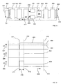
- Fig. 1 shows a schematic block diagram of an electronic circuit arrangement for converting an input voltage signal into an output signal according to a preferred embodiment of the present invention.
- a primary-side circuit device 100 is connected to a secondary-side circuit device 200 via a coupler 300.
- the coupler 300 may be implemented as an optocoupler or as a GMR coupler (Giant Magnetic Resistance).
- An input voltage signal 401 to be processed is applied to the primary-side circuit device 100, which leads to an input current 403 in the circuit arrangement.
- an input unit 101 is used for inputting the input voltage signal 401 and the input current 403, for inputting the input voltage signal 401 and the input current 403, an input unit 101 is used.
- the input signals are first supplied to a primary-side filter unit 102, in which gross disturbances of the input voltage signal are filtered out.
- An essential element of the electronic circuit arrangement according to the invention is an input impedance switching unit designated by reference numeral 103.
- the input impedance switching unit is supplied with a switching signal 417 from a trip unit 106 to be described below.
- the input impedance switching unit 103 switches over the input impedance of the electronic circuit arrangement, ie one Input impedance, which is seen when inputting an input voltage signal 401 and an input current 403 into the input unit 101, from a low input impedance value to a high input impedance value, and vice versa.
- a low input impedance value is required when a level change of an input voltage signal with the least possible influence of external noise is to be detected, while a high value of input impedance is required when the input current flowing into the circuit 403 is to be limited and so that excessive power dissipation should be avoided.
- a threshold comparison unit 104 Downstream of the input impedance switching unit 103 is a threshold comparison unit 104. As described below with reference to FIG Fig. 2 (a) will be explained in the threshold comparison unit 104, a comparison of the input voltage signal 401 both with a switch-404 at turn on the output signal 402 and a Ausschaltschwellwert 405 when turning off the output signal 402th
- a current source 105 connected downstream of the threshold comparison unit 104 which supplies a current as a transmission signal 416 to the coupler device 300. Furthermore, the threshold comparison unit 104 is followed by the tripping unit 106, which is addressed by the threshold value comparison unit 104 via a tripping unit control signal 415.
- the switch-on operations, switching operations and switch-off processes as well as the corresponding delay times are described below FIGS. 2 (a), 2 (b) and 2 (c) explained.
- secondary-side circuit device 200 has a secondary-side filter unit 201 for filtering the output from the coupler 300 electrical Signal and a control unit 202 on.
- the control unit 202 processes the signal obtained via the coupler 200 from the primary-side circuit device 100 and outputs via an output unit 203 an output signal 402, which is described below in FIG Fig. 2 (b) is illustrated.
- FIG. 3 illustrates a timing diagram in total, wherein waveforms over a time 406 of an input voltage value 407, an output voltage value 408 and an input current value 409 are shown correlated with one another over time.
- Fig. 2 (a) shows the input voltage value 407 as a function of time 406, where in Fig. 2 (a) at the same time the above-mentioned turn-on and turn-off thresholds 404 and 405 are plotted (dashed horizontal lines).
- a transition of the input voltage signal from a zero level to a first voltage level occurs.
- This transition from a zero level to the first voltage level in the input voltage signal 401 is intended to cause the output signal 402 (see FIG Fig. 2 (b) ) also rises from a zero level to a second voltage level. Like in the Fig. 2 As can be seen, however, such an increase takes place only after a delay time period 410 which can be set in the threshold value comparison unit 104.
- the delay time duration 410 is the time interval between a switching time 412 and the turn-on time 411.
- the trip unit 106 provides feedback to the threshold comparison unit 104 such that it is supplied with the switch signal 417.
- the threshold comparison unit 104 controls, via the current source control signal, the current source 105, which results in a transmission signal 416 being transmitted by the coupler 300, which then leads on the secondary side to an increase, from a zero level to the second voltage level, of the output signal 402 ,
- the output signal 402 follows the voltage profile of the input voltage signal 401 only after a delay period 410 after the switch-on time 411.
- the essential advantage of such a switching method is that, during the delay time period 410, faults which are applied, for example, to the input unit 101 of the electronic circuit arrangement have no influence on the switchover time.
- This high input current 403 is lowered to a low current (typically 1 mA) at the switchover time 412, so the power loss of the circuit arrangement can not exceed a permissible maximum value.
- a turn-off time 413 which represents the turning off of the input voltage signal 401 from the first voltage level to the zero level.
- the input impedance of the electronic circuitry assumes a high value since it has already switched from a high input impedance value to a low input impedance value at the switchover time 412.
- this is irrelevant with regard to the input disturbances since, when the input voltage signal 401 is switched off, a low-impedance termination of the input unit 101 is provided anyway.
- the input impedance switching unit includes field effect transistors (FET) which become conductive at a control current.
- FET field effect transistors
- the peak current value of the input current 403 during the delay time period 410 may be several amperes while the current value of the remaining input current path 403 is only a few milliamps (mA).
Landscapes
- Physics & Mathematics (AREA)
- Nonlinear Science (AREA)
- Engineering & Computer Science (AREA)
- Automation & Control Theory (AREA)
- General Physics & Mathematics (AREA)
- Radar, Positioning & Navigation (AREA)
- Electromagnetism (AREA)
- Electronic Switches (AREA)
- Manipulation Of Pulses (AREA)
- Logic Circuits (AREA)
- Networks Using Active Elements (AREA)
- Analogue/Digital Conversion (AREA)
- Testing Of Individual Semiconductor Devices (AREA)
- Processing Of Color Television Signals (AREA)
Claims (13)
- Arrangement de circuit électronique pour convertir un signal de tension d'entrée (401) d'un premier niveau de tension en un signal de sortie (402) d'un deuxième niveau de tension, comprenant :a) une unité d'entrée (101) pour l'entrée du signal de tension d'entrée (401) au premier niveau de tension ;b) une unité de comparaison de valeur de seuil (104) pour comparer le premier niveau de tension du signal de tension d'entrée (401) avec une valeur de seuil de mise en marche (404) ; etc) une unité de délivrance (203) pour délivrer le signal de sortie (402) en fonction de la comparaison du premier niveau de tension du signal de tension d'entrée (401) avec la valeur de seuil de mise en marche (404),
caractérisé en ce
que l'arrangement de circuit présente en outre : d) une unité de permutation d'impédance d'entrée (103) pour permuter une impédance d'entrée de l'arrangement de circuit d'une valeur faible à une valeur élevée après un temps de retard prédéfini (410) après un instant (411) auquel le premier niveau de tension du signal de tension d'entrée (401) a dépassé la valeur de seuil de mise en marche (404). - Arrangement de circuit selon la revendication 1, caractérisé en ce qu'il existe une unité de déclenchement (106) qui achemine à l'unité de permutation d'impédance d'entrée (103) un signal de permutation (417) pour permuter l'impédance d'entrée de l'arrangement de circuit d'une valeur faible à une valeur élevée après temps de retard prédéfini (410).
- Arrangement de circuit selon la revendication 1, caractérisé en ce qu'il existe un dispositif de commutation côté primaire (100) et un dispositif de commutation côté secondaire (200), lesquels sont accouplés par le biais d'un dispositif de couplage (300).
- Arrangement de circuit selon la revendication 3, caractérisé en ce que le dispositif de couplage (300) est réalisé sous la forme d'un optocoupleur.
- Arrangement de circuit selon la revendication 3, caractérisé en ce que le dispositif de couplage (300) est réalisé sous la forme d'un coupleur magnétique.
- Arrangement de circuit selon la revendication 1, caractérisé en ce que l'unité de comparaison de valeur de seuil (104) présente une hystérésis de comparaison.
- Procédé de conversion d'un signal de tension d'entrée (401) d'un premier niveau de tension en un signal de sortie (402) d'un deuxième niveau de tension, comprenant les étapes suivantes :a) entrée du signal de tension d'entrée (401) au premier niveau de tension au moyen d'une unité d'entrée (101) ;b) comparaison du premier niveau de tension du signal de tension d'entrée (401) avec une valeur de seuil de mise en marche (404) au moyen d'une unité de comparaison de valeur de seuil (104) ; etc) délivrance du signal de sortie (402) en fonction de la comparaison du premier niveau de tension du signal de tension d'entrée (401) avec la valeur de seuil de mise en marche (404) au moyen d'une unité de délivrance (203),caractérisé en ce
que le procédé présente les étapes suivantes :d) permutation d'une impédance d'entrée de l'arrangement de circuit d'une valeur faible à une valeur élevée après un temps de retard prédéfini (410) après un instant (411) auquel le premier niveau de tension du signal de tension d'entrée (401) a dépassé la valeur de seuil de mise en marche (404). - Procédé selon la revendication 7, caractérisé en ce que l'impédance d'entrée de l'arrangement de circuit présente une valeur faible tant que le premier niveau de tension du signal de tension d'entrée (401) est inférieur à la valeur de seuil de mise en marche.
- Procédé selon la revendication 7, caractérisé en ce que l'impédance d'entrée de l'arrangement de circuit présente une valeur élevée lorsque le premier niveau de tension du signal de tension d'entrée (401) dépasse la valeur de seuil de mise en marche.
- Procédé selon la revendication 7, caractérisé en ce que l'unité de permutation d'impédance d'entrée (103) permute l'impédance d'entrée de l'arrangement de circuit d'une valeur faible à une valeur élevée à un instant de permutation (412) lorsque le premier niveau de tension du signal de tension d'entrée (401) a dépassé la valeur de seuil de mise en marche (404).
- Procédé selon la revendication 7, caractérisé en ce que l'impédance d'entrée de l'arrangement de circuit est permutée d'une valeur élevée à une valeur faible à un instant de permutation (412) après l'écoulement d'un temps de retard (410) après l'instant de mise en marche (411), lorsque le premier niveau de tension du signal de tension d'entrée (401) a dépassé la valeur de seuil de mise en marche (404).
- Procédé selon la revendication 7, caractérisé en ce que le signal de sortie (402) est permuté à l'instant de permutation (412), après l'écoulement d'un temps de retard (410) après l'instant de mise en marche (411), auquel le premier niveau de tension du signal de tension d'entrée (401) dépasse la valeur de seuil de mise en marche (404).
- Procédé selon la revendication 7, caractérisé en ce qu'un courant d'entrée (403) dans l'arrangement de circuit prend une valeur de courant plus élevée pendant le temps de retard (410) entre l'instant de mise en marche (411) et l'instant de permutation (412) qu'après l'instant de permutation (412).
Priority Applications (7)
| Application Number | Priority Date | Filing Date | Title |
|---|---|---|---|
| EP06405407A EP1906534B1 (fr) | 2006-09-28 | 2006-09-28 | Procédé pour déterminer un seuil de commutation et circuit associé. |
| DE502006008720T DE502006008720D1 (de) | 2006-09-28 | 2006-09-28 | Verfahren zum Bestimmen einer Einschaltschwelle und elektronische Schaltungsanordnung zur Durchführung des Verfahrens |
| AT06405407T ATE495580T1 (de) | 2006-09-28 | 2006-09-28 | Verfahren zum bestimmen einer einschaltschwelle und elektronische schaltungsanordnung zur durchführung des verfahrens |
| KR1020070095302A KR101433818B1 (ko) | 2006-09-28 | 2007-09-19 | 스위치-온 임계치를 결정하기 위한 방법과 이 방법을수행하기 위한 전자 회로 장치 |
| US11/902,348 US7663421B2 (en) | 2006-09-28 | 2007-09-20 | Method for determining a switch-on threshold and electronic circuit arrangement for carrying out the method |
| CN2007101613328A CN101154943B (zh) | 2006-09-28 | 2007-09-28 | 确定接通阈的方法和执行该方法的电子电路装置 |
| JP2007254287A JP2008086022A (ja) | 2006-09-28 | 2007-09-28 | スイッチオン閾値を決定するための方法およびこの方法を実行するための電子回路配置 |
Applications Claiming Priority (1)
| Application Number | Priority Date | Filing Date | Title |
|---|---|---|---|
| EP06405407A EP1906534B1 (fr) | 2006-09-28 | 2006-09-28 | Procédé pour déterminer un seuil de commutation et circuit associé. |
Publications (2)
| Publication Number | Publication Date |
|---|---|
| EP1906534A1 EP1906534A1 (fr) | 2008-04-02 |
| EP1906534B1 true EP1906534B1 (fr) | 2011-01-12 |
Family
ID=37771114
Family Applications (1)
| Application Number | Title | Priority Date | Filing Date |
|---|---|---|---|
| EP06405407A Not-in-force EP1906534B1 (fr) | 2006-09-28 | 2006-09-28 | Procédé pour déterminer un seuil de commutation et circuit associé. |
Country Status (7)
| Country | Link |
|---|---|
| US (1) | US7663421B2 (fr) |
| EP (1) | EP1906534B1 (fr) |
| JP (1) | JP2008086022A (fr) |
| KR (1) | KR101433818B1 (fr) |
| CN (1) | CN101154943B (fr) |
| AT (1) | ATE495580T1 (fr) |
| DE (1) | DE502006008720D1 (fr) |
Families Citing this family (6)
| Publication number | Priority date | Publication date | Assignee | Title |
|---|---|---|---|---|
| KR101503227B1 (ko) | 2007-04-11 | 2015-03-16 | 레드.컴 인코포레이티드 | 비디오 카메라 |
| US20200005434A1 (en) * | 2007-04-11 | 2020-01-02 | Red.Com, Llc | Video capture devices and methods |
| US8237830B2 (en) | 2007-04-11 | 2012-08-07 | Red.Com, Inc. | Video camera |
| CA2812119C (fr) * | 2010-09-16 | 2015-11-24 | Abb Technology Ag | Entree logique a impedance variable |
| JP2016508700A (ja) | 2013-02-14 | 2016-03-22 | レッド.コム,インコーポレイテッド | ビデオカメラ |
| WO2019010233A1 (fr) | 2017-07-05 | 2019-01-10 | Red. Com, Llc | Traitement de données d'image vidéo dans des dispositifs électroniques |
Family Cites Families (8)
| Publication number | Priority date | Publication date | Assignee | Title |
|---|---|---|---|---|
| US4523143A (en) * | 1982-06-18 | 1985-06-11 | Fairchild Camera And Instrument Corporation | Digital logic level comparator particularly for digital test systems |
| US5182716A (en) * | 1990-06-15 | 1993-01-26 | Allen-Bradley Company, Inc. | Injection molding controller with controlled variable learning |
| US6211719B1 (en) * | 1999-04-19 | 2001-04-03 | Globespan Semiconductor Inc. | Power control circuit for a line driver |
| US6420910B1 (en) * | 1999-04-27 | 2002-07-16 | International Business Machines Corporation | Quasi-current sensing input impedance controlled preamplifier for magnetoresistive elements |
| US6351172B1 (en) * | 2000-02-29 | 2002-02-26 | Dmel Inc. | High-speed output driver with an impedance adjustment scheme |
| JP3532153B2 (ja) * | 2000-12-22 | 2004-05-31 | 沖電気工業株式会社 | レベルシフタ制御回路 |
| JP4026593B2 (ja) * | 2003-12-25 | 2007-12-26 | セイコーエプソン株式会社 | 受信装置 |
| US7307458B1 (en) * | 2005-05-27 | 2007-12-11 | National Semiconductor Corporation | Voltage mode serial interface driver with PVT compensated impedance |
-
2006
- 2006-09-28 DE DE502006008720T patent/DE502006008720D1/de active Active
- 2006-09-28 AT AT06405407T patent/ATE495580T1/de active
- 2006-09-28 EP EP06405407A patent/EP1906534B1/fr not_active Not-in-force
-
2007
- 2007-09-19 KR KR1020070095302A patent/KR101433818B1/ko not_active Expired - Fee Related
- 2007-09-20 US US11/902,348 patent/US7663421B2/en not_active Expired - Fee Related
- 2007-09-28 CN CN2007101613328A patent/CN101154943B/zh not_active Expired - Fee Related
- 2007-09-28 JP JP2007254287A patent/JP2008086022A/ja active Pending
Also Published As
| Publication number | Publication date |
|---|---|
| US20080284485A1 (en) | 2008-11-20 |
| US7663421B2 (en) | 2010-02-16 |
| ATE495580T1 (de) | 2011-01-15 |
| EP1906534A1 (fr) | 2008-04-02 |
| CN101154943A (zh) | 2008-04-02 |
| KR20080029815A (ko) | 2008-04-03 |
| JP2008086022A (ja) | 2008-04-10 |
| KR101433818B1 (ko) | 2014-09-23 |
| DE502006008720D1 (de) | 2011-02-24 |
| CN101154943B (zh) | 2012-07-11 |
Similar Documents
| Publication | Publication Date | Title |
|---|---|---|
| EP2980659B1 (fr) | Dispositif et procédé destinés à la surveillance et la commutation d'un circuit de charge | |
| EP2980660B1 (fr) | Procédé et dispositif de surveillance et de commutation d'un circuit de charge | |
| DE102016112361B4 (de) | Elektrische leistungsumwandlungsvorrichtung | |
| EP1906534B1 (fr) | Procédé pour déterminer un seuil de commutation et circuit associé. | |
| DE102011013529B4 (de) | Leistungsversorgungs-Auswahleinrichtung und Verfahren zum Minimieren eines Einschaltstroms in einer Leistungsversorgungs-Auswahleinrichtung und Leistungsversorgungs-Auswahlsystem | |
| DE102005023652B3 (de) | Schaltungsanordnung mit Fehlererkennung zur Ansteuerung von Leistungshalbleiterschaltern und zugehöriges Verfahren | |
| WO2024175243A1 (fr) | Dispositif et procédé de surveillance d'éléments de commutation à semi-conducteur, module de puissance et convertisseur de puissance électrique | |
| DE112021000078T5 (de) | Kurzschlussbestimmungsvorrichtung, schaltgerät und verfahren zur bestimmung eines kurzschlusses | |
| EP4367698B1 (fr) | Appareil de commutation à tension continue pourvu d'une protection contre les défauts à la terre | |
| DE1588578A1 (de) | Erregungsschaltung fuer einen Elektromagnet | |
| DE102008011603B4 (de) | Schaltung und Verfahren zur Signalspannungsübertragung innerhalb eines Treibers eines Leistungshalbleiterschalters | |
| DE102009045220B4 (de) | System und Verfahren zum Begrenzen von Stromoszillationen | |
| EP3652860B1 (fr) | Convertisseur de niveau et procédé de conversion de valeurs de niveau dans des dispositifs de commande de véhicule | |
| WO2007060165A1 (fr) | Circuiterie et procede pour commander un composant electronique par le biais d'un signal de sortie d'un microprocesseur | |
| EP3709513B1 (fr) | Dispositif de commutation ainsi que procédé de fonctionnement d'un dispositif de commutation | |
| WO2022248389A1 (fr) | Surveillance de courant de défaut à tension continue pour détecter un défaut d'isolation | |
| DE102020205024A1 (de) | Schaltvorrichtung und Verfahren zur Ansteuerung eines Halbleiterschalters | |
| AT523936A4 (de) | Verfahren und vorrichtung zum steuern eines halbleiterschalters | |
| DE19842045B4 (de) | Schutzverfahren für ein steuerbares nicht einrastendes Halbleiter-Schaltelement und hierzu korrespondierende Schutzschaltung | |
| DE69820837T2 (de) | Statischer Endschalter zur Betätigung eines Leistungsschalters | |
| EP1086477B1 (fr) | Circuit d'entree pour signaux de courant alternatif a intensite relativement elevee a surveiller | |
| DE102005005466B4 (de) | Schaltungsanordnung für eine Meldeeinrichtung zur Überwachung von Schaltzuständen zumindest eines Schaltkontaktes | |
| WO1996026577A1 (fr) | Procede et montage permettant de relier une charge a un conducteur | |
| DE3717482C2 (fr) | ||
| DE19526493A1 (de) | Verfahren zur Steuerung eines Laststromkreises |
Legal Events
| Date | Code | Title | Description |
|---|---|---|---|
| PUAI | Public reference made under article 153(3) epc to a published international application that has entered the european phase |
Free format text: ORIGINAL CODE: 0009012 |
|
| AK | Designated contracting states |
Kind code of ref document: A1 Designated state(s): AT BE BG CH CY CZ DE DK EE ES FI FR GB GR HU IE IS IT LI LT LU LV MC NL PL PT RO SE SI SK TR |
|
| AX | Request for extension of the european patent |
Extension state: AL BA HR MK YU |
|
| 17P | Request for examination filed |
Effective date: 20080904 |
|
| AKX | Designation fees paid |
Designated state(s): AT BE BG CH CY CZ DE DK EE ES FI FR GB GR HU IE IS IT LI LT LU LV MC NL PL PT RO SE SI SK TR |
|
| GRAP | Despatch of communication of intention to grant a patent |
Free format text: ORIGINAL CODE: EPIDOSNIGR1 |
|
| GRAS | Grant fee paid |
Free format text: ORIGINAL CODE: EPIDOSNIGR3 |
|
| GRAA | (expected) grant |
Free format text: ORIGINAL CODE: 0009210 |
|
| AK | Designated contracting states |
Kind code of ref document: B1 Designated state(s): AT BE BG CH CY CZ DE DK EE ES FI FR GB GR HU IE IS IT LI LT LU LV MC NL PL PT RO SE SI SK TR |
|
| REG | Reference to a national code |
Ref country code: GB Ref legal event code: FG4D Free format text: NOT ENGLISH |
|
| REG | Reference to a national code |
Ref country code: CH Ref legal event code: EP |
|
| REG | Reference to a national code |
Ref country code: CH Ref legal event code: NV Representative=s name: ABB SCHWEIZ AG INTELLECTUAL PROPERTY (CH-LC/IP) |
|
| REG | Reference to a national code |
Ref country code: IE Ref legal event code: FG4D Free format text: LANGUAGE OF EP DOCUMENT: GERMAN |
|
| REF | Corresponds to: |
Ref document number: 502006008720 Country of ref document: DE Date of ref document: 20110224 Kind code of ref document: P |
|
| REG | Reference to a national code |
Ref country code: DE Ref legal event code: R096 Ref document number: 502006008720 Country of ref document: DE Effective date: 20110224 |
|
| REG | Reference to a national code |
Ref country code: NL Ref legal event code: VDEP Effective date: 20110112 |
|
| LTIE | Lt: invalidation of european patent or patent extension |
Effective date: 20110112 |
|
| PG25 | Lapsed in a contracting state [announced via postgrant information from national office to epo] |
Ref country code: SE Free format text: LAPSE BECAUSE OF FAILURE TO SUBMIT A TRANSLATION OF THE DESCRIPTION OR TO PAY THE FEE WITHIN THE PRESCRIBED TIME-LIMIT Effective date: 20110112 Ref country code: LT Free format text: LAPSE BECAUSE OF FAILURE TO SUBMIT A TRANSLATION OF THE DESCRIPTION OR TO PAY THE FEE WITHIN THE PRESCRIBED TIME-LIMIT Effective date: 20110112 Ref country code: PT Free format text: LAPSE BECAUSE OF FAILURE TO SUBMIT A TRANSLATION OF THE DESCRIPTION OR TO PAY THE FEE WITHIN THE PRESCRIBED TIME-LIMIT Effective date: 20110512 Ref country code: LV Free format text: LAPSE BECAUSE OF FAILURE TO SUBMIT A TRANSLATION OF THE DESCRIPTION OR TO PAY THE FEE WITHIN THE PRESCRIBED TIME-LIMIT Effective date: 20110112 Ref country code: GR Free format text: LAPSE BECAUSE OF FAILURE TO SUBMIT A TRANSLATION OF THE DESCRIPTION OR TO PAY THE FEE WITHIN THE PRESCRIBED TIME-LIMIT Effective date: 20110413 Ref country code: IS Free format text: LAPSE BECAUSE OF FAILURE TO SUBMIT A TRANSLATION OF THE DESCRIPTION OR TO PAY THE FEE WITHIN THE PRESCRIBED TIME-LIMIT Effective date: 20110512 Ref country code: ES Free format text: LAPSE BECAUSE OF FAILURE TO SUBMIT A TRANSLATION OF THE DESCRIPTION OR TO PAY THE FEE WITHIN THE PRESCRIBED TIME-LIMIT Effective date: 20110423 |
|
| REG | Reference to a national code |
Ref country code: IE Ref legal event code: FD4D |
|
| PG25 | Lapsed in a contracting state [announced via postgrant information from national office to epo] |
Ref country code: FI Free format text: LAPSE BECAUSE OF FAILURE TO SUBMIT A TRANSLATION OF THE DESCRIPTION OR TO PAY THE FEE WITHIN THE PRESCRIBED TIME-LIMIT Effective date: 20110112 Ref country code: BG Free format text: LAPSE BECAUSE OF FAILURE TO SUBMIT A TRANSLATION OF THE DESCRIPTION OR TO PAY THE FEE WITHIN THE PRESCRIBED TIME-LIMIT Effective date: 20110412 Ref country code: NL Free format text: LAPSE BECAUSE OF FAILURE TO SUBMIT A TRANSLATION OF THE DESCRIPTION OR TO PAY THE FEE WITHIN THE PRESCRIBED TIME-LIMIT Effective date: 20110112 Ref country code: PL Free format text: LAPSE BECAUSE OF FAILURE TO SUBMIT A TRANSLATION OF THE DESCRIPTION OR TO PAY THE FEE WITHIN THE PRESCRIBED TIME-LIMIT Effective date: 20110112 Ref country code: CY Free format text: LAPSE BECAUSE OF FAILURE TO SUBMIT A TRANSLATION OF THE DESCRIPTION OR TO PAY THE FEE WITHIN THE PRESCRIBED TIME-LIMIT Effective date: 20110112 Ref country code: SI Free format text: LAPSE BECAUSE OF FAILURE TO SUBMIT A TRANSLATION OF THE DESCRIPTION OR TO PAY THE FEE WITHIN THE PRESCRIBED TIME-LIMIT Effective date: 20110112 |
|
| PG25 | Lapsed in a contracting state [announced via postgrant information from national office to epo] |
Ref country code: IE Free format text: LAPSE BECAUSE OF FAILURE TO SUBMIT A TRANSLATION OF THE DESCRIPTION OR TO PAY THE FEE WITHIN THE PRESCRIBED TIME-LIMIT Effective date: 20110112 Ref country code: EE Free format text: LAPSE BECAUSE OF FAILURE TO SUBMIT A TRANSLATION OF THE DESCRIPTION OR TO PAY THE FEE WITHIN THE PRESCRIBED TIME-LIMIT Effective date: 20110112 Ref country code: DK Free format text: LAPSE BECAUSE OF FAILURE TO SUBMIT A TRANSLATION OF THE DESCRIPTION OR TO PAY THE FEE WITHIN THE PRESCRIBED TIME-LIMIT Effective date: 20110112 |
|
| PLBE | No opposition filed within time limit |
Free format text: ORIGINAL CODE: 0009261 |
|
| STAA | Information on the status of an ep patent application or granted ep patent |
Free format text: STATUS: NO OPPOSITION FILED WITHIN TIME LIMIT |
|
| PG25 | Lapsed in a contracting state [announced via postgrant information from national office to epo] |
Ref country code: SK Free format text: LAPSE BECAUSE OF FAILURE TO SUBMIT A TRANSLATION OF THE DESCRIPTION OR TO PAY THE FEE WITHIN THE PRESCRIBED TIME-LIMIT Effective date: 20110112 Ref country code: RO Free format text: LAPSE BECAUSE OF FAILURE TO SUBMIT A TRANSLATION OF THE DESCRIPTION OR TO PAY THE FEE WITHIN THE PRESCRIBED TIME-LIMIT Effective date: 20110112 Ref country code: CZ Free format text: LAPSE BECAUSE OF FAILURE TO SUBMIT A TRANSLATION OF THE DESCRIPTION OR TO PAY THE FEE WITHIN THE PRESCRIBED TIME-LIMIT Effective date: 20110112 |
|
| 26N | No opposition filed |
Effective date: 20111013 |
|
| PG25 | Lapsed in a contracting state [announced via postgrant information from national office to epo] |
Ref country code: IT Free format text: LAPSE BECAUSE OF FAILURE TO SUBMIT A TRANSLATION OF THE DESCRIPTION OR TO PAY THE FEE WITHIN THE PRESCRIBED TIME-LIMIT Effective date: 20110112 |
|
| REG | Reference to a national code |
Ref country code: DE Ref legal event code: R097 Ref document number: 502006008720 Country of ref document: DE Effective date: 20111013 |
|
| BERE | Be: lapsed |
Owner name: ABB TECHNOLOGY A.G. Effective date: 20110930 |
|
| PG25 | Lapsed in a contracting state [announced via postgrant information from national office to epo] |
Ref country code: MC Free format text: LAPSE BECAUSE OF NON-PAYMENT OF DUE FEES Effective date: 20110930 |
|
| GBPC | Gb: european patent ceased through non-payment of renewal fee |
Effective date: 20110928 |
|
| PG25 | Lapsed in a contracting state [announced via postgrant information from national office to epo] |
Ref country code: BE Free format text: LAPSE BECAUSE OF NON-PAYMENT OF DUE FEES Effective date: 20110930 |
|
| PG25 | Lapsed in a contracting state [announced via postgrant information from national office to epo] |
Ref country code: GB Free format text: LAPSE BECAUSE OF NON-PAYMENT OF DUE FEES Effective date: 20110928 |
|
| REG | Reference to a national code |
Ref country code: AT Ref legal event code: MM01 Ref document number: 495580 Country of ref document: AT Kind code of ref document: T Effective date: 20110928 |
|
| PG25 | Lapsed in a contracting state [announced via postgrant information from national office to epo] |
Ref country code: AT Free format text: LAPSE BECAUSE OF NON-PAYMENT OF DUE FEES Effective date: 20110928 |
|
| PG25 | Lapsed in a contracting state [announced via postgrant information from national office to epo] |
Ref country code: LU Free format text: LAPSE BECAUSE OF NON-PAYMENT OF DUE FEES Effective date: 20110928 |
|
| PG25 | Lapsed in a contracting state [announced via postgrant information from national office to epo] |
Ref country code: TR Free format text: LAPSE BECAUSE OF FAILURE TO SUBMIT A TRANSLATION OF THE DESCRIPTION OR TO PAY THE FEE WITHIN THE PRESCRIBED TIME-LIMIT Effective date: 20110112 |
|
| PG25 | Lapsed in a contracting state [announced via postgrant information from national office to epo] |
Ref country code: HU Free format text: LAPSE BECAUSE OF FAILURE TO SUBMIT A TRANSLATION OF THE DESCRIPTION OR TO PAY THE FEE WITHIN THE PRESCRIBED TIME-LIMIT Effective date: 20110112 |
|
| PGFP | Annual fee paid to national office [announced via postgrant information from national office to epo] |
Ref country code: DE Payment date: 20140922 Year of fee payment: 9 Ref country code: CH Payment date: 20140919 Year of fee payment: 9 |
|
| PGFP | Annual fee paid to national office [announced via postgrant information from national office to epo] |
Ref country code: FR Payment date: 20140919 Year of fee payment: 9 |
|
| REG | Reference to a national code |
Ref country code: DE Ref legal event code: R119 Ref document number: 502006008720 Country of ref document: DE |
|
| REG | Reference to a national code |
Ref country code: CH Ref legal event code: PL |
|
| REG | Reference to a national code |
Ref country code: FR Ref legal event code: ST Effective date: 20160531 |
|
| PG25 | Lapsed in a contracting state [announced via postgrant information from national office to epo] |
Ref country code: DE Free format text: LAPSE BECAUSE OF NON-PAYMENT OF DUE FEES Effective date: 20160401 Ref country code: LI Free format text: LAPSE BECAUSE OF NON-PAYMENT OF DUE FEES Effective date: 20150930 Ref country code: CH Free format text: LAPSE BECAUSE OF NON-PAYMENT OF DUE FEES Effective date: 20150930 |
|
| PG25 | Lapsed in a contracting state [announced via postgrant information from national office to epo] |
Ref country code: FR Free format text: LAPSE BECAUSE OF NON-PAYMENT OF DUE FEES Effective date: 20150930 |