EP1909308A1 - Mandrin électrostatique et feuille d électrode pour mandrin électrostatique - Google Patents
Mandrin électrostatique et feuille d électrode pour mandrin électrostatique Download PDFInfo
- Publication number
- EP1909308A1 EP1909308A1 EP06767996A EP06767996A EP1909308A1 EP 1909308 A1 EP1909308 A1 EP 1909308A1 EP 06767996 A EP06767996 A EP 06767996A EP 06767996 A EP06767996 A EP 06767996A EP 1909308 A1 EP1909308 A1 EP 1909308A1
- Authority
- EP
- European Patent Office
- Prior art keywords
- opening portions
- electrostatic chuck
- electrode
- insulating layer
- shortest distance
- Prior art date
- Legal status (The legal status is an assumption and is not a legal conclusion. Google has not performed a legal analysis and makes no representation as to the accuracy of the status listed.)
- Granted
Links
Images




Classifications
-
- H—ELECTRICITY
- H10—SEMICONDUCTOR DEVICES; ELECTRIC SOLID-STATE DEVICES NOT OTHERWISE PROVIDED FOR
- H10P—GENERIC PROCESSES OR APPARATUS FOR THE MANUFACTURE OR TREATMENT OF DEVICES COVERED BY CLASS H10
- H10P72/00—Handling or holding of wafers, substrates or devices during manufacture or treatment thereof
- H10P72/50—Handling or holding of wafers, substrates or devices during manufacture or treatment thereof for positioning, orientation or alignment
-
- H—ELECTRICITY
- H10—SEMICONDUCTOR DEVICES; ELECTRIC SOLID-STATE DEVICES NOT OTHERWISE PROVIDED FOR
- H10P—GENERIC PROCESSES OR APPARATUS FOR THE MANUFACTURE OR TREATMENT OF DEVICES COVERED BY CLASS H10
- H10P72/00—Handling or holding of wafers, substrates or devices during manufacture or treatment thereof
- H10P72/70—Handling or holding of wafers, substrates or devices during manufacture or treatment thereof for supporting or gripping
- H10P72/72—Handling or holding of wafers, substrates or devices during manufacture or treatment thereof for supporting or gripping using electrostatic chucks
- H10P72/722—Details of electrostatic chucks
-
- H—ELECTRICITY
- H02—GENERATION; CONVERSION OR DISTRIBUTION OF ELECTRIC POWER
- H02N—ELECTRIC MACHINES NOT OTHERWISE PROVIDED FOR
- H02N13/00—Clutches or holding devices using electrostatic attraction, e.g. using Johnson-Rahbek effect
-
- H—ELECTRICITY
- H10—SEMICONDUCTOR DEVICES; ELECTRIC SOLID-STATE DEVICES NOT OTHERWISE PROVIDED FOR
- H10P—GENERIC PROCESSES OR APPARATUS FOR THE MANUFACTURE OR TREATMENT OF DEVICES COVERED BY CLASS H10
- H10P72/00—Handling or holding of wafers, substrates or devices during manufacture or treatment thereof
- H10P72/70—Handling or holding of wafers, substrates or devices during manufacture or treatment thereof for supporting or gripping
-
- H—ELECTRICITY
- H10—SEMICONDUCTOR DEVICES; ELECTRIC SOLID-STATE DEVICES NOT OTHERWISE PROVIDED FOR
- H10P—GENERIC PROCESSES OR APPARATUS FOR THE MANUFACTURE OR TREATMENT OF DEVICES COVERED BY CLASS H10
- H10P72/00—Handling or holding of wafers, substrates or devices during manufacture or treatment thereof
- H10P72/70—Handling or holding of wafers, substrates or devices during manufacture or treatment thereof for supporting or gripping
- H10P72/72—Handling or holding of wafers, substrates or devices during manufacture or treatment thereof for supporting or gripping using electrostatic chucks
-
- Y—GENERAL TAGGING OF NEW TECHNOLOGICAL DEVELOPMENTS; GENERAL TAGGING OF CROSS-SECTIONAL TECHNOLOGIES SPANNING OVER SEVERAL SECTIONS OF THE IPC; TECHNICAL SUBJECTS COVERED BY FORMER USPC CROSS-REFERENCE ART COLLECTIONS [XRACs] AND DIGESTS
- Y10—TECHNICAL SUBJECTS COVERED BY FORMER USPC
- Y10T—TECHNICAL SUBJECTS COVERED BY FORMER US CLASSIFICATION
- Y10T428/00—Stock material or miscellaneous articles
- Y10T428/24—Structurally defined web or sheet [e.g., overall dimension, etc.]
- Y10T428/24273—Structurally defined web or sheet [e.g., overall dimension, etc.] including aperture
- Y10T428/24322—Composite web or sheet
- Y10T428/24331—Composite web or sheet including nonapertured component
-
- Y—GENERAL TAGGING OF NEW TECHNOLOGICAL DEVELOPMENTS; GENERAL TAGGING OF CROSS-SECTIONAL TECHNOLOGIES SPANNING OVER SEVERAL SECTIONS OF THE IPC; TECHNICAL SUBJECTS COVERED BY FORMER USPC CROSS-REFERENCE ART COLLECTIONS [XRACs] AND DIGESTS
- Y10—TECHNICAL SUBJECTS COVERED BY FORMER USPC
- Y10T—TECHNICAL SUBJECTS COVERED BY FORMER US CLASSIFICATION
- Y10T428/00—Stock material or miscellaneous articles
- Y10T428/24—Structurally defined web or sheet [e.g., overall dimension, etc.]
- Y10T428/24802—Discontinuous or differential coating, impregnation or bond [e.g., artwork, printing, retouched photograph, etc.]
- Y10T428/24851—Intermediate layer is discontinuous or differential
Definitions
- the present invention relates to an electrostatic chuck and an electrode sheet for the electrostatic chuck.
- Electrostatic chucks are widely used in order to attract/hold a wafer made of a semiconductor such as silicon in various devices including an ion implanting device, a plasma processing device, an etching device, an electron exposure device, and an ion rendering device during a semiconductor producing process. Also, in a liquid crystal producing field, the electrostatic chucks are used in order to attract/hold a glass substrate serving as an insulating substrate in a substrate bonding device employed to press-insert a liquid crystal between the insulating substrates, an ion doping apparatus, or the like.
- the further improvement in processing performance of the ion implanting device or the like is required in the semiconductor producing process.
- an increase in an ion beam current has let to a problem in which the amount of ions implanted to a silicon wafer per unit time increases and the cooling performance of the electrostatic chuck for cooling the silicon wafer cannot sufficiently accommodate the increase. That is, the substrate attracted by the electrostatic chuck is normally cooled through a sample chucking surface of the electrostatic chuck by a cooling means included in the electrostatic chuck.
- a substrate temperature of the silicon wafer or the like tends to increase with an increase in amount of ions implanted and there are causes such as inherent warp or distortion of the substrate and the poor flatness of the sample chucking surface, so there is a problem that the substrate cannot be brought into sufficient contact with the sample chucking surface and thus the substrate is not cooled as much.
- a resist film is provided on the surface of the substrate.
- the temperature thereof exceeds a heat resistance temperature of the resist film. Therefore, the resist film is hardened, so it is difficult to remove the resist film from the substrate. Thus, subsequent processes may be affected.
- a gradient force F produced in the case of an uneven electric field as expressed by the following formula (1) maybe one of factors for the attracting of the substrate.
- the gradient force F is proportional to the spatial differential of an electric field intensity E squared, that is, the gradient.
- the inventors of the present invention proposed a bipolar electrostatic chuck having a laminate structure in which a first insulating layer, a first electrode layer, an interelectrode insulating layer, a second electrode layer, and a second insulating layer are successively laminated on a metal base in the order of increasing distance from the metal base ( PCT/JP2005/004557 ).
- the interelectrode insulating layer is provided between the first electrode layer and the second electrode layer, so the electrostatic chuck has excellent reliability with respect to a dielectric breakdown strength and can exercise a high gradient force sufficiently adaptable to a large sample.
- Patent Document 1 JP 10-223742
- Patent Document 2 JP 2000-502509
- Patent Document 3 JP 2005-64105
- Patent Document 4 JP 2003-243493 A
- the inventors of the present invention intensively studied a bipolar electrostatic chuck having a laminate structure in which a first electrode layer and a second electrode layer are laminated through an interelectrode insulating layer in view of the further improvement in a chucking force and a holding force of the electrostatic chuck.
- an object of the present invention is to provide an electrostatic chuck which exercises an excellent chucking force and an excellent holding force.
- Another object of the present invention is to provide an electrode sheet for the electrostatic chuck which exercises the excellent chucking force and the excellent holding force.
- the present invention relates to an electrostatic chuck including a laminate structure in which a first insulating layer, a first electrode layer, an interelectrode insulating layer, a second electrode layer, and a second insulating layer are successively laminated on a metal base in an order of increasing distance from the metal base, in which: the second electrode layer includes a pattern electrode having a plurality of opening portions within a flat area; and a shortest distance X between mutually adjacent opening portions and a length L of a line segment formed by feet of perpendiculars when barycenters of the adjacent opening portions are projected to a virtual line which is a straight line parallel to the shortest distance X satisfy L/X ⁇ 1.5 and L ⁇ 2.6 mm.
- the present invention also relates to an electrode sheet for an electrostatic chuck including a laminate structure in which a first insulating layer, a first electrode layer, an interelectrode insulating layer, a second electrode layer, and a second insulating layer are successively laminated, in which: the second electrode layer includes a pattern electrode having a plurality of opening portions within a flat area; and a shortest di stance X between mutually adjacent opening portions and a length L of a line segment formed by feet of perpendiculars when barycenters of the adjacent opening portions are projected to a virtual line which is a straight line parallel to the shortest distance X satisfy L/X ⁇ 1.5 and L ⁇ 2.6 mm.
- the second electrode layer includes the pattern electrode having the plurality of opening portions within the flat area.
- Shape of the opening portions can include, for example, a circle, an ellipse, a polygon or regular polygon, such as a triangle, and a rectangle.
- the second electrode layer may include a pattern electrode formed to have a mesh-shaped conductive portion in which a plurality of opening portions each having one or plural kinds of shapes selected from the above shapes are arranged.
- the second electrode layer may include a pattern electrode formed to have a comb-shaped conductive portion in which a plurality of rectangular opening portions, which are opened at one end, are arranged.
- the shortest distance X between the adj acent opening portions of the plurality of opening portions and the length L of the line segment formed by the feet of the perpendiculars when barycenters of the adjacent opening portions are projected to the virtual line which is the straight line parallel to the shortest distance X are set so as to satisfy L/X ⁇ 1.5, preferably L/X ⁇ 2 and L ⁇ 2.6 mm, preferably L ⁇ 2.2 mm, more preferably L ⁇ 2.0 mm, further preferably 0.3 mm ⁇ L ⁇ 1.3 mm.
- L/X is an index indicating a ratio of the opening formed by the opening portions to the shortest distance X between the two adj acent opening portions.
- the degree of opening increases as the value L/X becomes larger.
- the degree of opening increases, the distribution of a potential which penetrates (penetration potential) from the first electrode layer located on a side (metal base side) lower than the second electrode layer can be increased, so a gradient force is more easily generated.
- L/X is smaller than 1.5, the penetration potential from the first electrode layer is insufficient, so a sufficient chucking force and a sufficient holding force cannot be exercised to a silicon wafer or a substrate made of glass or the like.
- the gradient force may be concentrated in a portion extending to both the opening portion side and the conductive portion side relative to an end of the opening portion (edge of the opening portion), that is, a boundary between the opening portion and the conductive portion.
- the shortest distance X between the adjacent opening portions may be equal to or larger than 0.2 mm, preferably equal to or larger than 0.3 mm.
- the gradient force can be efficiently generated to exercise the sufficient chucking force and the holding force.
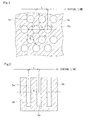
- Fig. 1 is an enlarged (part) view showing the pattern electrode formed to have a mesh-shaped conductive portion 5b in which a plurality of opening portions, each of which has a circular shape, are arranged, that is, a plurality of circular holes 5c are arranged within a flat area.
- a mesh-shaped conductive portion 5b in which a plurality of opening portions, each of which has a circular shape, are arranged, that is, a plurality of circular holes 5c are arranged within a flat area.
- the shortest distance X between mutually adjacent opening portions (circular holes 5c) of the plurality of opening portions (circular holes 5c) is assumed to be a shortest distance between the circular hole "A" and a circular hole B which is one of adj acent circular holes closest to the circular hole "A".
- the adjacent circular holes closest to the circular hole "A” are a circular hole C, a circular hole D, a circular hole E, a circular hole F, and a circular hole G which are located at the shortest distance X from the circular hole "A", in addition the circular hole B.
- the adjacent circular hole H is not located closest to the circular hole "A", so the circular hole H is eliminated from consideration.
- the length L of the line segment formed by the feet of the perpendiculars when the barycenters of the adjacent opening portions are projected to the virtual line which is the straight line parallel to the shortest distance X is the length L of the segment formed by intersections between each of perpendiculars and a virtual line "1" when the barycenter of the circular hole "A” and the barycenter of the circular hole B are projected to the virtual line "1" which is a straight line parallel to the shortest distance X between the circular hole "A" and the circular hole B in, for example, Fig. 1 .
- Fig. 2 is an enlarged (part) view showing the pattern electrode formed to have a comb-shaped conductive portion 5b in which a plurality of rectangular opening portions 5a, each of which are opened at one end, are arranged.
- the plurality of rectangular opening portions, which are opened at one end may be arranged to form the pattern electrode.
- the shortest distance X between the adjacent opening portions 5a is determined first.
- the straight line 1 parallel to the shortest distance X is assumed to be the virtual line and the barycenters of the adjacent opening portions 5a are projected to the virtual line "1". Therefore, the length L of the line segment formed by the intersections between each of the perpendiculars at the time of projection and the virtual line "1" is desirably obtained.
- the shortest distance X and the length L of the line segment are desirably obtained based on the methods described in Figs. 1 and 2 .
- the shapes of the opening portions for forming the pattern electrode and the arrangement method thereof are not particularly limited. However, for example, in the case of the pattern electrode formed to have the mesh-shaped conductive portion in which the plurality of opening portions are arranged, as shown in Fig. 1 , the opening portions are preferably arranged such that the barycenters of at least the adj acent opening portions are located on a straight line including a line corresponding to the shortest distance X between the adjacent opening portions.
- the opening portions are more preferably arranged at predetermined regular intervals such that the barycenters of opening portions other than the adjacent opening portions and not directly adjacent to each other are located on the straight line including the line corresponding to the shortest distance X. All opening portions within the flat area of the pattern electrode are further preferably arranged at predetermined regular intervals.
- the shapes of the opening portions are preferably made equal to one another are such that the barycenters of the opening portions other than the adjacent opening portions are located on the straight line including the line corresponding to the shortest distance X between the adjacent opening portions.
- the shortest distance X and the length L of the line segment are obtained based on a subject which substantially act as the opening portion.
- the first electrode layer in the present invention at least a part of the first electrode layer is preferably located corresponding to the openingportions such that the potential can penetrate through the opening portions of the pattern electrode forming the second insulating layer.
- the first electrode layer is preferably located in all portions corresponding to the opening portions.
- the first electrode layer may be formed from the pattern electrode having the mesh-shaped or comb-shaped conductive portion as in the case of the second electrode layer. However, when the ease of producing and the like are taken into account, the entire flat area is preferably the conductive portion.
- a material of each of the first electrode layer and the second electrode layer may include copper, tungsten, aluminum, nickel, chromium, silver, platinum, tin, molybdenum, magnesium, palladium, or tantalum. Copper or aluminum is preferably used in view of conductivity or productivity.
- the materials of the first electrode layer and the second electrode layer may be the same or different from each other.
- a film thickness of each of the first electrode layer and the second electrode layer can be selected as appropriate and is preferably 0.1 ⁇ m to 20 ⁇ m. In particular, the film thickness of the second electrode layer is further preferably 0.1 ⁇ m to 5 ⁇ m.
- the unevenness of the pattern electrode is reflected on the surface of the second insulating layer forming the sample chucking surface.
- the flatness of the sample chucking surface canbe maintained to Ra of approximately 1 ⁇ m without the need of special processing such as lapping.
- Each of the first electrode layer and the second electrode layer may be formed to have a predetermined-shaped conductive portion using a foil made of any one of the metals described above or formed to have a predetermined conductive portion by etching or the like using a laminate in which the metal foil is laminated on each of front and rear surfaces of an insulating film.
- the metal film may be formed on the surface of any one of the first insulating layer, the interelectrode insulating layer, or the second insulating layer by a sputtering method, an ion plating method (ion plating evaporation method) , a vapor phase growth method, plating processing, or the like and then etched in a predetermined shape if necessary to form the conductive portion.
- a metal paste may be printed on a predetermined surface to form the conductive portion.
- a high-melting point metal such as molybdenum, tungsten, or tantalum may be thermally sprayed onto a predetermined surface to form the conductive portion.
- the ion plating method is suitably used.
- Each of the first insulating layer, the interelectrode insulating layer, and the second insulating layer may be a resin layer made of one or plural kinds of resins selected from, for example, polyimide, polyamide, polyester, polyethylene terephthalate, epoxy, and acrylic, a ceramic layer made of one or plural kinds of materials selected from aluminum oxide, aluminum nitride, silicon carbide, silicon nitride, zirconia, and titania, or a layer made of one or two kinds of materials selected from silicon and silicon dioxide.
- a resin layer made of one or plural kinds of resins selected from polyimide, polyamide, polyester, polyethylene terephthalate, and epoxy may be preferably used in view of mass productivity.
- polyimide is further preferably used.
- the first insulating layer, the interelectrode insulating layer, and the second insulating layer may be made of the same material or different materials selected as appropriate.
- the respective film thicknesses can be selected as appropriate. However, it is preferable to set the thickness of the first insulating layer to 25 ⁇ m to 100 ⁇ m, set the thickness of the interelectrode layer to 25 ⁇ m to 100 ⁇ m, and set the thickness of the second insulating layer to 50 ⁇ m to 300 ⁇ m.
- an aluminum base made of an aluminum alloy which is normally used can be employed as the metal base.
- a flexible layer which has a film thickness of 500 ⁇ m to 1000 ⁇ m and is made of a silicone rubber may be provided between the metal base and the first insulating layer.
- the second insulating layer forming the sample chucking surface is made of an elastic material such as a rubber
- a contact ratio degree of contact
- the second insulating layer is made of polyimide, the contact ratio may be reduced to approximately 1%.
- the contact ratio between the sample chucking surface and the substrate can be improved.
- the second insulating layer is made of polyimide, a lower limit of the contact ratio can be increased to approximately 2%.
- a method of producing the electrostatic chuck according to the present invention is not particularly limited.
- the electrostatic chuck having the laminate structure may be formed by successively laminating the first insulating layer, the first electrode layer, the interelectrode insulating layer, the second electrode layer, and the second insulating layer on the metal base in the order of increasing distance from the metal base, then sandwiching the flexible layer between the metal base and the first insulating layer if necessary, and performing thermo compression bonding under predetermined heating and pressurization conditions.
- the electrostatic chuck having the laminate structure maybe formed by forming, in advance, the electrode sheet in which the first insulating layer, the first electrode layer, the interelectrode insulating layer, the second electrode layer, and the second insulating layer are successively laminated, then sandwiching the flexible layer between the electrode sheet and the metal base if necessary, and performing thermo compression bonding under predetermined heating and pressurization conditions.
- the first electrode layer and the second electrode layer may be integrally formed in advance with any one of the first insulating layer, the interelectrode insulating layer, and the second insulating layer and the thermo compression bonding may be performed to form the electrostatic chuck as described above.
- the shape of the electrostatic chuck in the present invention, the size thereof, and the like are not particularly limited. That is, for example, a flat shape of the sample chucking surface can be designed to have a circular shape or a rectangular shape as appropriate corresponding to the shape of the substrate which is an object to be attracted, the size thereof, and the like.
- the shape of the pattern electrode forming the second electrode layer is specified, so the penetration potential from the first electrode layer, which is distributed on the sample chucking surface side can be optimized. Therefore, it is possible to obtain the electrostatic chuck which efficiently generates the gradient force on the sample chucking surface to exercise the excellent chucking force and the excellent holding force.
- the second electrode layer located on the sample chucking surface side includes the pattern electrode having the predetermined opening portions, so a Coulomb force acts in addition to the gradient force. Therefore, the excellent chucking force and the excellent holding force can be exercised to any one of a semiconductor substrate such as a silicon wafer and an insulating substrate such as a glass substrate.
- Such an electrostatic chuck is sufficiently adaptable to the requirement for an increase in size of the held substrate. Further, the contact characteristic of the substrate to the sample chucking surface can be improved, so the substrate can be efficiently cooled.
- x bipolar electrostatic chuck
- 1 metal base
- 2 first insulating layer
- 3 first electrode layer
- 4 interelectrode insulating layer
- 5 second electrode layer (pattern electrode)
- 5a opening portion
- 5b conductive portion
- 5c circular holes
- 6 second insulating layer
- 7 sample chucking surface
- 8 substrate
- 9 electrode sheet.
- a second electrode layer is a pattern electrode in which a plurality of rectangular opening portions, which are opened at one end, are arranged to form a comb-shaped conductive portion and the barycenters of opening portions other than adjacent opening portions are located on a straight line including a line corresponding to a shortest distance X between the adj acent opening portions.
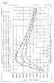
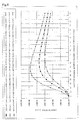
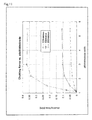
- a relationship between the shortest distance X between the adjacent opening portions and a chucking force in the case where the pattern electrode is used for the electrostatic chuck is examined. As shown in Figs.
- the entire flat area of the first electrode layer 3 is assumed to be a conductive portion, a thickness of the first electrode layer 3 and the second electrode layer 5 is set to 10 ⁇ m, and a potential difference between the electrode layers is set to 3000 V.
- Each of the interelectrode insulating layer 4 and the second insulating layer 6 is assumed to be made of polyimide.
- a dielectric constant of the second insulating layer 6 is set to 3.5 for calculation.
- An attracted/held substrate 8 is a glass substrate whose thickness is 0.5 mm and dielectric constant is 5.5. Two-dimensional general-purpose electromagnetic field calculation software is used for calculation. Fig.
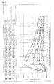
- Fig. 5 shows a relationship between the shortest distance X and the chucking force in a case where a film thickness of the second insulating layer 6 is changed to 50 ⁇ m, 75 ⁇ m, 125 ⁇ m, 150 ⁇ m, 175 ⁇ m, and 200 ⁇ m while a film thickness of the interelectrode insulating layer 4 is fixed to 50 ⁇ m.
- Fig. 6 shows a relationship between the shortest distance X and the chucking force in a case where the film thickness of the interelectrode insulating layer 4 is changed to 25 ⁇ m, 50 ⁇ m, and 75 ⁇ m while the film thickness of the second insulating layer 6 is fixed to 125 ⁇ m.
- Fig. 5 also shows a part of a result obtained by calculation in a case where a dielectric constant is set to 9 on the assumption that the second insulating layer 6 is made of ceramic.
- a peak of the chucking force appears in a range of 0.3 mm to 1.0 mm.
- the position of the peak of the chucking force is shifted in a direction in which the shortest distance X becomes shorter as the film thickness of the second insulating layer 6 becomes smaller.
- the dielectric constant of the second insulating layer 6 becomes higher, it is difficult that an electric field from the first electrode layer 3 penetrates through the opening portions 5a. Therefore, it is apparent that the peak of the chucking force is shifted in a direction in which the shortest distance X becomes longer.
- the second electrode layer 5 is a pattern electrode in which a plurality of circular holes 5c are arranged within a flat area to form a mesh-shaped conductive portion 5b.
- a relationship between the shortest distance X between the adjacent circular holes 5c and the chucking force on the sample chucking surface 7 in a case where the pattern electrode is used for the electrostatic chuck is examined.
- the circular holes 5c when attention is focused on a circular hole "A", six circular holes B to G adjacent to the circular hole "A" are arranged such that the centers of the six circular holes are located at the vertices of a regular hexagon.
- Fig. 7 shows a relationship between the shortest distance X and the chucking force in the case where a film thickness of the second insulating layer 6 is changed to 50 ⁇ m, 75 ⁇ m, 125 ⁇ m, 150 ⁇ m, 175 ⁇ m, and 200 ⁇ m while a film thickness of the interelectrode insulating layer 4 is fixed to 50 ⁇ m.
- Fig. 8 shows a relationship between the shortest distance X and the chucking force in the case where the film thickness of the interelectrode insulating layer 4 is changed to 25 ⁇ m, 50 ⁇ m, and 75 ⁇ m while the film thickness of the second insulating layer 6 is fixed to 125 ⁇ m.
- Fig. 7 also shows a part of a result obtained by calculation in the case where a dielectric constant is set to 9 on the assumption that the second insulating layer 6 is made of ceramic.
- a peak of the chucking force appears in a range of 0.3 mm to 1.2 mm.
- the position of the peak of the chucking force is shifted in a direction in which the shortest distance X becomes shorter as the film thickness of the second insulating layer 6 becomes smaller.
- the dielectric constant of the second insulating layer 6 becomes higher, it is difficult that an electric field from the first electrode layer 3 penetrates through the circular holes 5c. Therefore, it is apparent that the peak of the chucking force is shifted in a direction in which the shortest distance X becomes longer.
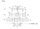
- a relationship between a value L/X and the chucking force is calculated.
- the value L/X is obtained based on the shortest distance X between the adjacent opening portions 5a and a length L of a line segment.
- a straight line parallel to the shortest distance X is assumed to be a virtual line 1
- the line segment is formed by the feet of perpendiculars in a case where the barycenters of the adj acent opening portions 5a are projected to the vertical line.
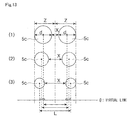
- Fig. 9 is a partially enlarged view showing the pattern electrode having the comb-shaped conductive portion 5b.
- the shortest distance X between the adjacent opening portions 5a (which corresponds to a width of one of band-like electrode portions of the comb-shaped conductive portion) and the width d of the each of the opening portions 5a are adjusted.
- Fig. 9 ((1) to (3)) shows a condition in which the width d of each of the opening portions 5a slightly changes as the shortest distance X between the adjacent opening portions 5a significantly changes in the order of (1), (2), and (3).
- a thickness of the interelectrode insulating layer 4 is set to 50 ⁇ m and a dielectric constant thereof is set to 3.5.
- the dielectric constant of the second insulating layer 6 is set to 3.5.
- the calculation is performed in the case where the thickness of the second insulating layer 6 is set to 50 ⁇ m, 125 ⁇ m, and 200 ⁇ m.
- Other conditions for the first insulating layer, the first electrode layer, the second electrode layer, and the glass substrate (object to be attracted) are equal to those in a first test example.
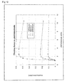
- the chucking force begins to increase at L/X equal to or larger than 1.5 and a high chucking force can be exercised in a range of L/X of 2 to 4.
- L/X becomes larger than 5
- an increase in chucking force saturates.
- a slight reduction trend occurs. It can be observed that the trend is not almost affected by the thickness of the second insulating layer 6.
- the pattern electrode having the mesh-shaped conductive portion 5b in which the plurality of circular holes 5c are arranged within the flat area is used as the second electrode layer 5.
- the same calculation as that in the third calculation example is performed.
- a relationship between the value of L/X and the chucking force per unit area on the sample chucking surface 7 in the case where the pattern electrode is used as the second electrode layer 6 is obtained by calculation. Then, substantially the same result as that in the case of the third calculation example is obtained.
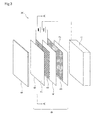
- Fig. 3 is an explanatory exploded perspective view showing a bipolar electrostatic chuck X according to a first embodiment.
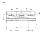
- Fig. 4 is an explanatory view showing a part of a cross-section A-A' of the bipolar electrostatic chuck X shown in Fig. 3 .
- a polyimide sheet which is 206 mm long and 206 mm wide is employed in which a copper surface layer having a film thickness of 12 ⁇ m is provided on a surface of a polyimide layer (name of product manufactured by Mitsui Chemicals, Inc.: NEOFLEX).
- the polyimide layer (50 ⁇ m in film thickness and 3.5 in dielectric constant) is provided as the interelectrode insulating layer 4.
- An outer edge of the copper surface layer is removed by etching to form the first electrode layer 3 (200 mm long and 200 mm wide) in which the entire flat area corresponds to the conductive portion.
- a chromium film is deposited at 0.1 ⁇ m on the surface of the polyimide layer (interelectrode insulating layer 4) of the polyimide sheet and a copper film whose film thickness is 0.4 ⁇ m is formed on the chromium film by an ion plating method.
- a surface of the formed copper film is subjected to predetermined mask processing and then etching processing is performed. As a result, as shown in Fig.
- the pattern electrode having the comb-shaped conductive portion 5b in which the plurality of rectangular opening portions 5a, which are opened at one end, are arranged is formed.
- the pattern electrode is used as the second electrode layer 5.
- the opening portions 5a are regularly arranged within the flat area of 200 mm long and 200 mm wide such that the opening width d of each of the opening portions 5a is 1 mm, and the shortest distance X between the adjacent opening portions 5a is 1 mm, and the barycenters of opening portions 5a other than adjacent opening portions are located on a straight line including a line corresponding to the shortest distance X between the adjacent opening portions 5a.
- the second insulating layer 6 which is a polyimide film whose length is 206 mm, width is 206 mm, film thickness is 125 ⁇ m, and dielectric constant is 3.5 (name of product manufactured by Du Pont-Toray Co., Ltd.: Kapton) is laminated on the surface of the pattern electrode forming the second electrode layer 5 through a thermoplastic polyamide adhesive sheet whose film thickness is 20 ⁇ m (not shown).
- the first insulating layer 2 which is a polyimide film whose length is 206 mm, width is 206 mm, film thickness is 40 ⁇ m, and dielectric constant is 3.5 (name of product manufactured by Du Pont-Toray Co., Ltd.: Kapton) is laminated on the surface of the first electrode layer 3 through the adhesive sheet (not shown) .
- a cushion material (not shown) is laminated on each of an upper surface side of the second insulating layer 6 and a lower surface side of the first insulating layer 2. Then, the resultant laminate is set in a hot press and heated and pressurized under a condition in which a thickness direction pressure is 2 MPa, a heat temperature is 150°C, and a holding time is 5 minutes. After that, the cushion materials are removed to produce an electrode sheet 9 having the laminate structure in which the first insulating layer 2, the first electrode layer 3, the interelectrode insulating layer 4, the second electrode layer 5, and the second insulating layer 6 are successively laminated.
- the obtained electrode sheet 9 is bonded to the aluminum base 1 which is made of an aluminum alloy (A5056) and includes a water-cooled tube which is not shown.
- the electrode sheet 9 is laminated on a surface of a porous ceramic (not shown) whose flatness is maintained with a state in which the second insulating layer 6 of the electrode sheet 9 is opposed to the porous ceramic.
- the aluminum base is provided on the first insulating layer 2 of the electrode sheet 9 through spacers (not shown), each of which is 0.7 in height and 5 mm in diameter and made of a flexible material.
- a self-adhesive liquid silicone rubber (name of product manufactured by GE Toshiba Silicones Co., Ltd: TSE3663) (not shown) is injected to a gap between the aluminum base 1 and the electrode sheet 9 which is formed by the spacers and degassing is performed under a vacuum. Then, vacuuming is performed through the porous ceramic to bring the electrode sheet 9 into sufficient contact with the surface of the porous ceramic. It takes approximately twenty-four hours to cure the silicone rubber. Therefore, the bipolar electrostatic chuck X is completed in which the electrode sheet 9 is laminated on the aluminum base through a flexible layer (not shown) which is made of a silicone rubber and has a thickness of 0. 7 mm.
- the surface (sample chucking surface 7) of the second insulating layer 6 in the completed electrostatic chuck X is surface unevenness of up to approximately ⁇ 1 ⁇ m, so lapping is not particularly required.
- the polyimide sheet (name of product manufactured by Mitsui Chemicals, Inc. : NEOFLEX) is used as in the case of the first embodiment and cut off at a diameter of 184 mm.
- the polyimide layer is provided as the interelectrode insulating layer 4.
- the outer edge of the copper surface layer is removed by etching to form the first electrode layer 3 having a diameter of 182 mm in which the entire flat area corresponds to the conductive portion.
- a chromium film is deposited at 0.1 ⁇ m on the surface of the polyimide layer (interelectrode insulating layer 4) of the polyimide sheet and a copper film whose film thickness is 0.4 ⁇ m is formed on the chromium film by an ion plating method.
- the pattern electrode having the mesh-shaped conductive portion 5b in which the plurality of circular holes 5c each having a diameter d of 1.2 mm are provided is formed.
- the pattern electrode is used as the second electrode layer 5.
- the plurality of circular holes 5c are regularly arranged within the flat area whose diameter is 182 mm.
- six of the circular holes 5c which are adjacent to the one of the circular holes 5c are arranged such that the centers of the six circular holes 5c correspond to the vertices of the regular hexagon.
- the shortest distance X between the adjacent circular holes 5c is 1.0 mm.
- the electrode sheet 9 is produced as in the first embodiment and then the bipolar electrostatic chuck X is completed as in the first embodiment.
- the chucking force of the bipolar electrostatic chuck X obtained in each of the first embodiment and the second embodiment is evaluated.
- a test silicon wafer whose size is 20 mm x 20 mm is prepared from a silicon wafer whose thickness is 0.75 mm and placed in the center of the sample chucking surface 7 of the electrostatic chuck X which is obtained in each of the first embodiment and the second embodiment and provided under a vacuum of 800 mTorr.
- a voltage difference of 3000 V is applied between the first electrode layer 3 and the second electrode layer 5 to attract the test silicon wafer.
- a chucking strength in the case where the test silicon wafer is pulled at a speed of 0.5 mm/minute in a perpendicular direction to the chucking surface under room temperature is measured by a load cell.
- a time for attracting the test silicon wafer is set to one minute.
- the same measurement is performed on a test glass substrate (5.5 in dielectric constant) whose length is 20 mm, width is 20 mm, and film thickness is 0.7 ⁇ m. Table 1 shows respective results.
- a substrate temperature in the case where the electrostatic chuck X obtained in the second embodiment is actually used for an ion implanting device is evaluated.
- the electrostatic chuck X obtained in the second embodiment is set in a hybrid scan type ion implanting device.
- a voltage difference of 3000 V is applied between the first electrode layer 3 and the second electrode layer 5 to attract a silicon wafer 8 having a diameter of 200 mm to the sample chucking surface 7 of the electrostatic chuck X.
- ion implantation is performed on the silicon wafer 8 at an ion beam power of 450 W and an ion implantation dose of 1E15 ions/cm.
- thermo-labels are attached to the center of the silicon wafer 8 and four points on the circumference of a circle whose diameter is 110 mm, that is, five locations in total and then temperatures are measured at the respective locations.
- an average temperature of the five locations is 90°C.
- the silicon wafer is attracted to the electrostatic chuck produced in the same way as in the second embodiment except for the fact that the flexible layer made of silicone rubber is not provided. Then, the temperature of the silicon wafer in the case where the ion implantation is performed under the same condition as above is measured. As a result, it is found that the average temperature of the five locations is equal to or larger than 120°C.
- the flexible layer provided in the electrostatic chuck X in each of the first embodiment and the second embodiment premises that a virtual press contactor having a width of 10 mm sinks by 0.1 ⁇ m or more (0.3 ⁇ m in maximum) in the case where the silicone rubber (hardness is 0.01GPa in Young's modulus) is used and the chucking force is set to 50 gf/cm 2 .
- a virtual press contactor having a width of 10 mm sinks by 0.1 ⁇ m or more (0.3 ⁇ m in maximum) in the case where the silicone rubber (hardness is 0.01GPa in Young's modulus) is used and the chucking force is set to 50 gf/cm 2 .
- the degree of contact between the sample chucking surface 7 of the electrostatic chuck X obtained in the second embodiment and the wafer may be approximately 10%.
Landscapes
- Container, Conveyance, Adherence, Positioning, Of Wafer (AREA)
- Jigs For Machine Tools (AREA)
Applications Claiming Priority (3)
| Application Number | Priority Date | Filing Date | Title |
|---|---|---|---|
| JP2005200739 | 2005-07-08 | ||
| JP2005357641 | 2005-12-12 | ||
| PCT/JP2006/313586 WO2007007674A1 (fr) | 2005-07-08 | 2006-07-07 | Mandrin électrostatique et feuille d’électrode pour mandrin électrostatique |
Publications (3)
| Publication Number | Publication Date |
|---|---|
| EP1909308A1 true EP1909308A1 (fr) | 2008-04-09 |
| EP1909308A4 EP1909308A4 (fr) | 2010-11-10 |
| EP1909308B1 EP1909308B1 (fr) | 2013-02-27 |
Family
ID=37637067
Family Applications (1)
| Application Number | Title | Priority Date | Filing Date |
|---|---|---|---|
| EP06767996A Not-in-force EP1909308B1 (fr) | 2005-07-08 | 2006-07-07 | Feuille d'électrode pour mandrin électrostatique |
Country Status (7)
| Country | Link |
|---|---|
| US (1) | US8158238B2 (fr) |
| EP (1) | EP1909308B1 (fr) |
| JP (1) | JP4928454B2 (fr) |
| KR (1) | KR100976320B1 (fr) |
| CN (1) | CN101218668B (fr) |
| TW (1) | TWI431707B (fr) |
| WO (1) | WO2007007674A1 (fr) |
Cited By (5)
| Publication number | Priority date | Publication date | Assignee | Title |
|---|---|---|---|---|
| WO2012123188A1 (fr) | 2011-03-17 | 2012-09-20 | Asml Netherlands B.V. | Pince électrostatique, appareil lithographique et procédé de fabrication de dispositif |
| US10483878B2 (en) | 2016-04-13 | 2019-11-19 | Trumpf Gmbh + Co. Kg | Electro-adhesion grippers with fractal electrodes |
| WO2022221050A1 (fr) * | 2021-04-16 | 2022-10-20 | Black & Decker Inc. | Embrayage électrostatique pour outil électrique |
| EP4414082A4 (fr) * | 2021-10-06 | 2025-10-15 | Creative Tech Corp | Précipitateur électrique pour moule de presse et moule de presse l'utilisant |
| EP4414083A4 (fr) * | 2021-10-06 | 2025-10-22 | Creative Tech Corp | Collecteur de poussière électrique et procédé de collecte de poussière l'utilisant |
Families Citing this family (14)
| Publication number | Priority date | Publication date | Assignee | Title |
|---|---|---|---|---|
| JP4766156B2 (ja) * | 2009-06-11 | 2011-09-07 | 日新イオン機器株式会社 | イオン注入装置 |
| BR112013011538A2 (pt) | 2010-11-11 | 2020-08-04 | Koninklijke Philips Electronics N.V. | estojo de transporte articulado para um desfibrilador portátil |
| JP5583877B1 (ja) * | 2012-11-06 | 2014-09-03 | 日本碍子株式会社 | サセプタ |
| TWI540944B (zh) * | 2014-07-14 | 2016-07-01 | 啟碁科技股份有限公司 | 基板結構的製造方法、基板結構以及金屬構件 |
| JP6334338B2 (ja) * | 2014-09-09 | 2018-05-30 | 京セラ株式会社 | 試料保持具 |
| US10355624B2 (en) * | 2014-10-09 | 2019-07-16 | Carnegie Mellon University | Electrostatic clutch |
| KR102311586B1 (ko) * | 2014-12-26 | 2021-10-12 | 삼성디스플레이 주식회사 | 증착 장치 및 증착 장치 내 기판 정렬 방법 |
| US20180138831A1 (en) * | 2016-11-17 | 2018-05-17 | Immersion Corporation | Control of Contact Conditions For Static ESF |
| KR102644838B1 (ko) * | 2018-10-23 | 2024-03-11 | 삼성디스플레이 주식회사 | 정전척 및 그를 구비하는 정전흡착장치 |
| CN112117229A (zh) * | 2019-06-20 | 2020-12-22 | 新光电气工业株式会社 | 静电吸盘和衬底固定装置 |
| KR102849923B1 (ko) * | 2020-06-24 | 2025-08-26 | 삼성디스플레이 주식회사 | 정전 척, 이를 포함하는 타일드 정전 척 및 정전 척의 제조방법 |
| US20240087839A1 (en) * | 2022-09-13 | 2024-03-14 | Applied Materials, Inc. | Managing beam power effects by varying base emissivity |
| CN119419162B (zh) * | 2024-10-18 | 2025-12-09 | 上海玄亨科技股份有限公司 | 一种复合陶瓷静电吸盘及其制造方法 |
| CN119912273B (zh) * | 2025-01-20 | 2025-11-18 | 东莞市夏阳新材料有限公司 | 一种孔隙梯度分布多孔吸盘及其制备方法 |
Family Cites Families (14)
| Publication number | Priority date | Publication date | Assignee | Title |
|---|---|---|---|---|
| US5838529A (en) | 1995-12-22 | 1998-11-17 | Lam Research Corporation | Low voltage electrostatic clamp for substrates such as dielectric substrates |
| JP3527823B2 (ja) | 1997-01-31 | 2004-05-17 | 京セラ株式会社 | 静電チャック |
| TW492135B (en) * | 2000-05-25 | 2002-06-21 | Tomoegawa Paper Co Ltd | Adhesive sheets for static electricity chuck device, and static electricity chuck device |
| JP3979792B2 (ja) * | 2000-05-25 | 2007-09-19 | 株式会社巴川製紙所 | 静電チャック装置用接着シート及び静電チャック装置 |
| JP2002026113A (ja) * | 2000-07-10 | 2002-01-25 | Toshiba Corp | ホットプレート及び半導体装置の製造方法 |
| JP4567249B2 (ja) * | 2001-09-04 | 2010-10-20 | 太平洋セメント株式会社 | 静電チャック |
| JP2003243493A (ja) | 2002-02-15 | 2003-08-29 | Taiheiyo Cement Corp | 双極型静電チャック |
| JP4010541B2 (ja) * | 2002-06-18 | 2007-11-21 | キヤノンアネルバ株式会社 | 静電吸着装置 |
| JP3965469B2 (ja) * | 2002-10-30 | 2007-08-29 | 京セラ株式会社 | 静電チャック |
| US7430104B2 (en) * | 2003-03-11 | 2008-09-30 | Appiled Materials, Inc. | Electrostatic chuck for wafer metrology and inspection equipment |
| JP4057977B2 (ja) * | 2003-08-08 | 2008-03-05 | 株式会社巴川製紙所 | 静電チャック装置用電極シート、静電チャック装置および吸着方法 |
| CN100470755C (zh) * | 2004-03-19 | 2009-03-18 | 创意科技股份有限公司 | 双极型静电吸盘 |
| JP4684222B2 (ja) * | 2004-03-19 | 2011-05-18 | 株式会社クリエイティブ テクノロジー | 双極型静電チャック |
| WO2007066572A1 (fr) * | 2005-12-06 | 2007-06-14 | Creative Technology Corporation | Feuille d’électrode pour mandrin électrostatique, et mandrin électrostatique |
-
2006
- 2006-07-07 WO PCT/JP2006/313586 patent/WO2007007674A1/fr not_active Ceased
- 2006-07-07 TW TW095125093A patent/TWI431707B/zh not_active IP Right Cessation
- 2006-07-07 CN CN2006800248871A patent/CN101218668B/zh not_active Expired - Fee Related
- 2006-07-07 US US11/922,458 patent/US8158238B2/en not_active Expired - Fee Related
- 2006-07-07 KR KR1020087002976A patent/KR100976320B1/ko not_active Expired - Fee Related
- 2006-07-07 EP EP06767996A patent/EP1909308B1/fr not_active Not-in-force
- 2006-07-07 JP JP2007524629A patent/JP4928454B2/ja active Active
Cited By (8)
| Publication number | Priority date | Publication date | Assignee | Title |
|---|---|---|---|---|
| WO2012123188A1 (fr) | 2011-03-17 | 2012-09-20 | Asml Netherlands B.V. | Pince électrostatique, appareil lithographique et procédé de fabrication de dispositif |
| US9360771B2 (en) | 2011-03-17 | 2016-06-07 | Asml Netherlands B.V. | Electrostatic clamp, lithographic apparatus, and device manufacturing method |
| TWI560526B (en) * | 2011-03-17 | 2016-12-01 | Asml Netherlands Bv | Electrostatic clamp, lithographic apparatus, and device manufacturing method |
| US10483878B2 (en) | 2016-04-13 | 2019-11-19 | Trumpf Gmbh + Co. Kg | Electro-adhesion grippers with fractal electrodes |
| WO2022221050A1 (fr) * | 2021-04-16 | 2022-10-20 | Black & Decker Inc. | Embrayage électrostatique pour outil électrique |
| US12576549B2 (en) | 2021-04-16 | 2026-03-17 | Black & Decker Inc. | Electrostatic clutch for power tool |
| EP4414082A4 (fr) * | 2021-10-06 | 2025-10-15 | Creative Tech Corp | Précipitateur électrique pour moule de presse et moule de presse l'utilisant |
| EP4414083A4 (fr) * | 2021-10-06 | 2025-10-22 | Creative Tech Corp | Collecteur de poussière électrique et procédé de collecte de poussière l'utilisant |
Also Published As
| Publication number | Publication date |
|---|---|
| HK1119294A1 (en) | 2009-02-27 |
| KR20080038333A (ko) | 2008-05-06 |
| WO2007007674A1 (fr) | 2007-01-18 |
| EP1909308A4 (fr) | 2010-11-10 |
| CN101218668B (zh) | 2010-11-03 |
| JP4928454B2 (ja) | 2012-05-09 |
| TW200715447A (en) | 2007-04-16 |
| US20090041980A1 (en) | 2009-02-12 |
| CN101218668A (zh) | 2008-07-09 |
| TWI431707B (zh) | 2014-03-21 |
| KR100976320B1 (ko) | 2010-08-16 |
| JPWO2007007674A1 (ja) | 2009-01-29 |
| EP1909308B1 (fr) | 2013-02-27 |
| US8158238B2 (en) | 2012-04-17 |
Similar Documents
| Publication | Publication Date | Title |
|---|---|---|
| EP1909308B1 (fr) | Feuille d'électrode pour mandrin électrostatique | |
| US11233199B2 (en) | Vapor deposition mask manufacturing method, vapor deposition mask, and organic semiconductor element manufacturing method | |
| JP5458323B2 (ja) | 静電チャック及びその製造方法 | |
| KR101429593B1 (ko) | 교류구동 정전 척 | |
| DE112005000621B4 (de) | Bipolare elektrostatische Haltevorrichtung | |
| EP1959488A1 (fr) | Feuille d' electrode pour mandrin electrostatique, et mandrin electrostatique | |
| TW439168B (en) | Improved apparatus for retaining a workpiece upon a workpiece support and method of manufacturing same | |
| US20130070384A1 (en) | High Surface Resistivity Electrostatic Chuck | |
| DK2852987T3 (en) | Method for producing substrate for super senior lag | |
| KR20180018335A (ko) | 기판 고정 장치 및 그 제조방법 | |
| EP2915189B1 (fr) | Mandrin électrostatique possédant une surface de contact à saillie souple pouvant être configurée à la lumière | |
| KR20200143268A (ko) | 기판 고정 장치 및 그 제조 방법 | |
| JP6010720B1 (ja) | ウエハ支持構造体 | |
| WO2012026421A1 (fr) | Dispositif de mandrin électrostatique et procédé de fabrication de celui-ci | |
| EP2148360A1 (fr) | Procede de gravure a sec | |
| US20240312769A1 (en) | Ceramic assembly and electrostatic chuck device | |
| KR102633781B1 (ko) | 프레임 일체형 마스크 및 그 제조 방법 | |
| HK1119294B (en) | Electrostatic chuck and electrode sheet for electrostatic chuck | |
| JP7828225B2 (ja) | 静電チャック及びその製造方法 | |
| KR102948653B1 (ko) | 마스크와 지지부의 연결체 및 그 제조 방법 | |
| KR20240013715A (ko) | 프레임 일체형 마스크 및 그 제조 방법 | |
| KR20240039474A (ko) | 마스크와 프레임의 연결체 및 그 제조 방법 | |
| KR20240053446A (ko) | 마스크와 프레임의 연결체 및 그 제조 방법 | |
| JP2003133400A (ja) | 吸着装置、真空処理装置及び吸着装置の製造方法 | |
| JP2003045951A (ja) | 吸着装置 |
Legal Events
| Date | Code | Title | Description |
|---|---|---|---|
| PUAI | Public reference made under article 153(3) epc to a published international application that has entered the european phase |
Free format text: ORIGINAL CODE: 0009012 |
|
| 17P | Request for examination filed |
Effective date: 20080130 |
|
| AK | Designated contracting states |
Kind code of ref document: A1 Designated state(s): DE FR GB |
|
| RIC1 | Information provided on ipc code assigned before grant |
Ipc: H01L 21/683 20060101AFI20080519BHEP |
|
| DAX | Request for extension of the european patent (deleted) | ||
| RBV | Designated contracting states (corrected) |
Designated state(s): DE FR GB |
|
| A4 | Supplementary search report drawn up and despatched |
Effective date: 20101013 |
|
| RIC1 | Information provided on ipc code assigned before grant |
Ipc: H02N 13/00 20060101ALI20101007BHEP Ipc: H01L 21/683 20060101AFI20080519BHEP |
|
| 17Q | First examination report despatched |
Effective date: 20110608 |
|
| RTI1 | Title (correction) |
Free format text: ELECTRODE SHEET FOR ELECTROSTATIC CHUCK |
|
| GRAP | Despatch of communication of intention to grant a patent |
Free format text: ORIGINAL CODE: EPIDOSNIGR1 |
|
| GRAS | Grant fee paid |
Free format text: ORIGINAL CODE: EPIDOSNIGR3 |
|
| GRAP | Despatch of communication of intention to grant a patent |
Free format text: ORIGINAL CODE: EPIDOSNIGR1 |
|
| GRAA | (expected) grant |
Free format text: ORIGINAL CODE: 0009210 |
|
| AK | Designated contracting states |
Kind code of ref document: B1 Designated state(s): DE FR GB |
|
| REG | Reference to a national code |
Ref country code: GB Ref legal event code: FG4D |
|
| REG | Reference to a national code |
Ref country code: DE Ref legal event code: R096 Ref document number: 602006034767 Country of ref document: DE Effective date: 20130418 |
|
| PLBE | No opposition filed within time limit |
Free format text: ORIGINAL CODE: 0009261 |
|
| STAA | Information on the status of an ep patent application or granted ep patent |
Free format text: STATUS: NO OPPOSITION FILED WITHIN TIME LIMIT |
|
| 26N | No opposition filed |
Effective date: 20131128 |
|
| REG | Reference to a national code |
Ref country code: DE Ref legal event code: R097 Ref document number: 602006034767 Country of ref document: DE Effective date: 20131128 |
|
| REG | Reference to a national code |
Ref country code: FR Ref legal event code: PLFP Year of fee payment: 11 |
|
| PGFP | Annual fee paid to national office [announced via postgrant information from national office to epo] |
Ref country code: DE Payment date: 20160801 Year of fee payment: 11 Ref country code: GB Payment date: 20160728 Year of fee payment: 11 |
|
| PGFP | Annual fee paid to national office [announced via postgrant information from national office to epo] |
Ref country code: FR Payment date: 20160723 Year of fee payment: 11 |
|
| REG | Reference to a national code |
Ref country code: DE Ref legal event code: R119 Ref document number: 602006034767 Country of ref document: DE |
|
| GBPC | Gb: european patent ceased through non-payment of renewal fee |
Effective date: 20170707 |
|
| REG | Reference to a national code |
Ref country code: FR Ref legal event code: ST Effective date: 20180330 |
|
| PG25 | Lapsed in a contracting state [announced via postgrant information from national office to epo] |
Ref country code: DE Free format text: LAPSE BECAUSE OF NON-PAYMENT OF DUE FEES Effective date: 20180201 Ref country code: GB Free format text: LAPSE BECAUSE OF NON-PAYMENT OF DUE FEES Effective date: 20170707 |
|
| PG25 | Lapsed in a contracting state [announced via postgrant information from national office to epo] |
Ref country code: FR Free format text: LAPSE BECAUSE OF NON-PAYMENT OF DUE FEES Effective date: 20170731 |