EP1909351B1 - Filtre passe-bande de type réfléchissant - Google Patents
Filtre passe-bande de type réfléchissant Download PDFInfo
- Publication number
- EP1909351B1 EP1909351B1 EP07117701A EP07117701A EP1909351B1 EP 1909351 B1 EP1909351 B1 EP 1909351B1 EP 07117701 A EP07117701 A EP 07117701A EP 07117701 A EP07117701 A EP 07117701A EP 1909351 B1 EP1909351 B1 EP 1909351B1
- Authority
- EP
- European Patent Office
- Prior art keywords
- center conductor
- ghz
- reflection
- bandpass filter
- conductors
- Prior art date
- Legal status (The legal status is an assumption and is not a legal conclusion. Google has not performed a legal analysis and makes no representation as to the accuracy of the status listed.)
- Not-in-force
Links
- 239000004020 conductor Substances 0.000 claims description 132
- 238000009826 distribution Methods 0.000 claims description 20
- 239000000758 substrate Substances 0.000 claims description 16
- 238000000034 method Methods 0.000 claims description 12
- 230000005540 biological transmission Effects 0.000 claims description 10
- 238000004891 communication Methods 0.000 claims description 7
- 239000002184 metal Substances 0.000 claims description 6
- 229910052751 metal Inorganic materials 0.000 claims description 6
- 230000003595 spectral effect Effects 0.000 claims description 6
- 238000004519 manufacturing process Methods 0.000 claims description 5
- 238000001228 spectrum Methods 0.000 claims description 3
- 230000002194 synthesizing effect Effects 0.000 claims description 2
- 230000001902 propagating effect Effects 0.000 description 4
- RYGMFSIKBFXOCR-UHFFFAOYSA-N Copper Chemical compound [Cu] RYGMFSIKBFXOCR-UHFFFAOYSA-N 0.000 description 3
- 229910052802 copper Inorganic materials 0.000 description 3
- 239000010949 copper Substances 0.000 description 3
- 230000008878 coupling Effects 0.000 description 3
- 238000010168 coupling process Methods 0.000 description 3
- 238000005859 coupling reaction Methods 0.000 description 3
- 238000005516 engineering process Methods 0.000 description 2
- 230000015572 biosynthetic process Effects 0.000 description 1
- 230000003247 decreasing effect Effects 0.000 description 1
- 239000000463 material Substances 0.000 description 1
- 230000035699 permeability Effects 0.000 description 1
- 230000008569 process Effects 0.000 description 1
- 238000006467 substitution reaction Methods 0.000 description 1
- 238000003786 synthesis reaction Methods 0.000 description 1
- 230000009466 transformation Effects 0.000 description 1
- 230000007704 transition Effects 0.000 description 1
Images





Classifications
-
- H—ELECTRICITY
- H01—ELECTRIC ELEMENTS
- H01P—WAVEGUIDES; RESONATORS, LINES, OR OTHER DEVICES OF THE WAVEGUIDE TYPE
- H01P1/00—Auxiliary devices
- H01P1/20—Frequency-selective devices, e.g. filters
- H01P1/201—Filters for transverse electromagnetic waves
- H01P1/203—Strip line filters
-
- H—ELECTRICITY
- H01—ELECTRIC ELEMENTS
- H01P—WAVEGUIDES; RESONATORS, LINES, OR OTHER DEVICES OF THE WAVEGUIDE TYPE
- H01P1/00—Auxiliary devices
- H01P1/20—Frequency-selective devices, e.g. filters
- H01P1/201—Filters for transverse electromagnetic waves
- H01P1/2013—Coplanar line filters
Definitions
- This invention relates to a reflection-type bandpass filter for use in ultra-wideband (UWB) wireless data communication.
- UWB ultra-wideband
- This invention relates to a reflection-type bandpass filter for use in ultra-wideband (hereafter "UWB”) wireless data communication.
- UWB ultra-wideband
- bandpass filters proposed in the prior art may not satisfy the FCC specifications, due to manufacturing tolerances and other reasons.
- bandpass filters which use coplanar strips do not use wide ground strips, and so are not suitable for coupling with transmission lines such as slot lines.
- This invention was devised in light of the above circumstances, and has as an object the provision of a high-performance UWB reflection-type bandpass filter which has excellent coupling characteristics with transmission lines such as slot lines, and which satisfies FCC specifications.
- This invention provides a reflection-type bandpass filter for ultra-wideband wireless data communication, in which are provided on the surface of a dielectric substrate a center conductor and side conductors provided on both sides of the center conductor securing a prescribed distance between conductors with non-conducting portions intervening, and in which one of the center conductor width and the distances between conductors is distributed non-uniformly in a length direction of the center conductor, and the other of the center conductor width and the distances between conductors is constant, with the additional features of claim 1.
- the invention also provides a method for manufacturing a reflection-type bandpass filter for ultra-wideband wireless data communication, in accordance with claim 9.
- the center conductor width may be constant, and the distances between conductors may be distributed non-uniformly.
- the distances between conductors may be constant, and the center conductor width may be distributed non-uniformly.
- a difference of 10 dB or higher may exist between a reflectance in a ranges of frequencies f for which f ⁇ 3.1 GHz and f > 10.6 GHz, and a reflectance in a range of frequencies 3.9 GHz ⁇ f ⁇ 9.8 GHz, and in a range 3.9 GHz ⁇ f ⁇ 9.8 GHz a group delay variation may be within ⁇ 0.1 ns.
- a difference of 10 dB or higher may exist between a reflectance in a range of frequencies f for which f ⁇ 3.1 GHz and f > 10.6 GHz, and a reflectance in a range of frequencies 3.7 GHz ⁇ f ⁇ 10.0 GHz, and in a range 3.7 GHz ⁇ f ⁇ 10.0 GHz a group delay variation may be within ⁇ 0.1 ns.
- a difference of 10 dB or higher may exist between a reflectance in a range of frequencies f for which f ⁇ 3.1 GHz and f > 10.6 GHz, and a reflectance in a range of frequencies 4.1 GHz ⁇ f ⁇ 9.5 GHz, and in a range 4.1 GHz ⁇ f ⁇ 9.5 GHz a group delay variation may be within ⁇ 0.1 ns.
- a characteristic impedance Zc of an input terminal transmission line may be in the range 10 ⁇ ⁇ Zc ⁇ 300 ⁇ .
- a resistance having the same impedance as the above characteristic impedance value, or a non-reflecting terminator, may be provided on the terminating side.
- the dielectric substrate may have a thickness h in a range 0.1 mm ⁇ h ⁇ 10 mm, a relative permittivity ⁇ r in a range 1 ⁇ ⁇ r ⁇ 500, a width W in a range 2 mm ⁇ W ⁇ 100 mm, and a length L in a range 2 mm ⁇ L ⁇ 500 mm.
- length-direction distributions of the center conductor width and of the distances between conductors may satisfy a design method based on the inverse problem of deriving a potential from spectral data in the Zakharov-Shabat equation.
- length-direction distributions of the center conductor width and of the distances between conductors may satisfy a window function method.
- length-direction distributions of the center conductor width and of the distances between conductors may satisfy a Kaiser window function method.
- a reflection-type bandpass filter of this invention by applying a window function technique to design a reflection-type bandpass filter comprising non-uniform coplanar strips, the pass band can be made extremely broad and variation in group delay within the pass band can be made extremely small compared with filters of the related art, even when manufacturing tolerances are large. As a result, a UWB bandpass filter can be provided which satisfies FCC specifications.
- ground strips can be made wide, so that easy coupling with transmission lines such as slot lines is achieved.
- ground strips refers to the conductors on both sides, which are connected together on the input end.
- Fig. 1 is a perspective view showing, in summary, the configuration of a reflection-type bandpass filter of an exemplary aspect of this invention.
- the symbol 1 is the reflection-type bandpass filter
- 2 is a dielectric substrate
- 3 is a center conductor
- 4a and 4b are non-conducting portions
- 5a and 5b are side conductors.
- the center conductor 3 and side conductors 5a, 5b provided on either side of the center conductor 3, maintaining a prescribed distance between conductors and with non-conducting portions 4a, 4b intervening, are formed on the surface of the dielectric substrate 2; the non-uniform coplanar strips are such that the center conductor width or the distances between conductors, or both, are distributed non-uniformly in the length direction of the center conductor 3.
- the z axis is taken along the length direction of the center conductor 3
- the y axis is taken in the direction perpendicular to the z axis and parallel to the surface of the substrate 2
- the x axis is taken in the direction perpendicular to the y axis and to the z axis.
- the length extending in the z axis direction from the end face on the input end is z.
- the conductor-to-conductor distance between the side conductor 5a and the center conductor 3, and the conductor-to-conductor distance between the side conductor 5b and the center conductor 3, are the same at each place where z is equal (hereafter the "distance between conductors s").
- the side conductors 5a and 5b are semi-infinite: in other words, the widths of the side conductors 5a and 5b are ten times or greater than the width of the center conductor 3 and the non-conducting portions 4a, 4b.
- the side conductors 5a, 5b can be used in configuring a slot line, slot antenna, or the like.
- the characteristic impedance of this reflection-type bandpass filter is low, so that the substrate 2 can be fabricated from material with a low permittivity.
- a reflection-type bandpass filter of this aspect of the invention adopts a configuration in which stop band rejection (the difference between the reflectance in the pass band, and the reflectance in the stop band) is increased, by using a window function method (see Reference 10) employed in digital filter design.
- stop band rejection the difference between the reflectance in the pass band, and the reflectance in the stop band
- a window function method see Reference 10
- the stop band rejection can be increased.
- manufacturing tolerances can be increased.
- variation in the group delay within the pass band is decreased.
- the transmission line of a reflection-type bandpass filter 1 of this aspect of the invention can be represented by a non-uniformly distributed constant circuit such as in Fig. 19 .
- L(z) and C(z) are the inductance and capacitance respectively per unit length in the transmission line.
- the function of equation (2) is introduced.
- Z(z) ⁇ L(z)/C(z) ⁇ is the local characteristic impedance
- ⁇ 1 , ⁇ 2 are the power wave amplitudes propagating in the +z and -z directions respectively.
- c(z) 1/ ⁇ L(z)/C(z) ⁇ . If the time factor is set to exp(j ⁇ t), and a variable transformation is performed as in equation (4) below, then the Zakharov-Shabat equation of equation (5) is obtained.
- the Zakharov-Shabat inverse problem involves synthesizing the potential q(x) from spectral data which is a solution satisfying the above equations (see Reference 11). If the potential q(x) is found, the local characteristic impedance Z(x) is determined as in equation (7) below.
- Z x Z 0 exp 2 ⁇ ⁇ 0 x q s d s .
- the reflectance coefficient r(x) in x space is calculated from the spectra data reflectance coefficient R( ⁇ ) using the following equation (8), and q(x) are obtained from r(x).
- r x 1 2 ⁇ ⁇ ⁇ - ⁇ ⁇ R ⁇ ⁇ e - j ⁇ ⁇ ⁇ x d ⁇
- a window function is applied as in equation (9) to determine r'(x) .
- r ⁇ x ⁇ x ⁇ r x .
- ⁇ (x) is the window function. If the window function is selected appropriately, the stop band rejection level can be appropriately controlled.
- a Kaiser window is used as an example. The Kaiser window is defined as in equation (10) below (see Reference 10).
- ⁇ n ⁇ I 0 ⁇ ⁇ ⁇ 1 - n - ⁇ / ⁇ 2 1 ⁇ 2 I 0 ⁇ , 0 ⁇ n ⁇ M , 0 , otherwise
- ⁇ M/s, and ⁇ is determined empirically as in equation (11) below.
- ⁇ ⁇ 0.1102 ⁇ A - 8.7 , A > 50 , 0.5842 ⁇ A - 21 0.4 + 0.07886 ⁇ A - 21 , 21 ⁇ A ⁇ 50 , 0 , a ⁇ 21
- the characteristic impedance can be changed (see Reference 12).
- the center conductor width w or distance between conductors s was calculated based on the local characteristic impedance obtained from equation (7), and a bandpass filter 1 was manufactured so as to satisfy the calculated center conductor width w or distance between conductors s.
- reflection-type bandpass filters 1 having the desired pass band were obtained.
- the characteristic impedance is set so as to match the impedance of the system being used.
- a system impedance of 50 ⁇ , 75 ⁇ , 300 ⁇ , or similar is used. It is desirable that the characteristic impedance Zc be in the range 10 ⁇ ⁇ Zc ⁇ 300 ⁇ . If the characteristic impedance is smaller than 10 ⁇ , then losses due to the conductor and dielectric become comparatively large. If the characteristic impedance is higher than 300 ⁇ , matching with the system impedance is not possible.
- Fig. 4 shows the distribution in the z-axis direction of the local characteristic impedance obtained in the inverse problem.
- Tables 1 through 3 list the distances between conductors s. Table 1.
- Fig. 6 shows the shape of the coplanar strip in the reflection-type bandpass filter 1 of Embodiment 1.
- the lightly shaded portion represents the center conductor 3 and the side conductors 5a and 5b, and the heavily shaded lines represent the non-conducting portions 4a and 4b.
- the non-reflecting terminator or resistance may be connected directly to the terminating end of the reflection-type bandpass filter 1.
- ⁇ , ⁇ 0 , and ⁇ are respectively the angular frequency, magnetic permeability in vacuum, and the conductivity of the metal.
- the thickness of the center conductor 3 and of the side conductors 5a, 5b may be 2.1 ⁇ m or greater.
- This bandpass filter 1 is used in a system with a characteristic impedance of 75 ⁇ .
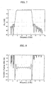
- Fig. 7 and Fig. 8 show the amplitude characteristic and group delay characteristic respectively of reflected waves (S 11 ) in the bandpass filter 1 of Embodiment 1.
- the reflectance in the range of frequencies f for which 3.9 GHz ⁇ f ⁇ 9.8 GHz, the reflectance is -2 dB or greater, and the group delay variation is within ⁇ 0.1 ns.
- the reflectance In the region f ⁇ 3.1 GHz or f > 10.6 GHz, the reflectance is -15 dB or lower.
- Fig. 9 shows the distribution in the z-axis direction of the local characteristic impedance obtained in the inverse problem.
- Tables 4 through 6 list the center conductor widths w. Table 4.
- Fig. 11 shows the shape of the coplanar strip in the reflection-type bandpass filter 1 of Embodiment 2.
- the lightly shaded portion represents the center conductor 3 and the side conductors 5a and 5b, and the heavily shaded lines represent the non-conducting portions 4a and 4b.
- the thickness of the center conductor 3 and of the side conductors 5a, 5b may be 2.1 ⁇ m or greater.
- This bandpass filter 1 is used in a system with a characteristic impedance of 75 ⁇ .
- Fig. 12 and Fig. 13 show the amplitude characteristic and group delay characteristic respectively of reflected waves (S 11 ) in the bandpass filter 1 of Embodiment 2.
- the reflectance in the range of frequencies f for which 3.7 GHz ⁇ f ⁇ 10.0 GHz, the reflectance is -5 dB or greater, and the group delay variation is within ⁇ 0.1 ns.
- the reflectance In the region f ⁇ 3.1 GHz or f > 10.6 GHz, the reflectance is -20 dB or lower.
- Fig. 14 shows the distribution in the z-axis direction of the local characteristic impedance obtained in the inverse problem.
- Table 7 lists the distances between conductors s. Table 7.
- Fig. 16 shows the shape of the coplanar strip in the reflection-type bandpass filter 1 of Embodiment 3.
- the lightly shaded portion represents the center conductor 3 and the side conductors 5a and 5b, and the heavily shaded portion represents the non-conducting portions 4a and 4b.
- the thickness of the center conductor 3 and of the side conductors 5a, 5b may be 2.1 ⁇ m or greater.
- This bandpass filter 1 is used in a system with a characteristic impedance of 50 ⁇ .
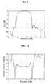
- Fig. 17 and Fig. 18 show the amplitude characteristic and group delay characteristic respectively of reflected waves (S 11 ) in the bandpass filter 1 of Embodiment 3.
- the reflectance in the range of frequencies f for which 4.1 GHz ⁇ f ⁇ 9.5 GHz, the reflectance is -5 dB or greater, and the group delay variation is within ⁇ 0.1 ns.
- the reflectance In the region f ⁇ 3.1 GHz or f > 10.6 GHz, the reflectance is -15 dB or lower.
Landscapes
- Physics & Mathematics (AREA)
- Electromagnetism (AREA)
- Control Of Motors That Do Not Use Commutators (AREA)
Claims (9)
- Filtre passe-bande de type réfléchissant pour une communication de données sans fil à bande ultralarge (1), le filtre comprenant :un substrat diélectrique (2),un conducteur central (3) et une pluralité de conducteurs latéraux (5a, 5b) pourvus des deux côtés du conducteur central, le conducteur central et les conducteurs latéraux étant disposés sur une surface du substrat diélectrique avec des parties non conductrices (4a, 4b) intermédiaires, caractérisé en ce que :l'une de la largeur du conducteur central et des distances entre conducteurs est distribuée non-uniformément dans un sens longitudinal du conducteur central, et l'autre de la largeur du conducteur central et des distances entre conducteurs est constante ;l'impédance caractéristique locale Z(x) du filtre passe-bande de type réfléchissant satisfait l'équation (1) suivante qui est l'équation de Zakharov-Shabat concernant la ligne de transmission du filtre passe-bande de type réfléchissant, et à l'équation (2) suivante ;les distributions dans le sens longitudinal de la largeur du conducteur central et des distances entre les conducteurs sont déterminées sur la base de l'impédance caractéristique locale Z(x) ;les distributions dans le sens longitudinal de la largeur du conducteur central et des distances entre conducteurs satisfont un procédé de fonction à fenêtre ; etles distributions dans le sens longitudinal de la largeur du conducteur central et des distances entre conducteurs satisfont à un procédé de fonction à fenêtre de Kaiser,

 ϕ1(x) est l'amplitude complexe de l'onde de puissance qui se propage dans le sens de la transmission du courant de ligne dans le conducteur central ;ϕ2(x) est l'amplitude complexe de l'onde de puissance qui se propage dans le sens inverse de la transmission du courant de ligne dans le conducteur central ; etq(x) est le potentiel qui est synthétisé à partir des données spectrales de ϕ1(X) et ϕ2(x) qui sont les solutions satisfaisant à l'équation (1) ci-dessus, sur la base du problème inverse de dérivation d'un potentiel à partir de données spectrales dans l'équation de Zakharov-Shabat.
 - Filtre passe-bande de type réfléchissant selon la revendication 1,
dans lequel une différence entre une réflectance du filtre dans une plage de fréquences f pour laquelle f < 3,1 GHz et f> 10,6 GHz, et une réflectance dans une plage de fréquences pour laquelle 3,9 GHz ≤ f ≤ 9,8 GHz, est de 10 dB ou supérieure, et
dans lequel, dans une plage 3,9 GHz ≤ f ≤ 9,8 GHz, une variation du temps de propagation de groupe est dans ±0,1 ns. - Filtre passe-bande de type réfléchissant selon la revendication 1,
dans lequel une différence entre une réflectance dans une plage de fréquences f pour laquelle f< 3,1 GHz et f> 10,6 GHz, et une réflectance dans une plage de fréquences pour laquelle 3,7 GHz ≤ f ≤ 10,0 GHz, est de 10 dB ou supérieure, et
dans lequel, dans une plage 3,7 GHz ≤ f ≤ 10,0 GHz, une variation du temps de propagation de groupe est dans ±0,1 ns. - Filtre passe-bande de type réfléchissant selon la revendication 1,
dans lequel une différence entre une réflectance dans une plage de fréquences f pour laquelle f< 3,1 GHz et f> 10,6 GHz, et une réflectance dans une plage de fréquences pour laquelle 4,1 GHz ≤ f ≤ 9,5 GHz, est de 10 dB ou supérieure, et
dans lequel, dans une plage 4,1 GHz ≤ f ≤ 9,5 GHz, une variation du temps de propagation de groupe est dans ±0,1 ns. - Filtre passe-bande de type réfléchissant selon la revendication 1, dans lequel une impédance caractéristique Zc d'une ligne de transmission à borne d'entrée satisfait à l'inégalité : 10 Ω ≤ Zc ≤ 300 Ω.
- Filtre passe-bande de type réfléchissant selon la revendication 5, comprenant en outre, d'un côté de terminaison, l'une parmi :une résistance ayant la même impédance que ladite valeur d'impédance caractéristique, etune terminaison non-réfléchissante.
- Filtre passe-bande de type réfléchissant selon la revendication 1, dans lequel le conducteur central et les conducteurs latéraux comprennent des plaques métalliques d'une épaisseur égale ou supérieure à une profondeur de peau à une fréquence f = 1 GHz.
- Filtre passe-bande de type réfléchissant selon la revendication 1, dans lequel le substrat diélectrique a une épaisseur h dans une plage 0,1 mm ≤ h ≤ 10 mm, une permittivité relative εr dans une plage 1 ≤ εr ≤ 500, une largeur W dans une plage 2 mm ≤ W ≤ 100 mm, et une longueur L dans une plage 2 mm ≤ L ≤ 500 mm.
- Procédé pour fabriquer un filtre passe-bande de type réfléchissant (1) pour une communication de données sans fil à bande ultralarge, le filtre passe-bande de type réfléchissant comprenant : un substrat diélectrique (2), un conducteur central (3) et une pluralité de conducteurs latéraux (5a, 5b) pourvus des deux côtés du conducteur central, le conducteur central et les conducteurs latéraux étant disposés sur une surface du substrat diélectrique avec des parties non conductrices (4a, 4b) intermédiaires, caractérisé en ce que :le procédé comprend la détermination des distributions dans le sens longitudinal de la largeur du conducteur central et des distances entre les conducteurs en :synthétisant le potentiel q(x) à partir de données spectrales de ϕ1(x) et ϕ2(x) qui sont les solutions satisfaisant l'équation (1) suivante qui est l'équation de Zakharov-Shabat concernant la ligne de transmission du filtre passe-bande de type réfléchissant ;
 déterminant le potentiel q(x) à partir de r'(x) calculé d'après l'utilisation de l'équation (2) suivante,
 où :r(x) est un coefficient de réflectance et est calculé à partir du coefficient de réflectance de données spectrales R(ω) en utilisant l'équation (3) suivante,
 ω(n) est une fonction de fenêtre de Kaiser et est calculée d'après l'utilisation de l'équation (4) suivante, et l'équation (4) satisfait les équations (5) et (6) suivantes,

 A=-20 log10δ, et δ est l'erreur d'approximation de crête dans la bande passante et dans la bande coupée ;déterminant l'impédance caractéristique locale Z(x) à partir du potentiel q(x) en utilisant l'équation (7) suivante ; et
 déterminant les distributions dans le sens longitudinal de la largeur du conducteur central et des distances entre les conducteurs sur la base de ladite impédance caractéristique locale Z(x), de sorte que l'une de la largeur du conducteur central etdes distances entre conducteurs soit distribuée non-uniformément dans un sens longitudinal du conducteur central, et que l'autre de la largeur du conducteur central et des distances entre conducteurs soit constante,où :ϕ1(x) est l'amplitude complexe de l'onde de puissance qui se propage dans le sens de la transmission du courant de ligne dans le conducteur central ; etϕ2(x) est l'amplitude complexe de l'onde de puissance qui se propage dans le sens inverse de la transmission du courant de ligne dans le conducteur central.
Applications Claiming Priority (1)
| Application Number | Priority Date | Filing Date | Title |
|---|---|---|---|
| JP2006274323A JP2008098701A (ja) | 2006-10-05 | 2006-10-05 | 反射型バンドパスフィルター |
Publications (2)
| Publication Number | Publication Date |
|---|---|
| EP1909351A1 EP1909351A1 (fr) | 2008-04-09 |
| EP1909351B1 true EP1909351B1 (fr) | 2012-04-11 |
Family
ID=38760969
Family Applications (1)
| Application Number | Title | Priority Date | Filing Date |
|---|---|---|---|
| EP07117701A Not-in-force EP1909351B1 (fr) | 2006-10-05 | 2007-10-02 | Filtre passe-bande de type réfléchissant |
Country Status (4)
| Country | Link |
|---|---|
| US (1) | US7852173B2 (fr) |
| EP (1) | EP1909351B1 (fr) |
| JP (1) | JP2008098701A (fr) |
| CN (1) | CN101159348A (fr) |
Families Citing this family (2)
| Publication number | Priority date | Publication date | Assignee | Title |
|---|---|---|---|---|
| US20100225425A1 (en) * | 2009-03-09 | 2010-09-09 | Taiwan Semiconductor Manufacturing Company, Ltd. | High performance coupled coplanar waveguides with slow-wave features |
| TWI513091B (zh) * | 2013-01-04 | 2015-12-11 | Nat Univ Tsing Hua | 寬頻帶高頻濾波器 |
Family Cites Families (28)
| Publication number | Priority date | Publication date | Assignee | Title |
|---|---|---|---|---|
| GB579414A (en) * | 1941-10-15 | 1946-08-02 | Standard Telephones Cables Ltd | Improvements in or relating to electric wave filters |
| US3617877A (en) * | 1969-07-01 | 1971-11-02 | Us Navy | Coaxial line measurement device having metal strip filter |
| US4371853A (en) * | 1979-10-30 | 1983-02-01 | Matsushita Electric Industrial Company, Limited | Strip-line resonator and a band pass filter having the same |
| JPS5664501A (en) | 1979-10-30 | 1981-06-01 | Matsushita Electric Ind Co Ltd | Strip line resonator |
| CH663690A5 (en) | 1983-09-22 | 1987-12-31 | Feller Ag | Line having a distributed low-pass filter |
| US4992760A (en) * | 1987-11-27 | 1991-02-12 | Hitachi Metals, Ltd. | Magnetostatic wave device and chip therefor |
| SU1728904A1 (ru) | 1990-03-14 | 1992-04-23 | Киевское высшее военное авиационное инженерное училище | Микрополосковый режекторный фильтр |
| US5418507A (en) * | 1991-10-24 | 1995-05-23 | Litton Systems, Inc. | Yig tuned high performance filters using full loop, nonreciprocal coupling |
| US5525953A (en) * | 1993-04-28 | 1996-06-11 | Murata Manufacturing Co., Ltd. | Multi-plate type high frequency parallel strip-line cable comprising circuit device part integratedly formed in dielectric body of the cable |
| JP3350792B2 (ja) | 1993-04-28 | 2002-11-25 | 株式会社村田製作所 | 平行ストリップラインケーブル |
| JPH09172318A (ja) | 1995-12-19 | 1997-06-30 | Hisamatsu Nakano | 円偏波マイクロストリップラインアンテナ |
| US5923295A (en) * | 1995-12-19 | 1999-07-13 | Mitsumi Electric Co., Ltd. | Circular polarization microstrip line antenna power supply and receiver loading the microstrip line antenna |
| JPH09232820A (ja) | 1996-02-27 | 1997-09-05 | Toshiba Corp | マイクロストリップ線路 |
| JPH1065402A (ja) | 1996-06-26 | 1998-03-06 | Korea Electron Telecommun | マイクロストリップオープンスタブ線路方式の低域通過フィルターおよびその製造方法 |
| JP3001825B2 (ja) | 1997-02-28 | 2000-01-24 | 社団法人関西電子工業振興センター | マイクロストリップラインアンテナ |
| JP3527410B2 (ja) * | 1998-06-15 | 2004-05-17 | 株式会社リコー | コプレーナーストリップライン |
| JP3289694B2 (ja) | 1998-07-24 | 2002-06-10 | 株式会社村田製作所 | 高周波回路装置および通信装置 |
| JP3587354B2 (ja) * | 1999-03-08 | 2004-11-10 | 株式会社村田製作所 | 横結合共振子型表面波フィルタ及び縦結合共振子型表面波フィルタ |
| JP3650957B2 (ja) * | 1999-07-13 | 2005-05-25 | 株式会社村田製作所 | 伝送線路、フィルタ、デュプレクサおよび通信装置 |
| JP2001339203A (ja) * | 2000-05-29 | 2001-12-07 | Murata Mfg Co Ltd | デュアルモード・バンドパスフィルタ |
| JP2002043810A (ja) | 2000-07-21 | 2002-02-08 | Sony Corp | マイクロストリップ線路 |
| US6603376B1 (en) * | 2000-12-28 | 2003-08-05 | Nortel Networks Limited | Suspended stripline structures to reduce skin effect and dielectric loss to provide low loss transmission of signals with high data rates or high frequencies |
| US20040145954A1 (en) | 2001-09-27 | 2004-07-29 | Toncich Stanley S. | Electrically tunable bandpass filters |
| US6924714B2 (en) * | 2003-05-14 | 2005-08-02 | Anokiwave, Inc. | High power termination for radio frequency (RF) circuits |
| KR100576773B1 (ko) | 2003-12-24 | 2006-05-08 | 한국전자통신연구원 | 종단 결합된 sir들을 이용한 마이크로스트립대역통과필터 |
| US7468643B2 (en) | 2005-04-28 | 2008-12-23 | Kyocera Corporation | Bandpass filter and wireless communications equipment using same |
| KR100806389B1 (ko) * | 2006-01-09 | 2008-02-27 | 삼성전자주식회사 | Paralle coupled cpw line 필터 |
| US8081707B2 (en) * | 2006-03-13 | 2011-12-20 | Xg Technology, Inc. | Carrier less modulator using saw filters |
-
2006
- 2006-10-05 JP JP2006274323A patent/JP2008098701A/ja active Pending
-
2007
- 2007-09-24 CN CNA2007101518569A patent/CN101159348A/zh active Pending
- 2007-10-02 EP EP07117701A patent/EP1909351B1/fr not_active Not-in-force
-
2008
- 2008-10-01 US US11/867,378 patent/US7852173B2/en not_active Expired - Fee Related
Non-Patent Citations (1)
| Title |
|---|
| GAOBIAO XIAO; KEN'ICHIRO YASHIRO: "An efficient algorithm for solving Zakharov-Shabat inverse scattering problem", IEEE TRANSACTIONS ON ANTENNAS AND PROPAGATION, vol. 50, no. 6, 1 June 2002 (2002-06-01), New York, US, pages 807 - 811, XP011068560, ISSN: 0018-926X * |
Also Published As
| Publication number | Publication date |
|---|---|
| CN101159348A (zh) | 2008-04-09 |
| US7852173B2 (en) | 2010-12-14 |
| US20090072928A1 (en) | 2009-03-19 |
| JP2008098701A (ja) | 2008-04-24 |
| EP1909351A1 (fr) | 2008-04-09 |
Similar Documents
| Publication | Publication Date | Title |
|---|---|---|
| EP2019447B1 (fr) | Écran électromagnétique | |
| Zheng et al. | A compact waveguide slot filtering antenna based on mushroom-type surface | |
| CA2206986C (fr) | Filtre a ligne microruban equilibre | |
| US20040104792A1 (en) | Open loop resonator filter using aperture | |
| US5192927A (en) | Microstrip spur-line broad-band band-stop filter | |
| US7183882B2 (en) | Microstrip band pass filter using end-coupled SIRs | |
| EP1909352B1 (fr) | Filtre passe-bande de type réfléchissant | |
| Das et al. | Compact high-selectivity wide stopband microstrip cross-coupled bandpass filter with spurline | |
| CN101165965A (zh) | 反射式带通滤波器 | |
| EP1909351A1 (fr) | Filtre passe-bande de type réfléchissant | |
| EP1909353A1 (fr) | Filtre passe-bande de type à réflexion | |
| RU2400874C1 (ru) | Полосковый фильтр | |
| EP1912277B1 (fr) | Filtre passe-bande de type réfléchissant | |
| EP1909354A1 (fr) | Filtre passe-bande de type réfléchissant | |
| Mandal et al. | A coplanar waveguide fed ultra wideband hexagonal slot antenna with dual band rejection | |
| Menzel et al. | Waveguide filter integrated into a planar circuit | |
| CN101159346B (zh) | 反射式带通滤波器 | |
| Ma et al. | Design of two types of millimeter wave filters using coplanar waveguide structures | |
| Akbarzadeh et al. | A new design of very compact UWB band-stop filter using coupled W-shaped strips | |
| Firmli et al. | Design of Ultra-Wideband (UWB) Bandpass Filters Based on Interdigital Edge Coupled Lines: A Review | |
| JP2009272753A (ja) | 透過型導波路バンドパスフィルタ及びその設計方法 | |
| Dhaundia et al. | PWI Substrate Integrated Waveguide Bandpass Filter in K Band | |
| Mridula et al. | High selectivity filter employing stepped impedance resonators, series capacitors and defected ground structures for ultra wide band applications | |
| Yang et al. | Dual CRLH Based Band Stop Filter Using Conductor-Backed Defected Coplanar Waveguide. | |
| CN121460895A (zh) | 应用于毫米波波段的基于双正交脊四阶切比雪夫波导滤波器及通信设备 |
Legal Events
| Date | Code | Title | Description |
|---|---|---|---|
| PUAI | Public reference made under article 153(3) epc to a published international application that has entered the european phase |
Free format text: ORIGINAL CODE: 0009012 |
|
| 17P | Request for examination filed |
Effective date: 20071002 |
|
| AK | Designated contracting states |
Kind code of ref document: A1 Designated state(s): AT BE BG CH CY CZ DE DK EE ES FI FR GB GR HU IE IS IT LI LT LU LV MC MT NL PL PT RO SE SI SK TR |
|
| AX | Request for extension of the european patent |
Extension state: AL BA HR MK RS |
|
| 17Q | First examination report despatched |
Effective date: 20080922 |
|
| AKX | Designation fees paid |
Designated state(s): DE FR GB IT |
|
| GRAP | Despatch of communication of intention to grant a patent |
Free format text: ORIGINAL CODE: EPIDOSNIGR1 |
|
| GRAS | Grant fee paid |
Free format text: ORIGINAL CODE: EPIDOSNIGR3 |
|
| GRAA | (expected) grant |
Free format text: ORIGINAL CODE: 0009210 |
|
| AK | Designated contracting states |
Kind code of ref document: B1 Designated state(s): DE FR GB IT |
|
| REG | Reference to a national code |
Ref country code: GB Ref legal event code: FG4D |
|
| RAP2 | Party data changed (patent owner data changed or rights of a patent transferred) |
Owner name: FUJIKURA LTD. |
|
| REG | Reference to a national code |
Ref country code: DE Ref legal event code: R096 Ref document number: 602007021850 Country of ref document: DE Effective date: 20120606 |
|
| PLBE | No opposition filed within time limit |
Free format text: ORIGINAL CODE: 0009261 |
|
| STAA | Information on the status of an ep patent application or granted ep patent |
Free format text: STATUS: NO OPPOSITION FILED WITHIN TIME LIMIT |
|
| 26N | No opposition filed |
Effective date: 20130114 |
|
| REG | Reference to a national code |
Ref country code: DE Ref legal event code: R097 Ref document number: 602007021850 Country of ref document: DE Effective date: 20130114 |
|
| PGFP | Annual fee paid to national office [announced via postgrant information from national office to epo] |
Ref country code: DE Payment date: 20130925 Year of fee payment: 7 Ref country code: FR Payment date: 20131009 Year of fee payment: 7 |
|
| PGFP | Annual fee paid to national office [announced via postgrant information from national office to epo] |
Ref country code: IT Payment date: 20131024 Year of fee payment: 7 |
|
| PGFP | Annual fee paid to national office [announced via postgrant information from national office to epo] |
Ref country code: GB Payment date: 20141001 Year of fee payment: 8 |
|
| REG | Reference to a national code |
Ref country code: DE Ref legal event code: R119 Ref document number: 602007021850 Country of ref document: DE |
|
| PG25 | Lapsed in a contracting state [announced via postgrant information from national office to epo] |
Ref country code: DE Free format text: LAPSE BECAUSE OF NON-PAYMENT OF DUE FEES Effective date: 20150501 |
|
| REG | Reference to a national code |
Ref country code: FR Ref legal event code: ST Effective date: 20150630 |
|
| PG25 | Lapsed in a contracting state [announced via postgrant information from national office to epo] |
Ref country code: FR Free format text: LAPSE BECAUSE OF NON-PAYMENT OF DUE FEES Effective date: 20141031 Ref country code: IT Free format text: LAPSE BECAUSE OF NON-PAYMENT OF DUE FEES Effective date: 20141002 |
|
| GBPC | Gb: european patent ceased through non-payment of renewal fee |
Effective date: 20151002 |
|
| PG25 | Lapsed in a contracting state [announced via postgrant information from national office to epo] |
Ref country code: GB Free format text: LAPSE BECAUSE OF NON-PAYMENT OF DUE FEES Effective date: 20151002 |