EP1914781A2 - Électrode transparente à nanotubes en carbone utilisant un dispersant conducteur et son procédé de fabrication - Google Patents
Électrode transparente à nanotubes en carbone utilisant un dispersant conducteur et son procédé de fabrication Download PDFInfo
- Publication number
- EP1914781A2 EP1914781A2 EP07116655A EP07116655A EP1914781A2 EP 1914781 A2 EP1914781 A2 EP 1914781A2 EP 07116655 A EP07116655 A EP 07116655A EP 07116655 A EP07116655 A EP 07116655A EP 1914781 A2 EP1914781 A2 EP 1914781A2
- Authority
- EP
- European Patent Office
- Prior art keywords
- cnt
- transparent
- dispersant
- thin film
- group
- Prior art date
- Legal status (The legal status is an assumption and is not a legal conclusion. Google has not performed a legal analysis and makes no representation as to the accuracy of the status listed.)
- Granted
Links
Images


Classifications
-
- G—PHYSICS
- G02—OPTICS
- G02F—OPTICAL DEVICES OR ARRANGEMENTS FOR THE CONTROL OF LIGHT BY MODIFICATION OF THE OPTICAL PROPERTIES OF THE MEDIA OF THE ELEMENTS INVOLVED THEREIN; NON-LINEAR OPTICS; FREQUENCY-CHANGING OF LIGHT; OPTICAL LOGIC ELEMENTS; OPTICAL ANALOGUE/DIGITAL CONVERTERS
- G02F1/00—Devices or arrangements for the control of the intensity, colour, phase, polarisation or direction of light arriving from an independent light source, e.g. switching, gating or modulating; Non-linear optics
- G02F1/01—Devices or arrangements for the control of the intensity, colour, phase, polarisation or direction of light arriving from an independent light source, e.g. switching, gating or modulating; Non-linear optics for the control of the intensity, phase, polarisation or colour
- G02F1/13—Devices or arrangements for the control of the intensity, colour, phase, polarisation or direction of light arriving from an independent light source, e.g. switching, gating or modulating; Non-linear optics for the control of the intensity, phase, polarisation or colour based on liquid crystals, e.g. single liquid crystal display cells
-
- H—ELECTRICITY
- H01—ELECTRIC ELEMENTS
- H01J—ELECTRIC DISCHARGE TUBES OR DISCHARGE LAMPS
- H01J9/00—Apparatus or processes specially adapted for the manufacture, installation, removal, maintenance of electric discharge tubes, discharge lamps, or parts thereof; Recovery of material from discharge tubes or lamps
- H01J9/02—Manufacture of electrodes or electrode systems
-
- B—PERFORMING OPERATIONS; TRANSPORTING
- B82—NANOTECHNOLOGY
- B82Y—SPECIFIC USES OR APPLICATIONS OF NANOSTRUCTURES; MEASUREMENT OR ANALYSIS OF NANOSTRUCTURES; MANUFACTURE OR TREATMENT OF NANOSTRUCTURES
- B82Y10/00—Nanotechnology for information processing, storage or transmission, e.g. quantum computing or single electron logic
-
- H—ELECTRICITY
- H01—ELECTRIC ELEMENTS
- H01B—CABLES; CONDUCTORS; INSULATORS; SELECTION OF MATERIALS FOR THEIR CONDUCTIVE, INSULATING OR DIELECTRIC PROPERTIES
- H01B1/00—Conductors or conductive bodies characterised by the conductive materials; Selection of materials as conductors
- H01B1/06—Conductors or conductive bodies characterised by the conductive materials; Selection of materials as conductors mainly consisting of other non-metallic substances
- H01B1/12—Conductors or conductive bodies characterised by the conductive materials; Selection of materials as conductors mainly consisting of other non-metallic substances organic substances
- H01B1/124—Intrinsically conductive polymers
- H01B1/127—Intrinsically conductive polymers comprising five-membered aromatic rings in the main chain, e.g. polypyrroles, polythiophenes
-
- H—ELECTRICITY
- H01—ELECTRIC ELEMENTS
- H01B—CABLES; CONDUCTORS; INSULATORS; SELECTION OF MATERIALS FOR THEIR CONDUCTIVE, INSULATING OR DIELECTRIC PROPERTIES
- H01B1/00—Conductors or conductive bodies characterised by the conductive materials; Selection of materials as conductors
- H01B1/20—Conductive material dispersed in non-conductive organic material
- H01B1/24—Conductive material dispersed in non-conductive organic material the conductive material comprising carbon-silicon compounds, carbon or silicon
-
- H—ELECTRICITY
- H01—ELECTRIC ELEMENTS
- H01J—ELECTRIC DISCHARGE TUBES OR DISCHARGE LAMPS
- H01J1/00—Details of electrodes, of magnetic control means, of screens, or of the mounting or spacing thereof, common to two or more basic types of discharge tubes or lamps
- H01J1/02—Main electrodes
-
- B—PERFORMING OPERATIONS; TRANSPORTING
- B82—NANOTECHNOLOGY
- B82Y—SPECIFIC USES OR APPLICATIONS OF NANOSTRUCTURES; MEASUREMENT OR ANALYSIS OF NANOSTRUCTURES; MANUFACTURE OR TREATMENT OF NANOSTRUCTURES
- B82Y40/00—Manufacture or treatment of nanostructures
-
- G—PHYSICS
- G02—OPTICS
- G02F—OPTICAL DEVICES OR ARRANGEMENTS FOR THE CONTROL OF LIGHT BY MODIFICATION OF THE OPTICAL PROPERTIES OF THE MEDIA OF THE ELEMENTS INVOLVED THEREIN; NON-LINEAR OPTICS; FREQUENCY-CHANGING OF LIGHT; OPTICAL LOGIC ELEMENTS; OPTICAL ANALOGUE/DIGITAL CONVERTERS
- G02F1/00—Devices or arrangements for the control of the intensity, colour, phase, polarisation or direction of light arriving from an independent light source, e.g. switching, gating or modulating; Non-linear optics
- G02F1/01—Devices or arrangements for the control of the intensity, colour, phase, polarisation or direction of light arriving from an independent light source, e.g. switching, gating or modulating; Non-linear optics for the control of the intensity, phase, polarisation or colour
- G02F1/13—Devices or arrangements for the control of the intensity, colour, phase, polarisation or direction of light arriving from an independent light source, e.g. switching, gating or modulating; Non-linear optics for the control of the intensity, phase, polarisation or colour based on liquid crystals, e.g. single liquid crystal display cells
- G02F1/133—Constructional arrangements; Operation of liquid crystal cells; Circuit arrangements
- G02F1/1333—Constructional arrangements; Manufacturing methods
- G02F1/1343—Electrodes
- G02F1/13439—Electrodes characterised by their electrical, optical, physical properties; materials therefor; method of making
Definitions
- the present invention relates to a transparent carbon nanotube (“CNT”) electrode comprising a conductive dispersant and a method for producing the same. More specifically, the present invention relates to a transparent CNT electrode comprising a transparent substrate and a CNT thin film formed on a surface of the transparent substrate wherein the CNT thin film contains carbon nanotubes ("CNTs") and a doped dispersant, and a method for producing the transparent CNT electrode.
- the transparent CNT electrode of the present invention can be produced by a wet process, has excellent conductive properties, and can be applied to flexible displays.
- Transparent electrodes having a transparent substrate and a conductive film formed on the transparent substrate are now widely used to fabricate a variety of devices, including image sensors, solar cells, liquid crystal displays, organic electroluminescence (“EL”) displays and touch screen panels, that are required to have both light transmission properties and conductive properties.
- image sensors solar cells
- liquid crystal displays liquid crystal displays
- organic electroluminescence (“EL”) displays and touch screen panels, that are required to have both light transmission properties and conductive properties.
- ITO electrodes Indium tin oxide (“ITO") electrodes have been predominantly used as electrodes for transparent substrates because ITO shows a strong tendency to form a thin film on glass substrates and exhibits excellent light transmission properties and conductive properties.
- Vacuum deposition equipment is used to produce ITO electrodes.
- sputtering equipment can be used in view of the excellent characteristics conveyed to the film by the sputtering technique.
- production of transparent electrodes by sputtering techniques requires a high processing temperature of 200°C or higher, sometimes 400°C or higher. Therefore, sputtering techniques are not suitable for the production of flexible displays that require transparent electrodes.
- the use of the inflexible ITO electrodes in flexible displays causes increased sheet resistance and poor durability which is problematic for flexible displays.
- CNTs carbon nanotubes
- Carbon nanotubes are tubular materials made of carbon atoms in which one carbon atom is bonded to other adjacent carbon atoms in the form of a hexagonal-based honeycomb structure.
- CNTs are highly anisotropic, have various structures, such as single-walled, double-walled, multi-walled and rope (i.e., helical) structures, and have an extremely small diameters in the nanometer (1 x 10 -9 meter) range.
- CNTs are known to have excellent mechanical properties, good electrical selectivity, superior field emission properties, highly efficient hydrogen storage properties, and the like. Particularly, CNTs can be advantageously used to form electrically conductive films due to their high electrical conductivity.
- CNTs can be synthesized by known methods including electrical discharge, pyrolysis, laser deposition, plasma chemical vapor deposition, thermal chemical vapor deposition, or electrolysis.
- CNTs must be dispersed in suitable dispersion media in order to form conductive films.
- CNTs tend to aggregate by surface attraction, in particular by the intermolecular force referred to as Van der Waals attraction, where CNT ' s have a Van der Waals attraction of about 950 meV/nm. Since such aggregation of CNTs impedes the formation of three-dimensional networks that are capable of improving the mechanical strength and conductive properties of the CNTs, it is necessary to disperse the CNTs in suitable dispersion media.
- CNT thin films formed using organic dispersants generally exhibit poor conductive properties.
- Various efforts have been made to remove residual organic materials, which can act as insulators, from CNT films. For example, after a dispersion of CNTs and an organic material in water is used to form a CNT film, the organic material is removed from the film by dipping the film in water ( Nano letters 2005, Vol. 5, No. 4, pp. 757-760 ). However, this method has difficulty in completely removing the organic material from the CNT film and ensuring reproducibility.
- CNTs may be sufficiently dispersed in the conductive dispersant to form a conductive film
- deterioration in the conductivity of the conductive film is inevitable because the conductive dispersant surrounds the surface of the CNTs and the conductivity of the conductive dispersant is much lower than that of the CNTs.
- the present invention provides a transparent CNT electrode that can be applied to flexible displays and has increased conductivity.
- a method for producing the transparent CNT electrode is provided.
- a transparent CNT electrode comprising a transparent substrate and a CNT thin film formed on a surface of the transparent substrate wherein the CNT thin film is formed of a CNT composition comprising CNTs and a doped dispersant.
- the substrate can be a transparent inorganic substrate, including a glass or quartz substrate, or a flexible transparent substrate made of a material selected from the group consisting of polyethylene terephthalate, polyethylene naphthalate, polyethylene sulfone, polycarbonate, polystyrene, polypropylene, polyester, polyimide, polyetheretherketone, polyetherimide, acrylic resins, olefin-maleimide copolymers and norbornene-based resins.
- a transparent inorganic substrate including a glass or quartz substrate, or a flexible transparent substrate made of a material selected from the group consisting of polyethylene terephthalate, polyethylene naphthalate, polyethylene sulfone, polycarbonate, polystyrene, polypropylene, polyester, polyimide, polyetheretherketone, polyetherimide, acrylic resins, olefin-maleimide copolymers and norbornene-based resins.
- the CNTs used in the CNT composition are selected from the group consisting of single-walled carbon nanotubes, double-walled carbon nanotubes, multi-walled carbon nanotubes, rope carbon nanotubes, and combinations thereof.
- the doped dispersant can be a conductive dispersant.
- the conductive dispersant can have a structure that includes a head containing an aromatic ring with a high affinity for the CNTs and one tail or two tails that are the same or different, and with an affinity for a dispersion medium.
- a method for producing a transparent CNT electrode comprises (a) preparing a CNT composition comprising a CNT and a conductive dispersant, (b) forming a CNT thin film containing a conductive dispersant on a surface of a transparent substrate with the CNT composition, and (c) doping the conductive dispersant contained in the CNT thin film.
- step (c) can include the sub-steps of i) doping the CNT thin film formed on the transparent substrate in a dopant solution, ii) washing excess dopant remaining in the CNT thin film, and iii) drying the doped CNT thin film.
- step (c) can be carried out with a vapor of iodine, bromine, chlorine, iodine monochloride, iodine trichloride, or iodine monobromide.
- a transparent CNT electrode comprises a transparent substrate and a CNT thin film formed on the transparent substrate.
- the CNT thin film contains carbon nanotubes (CNTs) and a doped dispersant.
- CNTs carbon nanotubes
- the use of the doped dispersant, particularly a doped conductive dispersant, in the transparent CNT electrode facilitates migration of charges between the CNTs to achieve excellent conductive properties of the transparent CNT electrode without any deterioration in light transmittance.
- the transparent CNT electrode of the present invention can be produced by wet process at room temperature, it can be applied to flexible substrates. As a result, the transparent CNT electrode is useful in a wide range of applications.
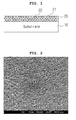
- FIG. 1 is a schematic cross-sectional view of a transparent CNT electrode according to an embodiment.
- the transparent CNT electrode of the present invention comprises a transparent substrate 10 and a CNT thin film 20 disposed on a surface of transparent substrate 10, wherein the CNT thin film contains CNTs 21 and a doped dispersant 22.
- the transparent substrate 10 used in the transparent CNT electrode can be of any type so long as it is transparent, specific examples of which include transparent inorganic substrates, such as glass and quartz substrates, and flexible transparent substrates, such as plastic substrates.
- suitable materials for the flexible transparent substrates include polyethylene terephthalate, polyethylene naphthalate, polyethylene sulfone, polycarbonate, polystyrene, polypropylene, polyester, polyimide, polyetheretherketone, polyetherimide, acrylic resins, olefin-maleimide copolymers, and norbornene resins. These materials can be used either alone or in a combination thereof.
- the CNTs 21 used in the CNT composition constituting the CNT thin film is not particularly restricted so long as the advantages of the present invention are not impaired.
- the CNTs 21 can be selected from the group consisting of single-walled carbon nanotubes, double-walled carbon nanotubes, multi-walled carbon nanotubes, rope carbon nanotubes, and combinations thereof. Where single-walled carbon nanotubes are desired for use, metallic carbon nanotubes can be selectively separated by a chemical separation process before use.
- the dispersant used to disperse the CNTs is not particularly restricted.
- the dispersant can be a conductive dispersant.
- the conductive dispersant can have a structure that consists of a head containing an aromatic ring with a high affinity for the CNTs and one tail or two tails that are the same or different, and with an affinity for the dispersion medium.
- the conductive dispersant can also be poly(3,4-ethylenedioxythiophene).
- the head of the dispersant is polythiophene.
- the dispersant exists in a doped state. Generally, the surface of the CNTs contained in the CNT thin film is surrounded by the dispersant. Since the dispersant has a lower conductivity than the CNTs, it functions as an insulator between the CNTs, resulting in a decrease in the total conductivity of the CNT thin film.
- the use of the doped dispersant in the transparent CNT electrode facilitates migration of the CNTs to achieve improved conductive properties of the CNT thin film.
- the mechanism responsible for the improvement in conductive properties will be explained in greater detail below.
- the conductive dispersant has the same composition as a conductive polymer. Depending on the dispersion medium and the CNTs used, the molecular weight of the conductive dispersant is controlled and one or two functional groups (which correspond to the tails of the dispersant) are introduced into the conductive dispersant.
- the conductive dispersant has basic characteristics similar to those of a conductive polymer. That is, a conductive polymer has a conjugated structure in which single bonds and double bonds are alternately repeated, and generally exhibits insulator (or semiconductor) properties. However, when a conductive polymer is chemically treated (i.e., is doped), its properties changed from insulator (or semiconductor) properties to conductor (or semiconductor) properties.
- This chemical treatment allows each bond between successive carbon atoms of the conductive polymer to have about one and a half bonds (i.e., a bond order of about 1.5) instead of single bonds (a bond order of 1) and double bonds (a bond order of 2) alternately repeated in the conjugated structure, so that the electron density of the conductive polymer is delocalized, thereby facilitating the intramolecular and intermolecular migration of electrons.
- the following Structural Formula 1 shows the states of polarons and bipolarons acting as charge carriers when a polythiophene polymer is doped.
- the type of dopant performing the above functions in the transparent CNT electrode of the present invention is not especially restricted.
- a p-type dopant (an electron acceptor) or an n-type dopant (an electron donor) can be used.
- Suitable p-type dopants include, but are not limited to, Lewis acids such as for example PF 5 , AsF 5 , SbF 5 , ClO 4 - , BF 4 , BF 3 , BCl 3 , BBr 3 , SO 3 , NO 2 (SbF 6 ), NO(SbCl 6 ), or NO 2 (BF 4 ); protic acids such as for example H 2 SO 4 , HClO 4 , HNO 3 , FSO 3 H, or CF 3 SO 3 H; transition metal halides such as for example FeCl 3 , MoCl 5 , WCl 5 , SnCl 4 , MoF 5 , RuF 5 , TaBr 5 and SnI 4 ; noble metal halides such as for example AuCl 3 and HAuCl 4 ; or organic materials such as for example benzoquinone, tetrachlorobenzoquinone, tetracyanoquinodimethane
- Lewis acids such
- n-type dopants include, but are not limited to, alkali metals such as for example Li, Na, K, or Cs, or alkylammonium ions such as for example tetraethylammonium ions or tetrabutylammonium ions.
- the CNTs and the dispersant may be mixed in a weight ratio of, but not limited to, 1 : 0.005 to 1 : 100. If the dispersant is used in an amount of less than the lower limit defined in the range, optimum dispersion effects of the CNTs cannot be attained. Meanwhile, if the dispersant is used in an amount exceeding the upper limit defined by the range, there is a possibility that the high conductivity of the CNTs may decrease, causing negative effects.
- the transmittance of the CNT thin film can be appropriately determined by those skilled in the art according to the intended applications and needs.
- the CNT transparent electrode using the doped dispersant exhibits excellent conductive properties, can be applied to various kinds of substrates, including flexible substrates, and is useful in a wide range of applications, for example, as a transparent electrode of a device, such as an image sensor, a solar cell, a liquid crystal display, an organic electroluminescence (“EL”) display or a touch screen panel.
- a transparent electrode of a device such as an image sensor, a solar cell, a liquid crystal display, an organic electroluminescence (“EL”) display or a touch screen panel.
- EL organic electroluminescence
- the transmittance of the structure comprising the CNT thin film and transparent substrate can also be appropriately determined by those skilled in the art according to the intended applications and needs.
- a visible light transmittance of the structure comprising the CNT thin film and transparent substrate of 60% or more, preferably 75% or more, at a wavelength of 550 nm or 600 nm, at a CNT film thickness of about 150 nm and a transparent substrate thickness of about 150 ⁇ m.
- the present invention is directed to a method for producing the transparent CNT electrode.
- the method comprises (a) preparing a CNT composition for the formation of a CNT thin film, (b) forming a CNT thin film containing a conductive dispersant on a surface of the transparent substrate using the CNT composition, and (c) doping the CNT thin film formed on the transparent substrate in a dopant solution to dope the conductive dispersant contained in the CNT thin film.
- a dispersant is dissolved in a dispersion medium selected from organic solvents, water, and mixtures thereof to prepare a dispersant solution.
- CNTs and the dispersant solution are used to prepare a CNT composition.
- Dispersion media that can be used to prepare the CNT composition include, but are not limited to, organic solvents, water, mixtures of two or more organic solvents, and mixtures of at least one polar organic solvent (e.g., hydroxyl-containing organic solvents) and water.
- organic solvent that is commonly used in the art may be used.
- suitable organic solvents include alcohols, ketones, glycols, glycol ethers, glycol ether acetates, acetates, and terpineols. These organic solvents can be used alone or in combination.
- the concentration of the dispersant in the dispersant solution can be in the range of about 0.000025% to about 50% by weight based on the total weight of dispersant and dispersant medium, and the CNTs are present in the CNT composition an amount of about 0.005% to about 1% by weight, based on the total weight of CNT and dispersant solution.
- Another solvent may be used to dilute the CNTs in the CNT composition depending on the mode of formation of a thin film.
- the CNT composition prepared in step (a) is used to form a CNT thin film containing the conductive dispersant on a surface of the transparent substrate.
- the formation of a CNT thin film on a surface of the transparent substrate may be achieved by depositing the CNT composition by a general coating technique, such as spin coating, spray coating, filtration, or bar coating.
- a suitable coating technique can be selected depending on the characteristics of the solution and intended applications.
- the surface of the transparent substrate can, prior to deposition of the CNT composition, be pretreated by a conventional process, such as for example, but not limited to, O 2 plasma treatment.
- the transmittance of the CNT thin film can be appropriately determined by those skilled in the art according to the intended applications and needs.
- the transmittance of the CNT thin film electrode structure comprising the CNT thin film and transparent substrate can be appropriately determined by those skilled in the art according to the intended applications and needs.
- the dispersant contained in the CNT thin film is doped using a dopant solution to increase the conductivity of the CNT thin film.
- the doping of the dispersant can be performed by a chemical process, such as a solution or vapor process.
- step (c) can include the sub-steps of i) doping the transparent substrate having the CNT thin film formed thereon in a dopant solution, ii) washing the dopant remaining in the CNT thin film, and iii) drying the doped CNT thin film.
- the doping can be achieved by a general doping technique, such as dipping, spin coating or spray.
- doping of the conductive dispersant by the solution process is achieved by dipping the CNT thin film in a dopant solution for a specified time, preferably about 10 minutes to about 24 hours, and washing the doped CNT thin film by a technique known in the art to remove the dopant remaining in the CNT thin film.
- the washing is performed by dipping the doped CNT thin film in a nitromethane solution for about 10 minutes to about 24 hours.
- the washed CNT thin film is dried by a common drying technique to complete the doping of the conductive dispersant.
- the drying is preferably performed at about 80°C for about 2 hours and at room temperature for about 6 hours, sequentially.
- the drying time and temperature can be appropriately adjusted and controlled depending on the solvent present in the dopant solution.
- step (c) in the vapor process, can be carried out by placing the transparent substrate having the CNT thin film formed thereon in a reactor, filling the reactor with a halogen gas selected from iodine (I 2 ), bromine (Br 2 ), chlorine (Cl 2 ), iodine monochloride (ICl), iodine trichloride (ICl 3 ) or iodine monobromide (IBr), and exposing the transparent substrate to the halogen gas for about one hour or more, but is not limited to this procedure.
- a halogen gas selected from iodine (I 2 ), bromine (Br 2 ), chlorine (Cl 2 ), iodine monochloride (ICl), iodine trichloride (ICl 3 ) or iodine monobromide (IBr)
- a conductive dispersant represented by Formula 3 20 mg was dissolved in 20 ml of water, and then 20 mg of purified SWCNTs (single-walled carbon nanotubes) synthesized by an Arc-discharge process (Grade ASP-100F, ILJIN Nanotech Co., Ltd.) was added to the solution.
- SWCNTs single-walled carbon nanotubes synthesized by an Arc-discharge process
- Z is selected from the group consisting of -H, -CH 3 , -OH, carboxylic acid and its salts, sulfonic acid and its salts, and phosphoric acid and its salts, and n is an integer.
- Z in Formula (3) is a sulfonic acid sodium salt group, to provide the exemplary conductive dispersant, as used herein, having Formula (4).
- the CNT composition thus prepared was subjected to filtration to form a CNT layer on a transparent polyester film as a transparent substrate, and dried at 60°C for 2 hours.
- the visible light transmittance of the resulting structure was measured to be 77% at 600 nm, at a CNT film thickness of 150 nm and a thickness of the transparent polyester substrate of 150 ⁇ m.
- the resulting structure was dipped in a 0.25 M nitromethane solution of 2,3-dichloro-5,6-dicyano-p-benzoquinone ("DDQ") as a dopant for 4 hours and washed in a nitromethane solution for 12 hours to remove the dopant remaining in the CNT thin film. Thereafter, the washed structure was dried at 80°C for 2 hours and at room temperature for 6 hours sequentially to produce a transparent CNT electrode.
- DDQ 2,3-dichloro-5,6-dicyano-p-benzoquinone
- a transparent CNT electrode was produced in the same manner as in step i) of Example 1, except that a 0.1 M nitromethane solution of gold trichloride (AuCl 3 ) was used as the dopant solution.
- the sheet resistance was measured for a transparent CNT electrode produced in the same manner as in step i) of Example 1 but without doping (i.e., before doping), and for the transparent CNT electrodes produced in Examples 1 and 2 after doping, and a comparison of the results are shown in Table 1.
- the surface of the transparent CNT electrode produced in Example 1 was observed by scanning electron microscopy (SEM) (FIG. 2).
- Example 2 111 13.59 a
- the CNT electrodes have a visible light transmittance of 77% measured at 600 nm and a CNT thin film thickness of 150 nm and a transparent polyester substrate thickness of 150 ⁇ m.
- the transmittance of the transparent electrode structure consisting of the CNT thin film and transparent substrate was measured using a UV-Visible spectrophotometer, at a CNT thin film thickness of 150 nm and a transparent substrate thickness of 150 ⁇ m.
- the sheet resistance ( ⁇ /sq.) of the transparent electrodes was determined using a four-point probe.
- the sheet resistance values of the transparent CNT electrodes measured after doping were reduced by an amount greater than about 50% and less than about 90% when compared with those of the transparent CNT electrodes measured before doping. From the results, it can be confirmed that when the transparent CNT electrodes are used as transparent electrodes of devices, such as image sensors, solar cells and liquid crystal displays, excellent characteristics of conductivity, transparency, and flexibility where desired can be imparted to the devices.
- Transparent CNT electrodes were produced in the same manner as in Example 1, except that CNT thin films were formed on respective PET films treated with O 2 plasma by spin coating.
- the transparent CNT electrodes thus produced had a visible light transmittance of 79.51% at 600 nm at a CNT thin film thickness of 150 nm and a PET film thickness of 150 ⁇ m.
- the transparent CNT electrodes were used to analyze effects according to the concentration of dopant solutions and the penetration time of dopants.
- nitromethane solutions having different concentrations (0.01 M and 0.1 M) of gold trichloride (AuCl 3 ) were used as dopant solutions, dipping was performed for different times (10 minutes, 20 minutes, one hour, and 4 hours), and washing was performed by rinsing with a nitromethane solution three times and dipping in the rinsing solution for one hour.
- the washed structures were dried overnight at room temperature.
- the transmittance and sheet resistance of the transparent CNT electrodes were measured by the procedure described in Example 1, and the results are shown in FIG. 4 and Table 2.
- Example 3 Five transparent CNT electrodes with different transmittance values were produced in the same manner as in Example 1, except that the contents of CNTs were varied, a 0.1 M nitromethane solution of gold trichloride (AuCl 3 ) was used as the dopant solution, and CNT thin films were formed on respective PET films treated with O 2 plasma by spin coating.
- the transparent CNT electrodes were used to analyze the doping effects with varying transmittance values.
- the transmittance (%T) and sheet resistance (Rs) of the transparent electrodes were measured by the procedure described in Example 1, and the results are shown in FIG. 5 and Table 3. TABLE 3 Sample No.
- Transmittance c (%) Sheet resistance ( ⁇ /sq.) Relative Sheet Resistance (Rs) value (% of before doping resistance) Before doping After doping 1 86.9 1291.62 855.8 66.6 2 85.7 933.59 739.1 55.2 3 81.6 650.34 536.8 69.7 4 75.8 555.17 311.2 35.0 5 74.5 387.49 272.3 77.9 c measured at 600 nm, a CNT thin film thickness of 150 nm and a transparent polyester substrate thickness of 150 ⁇ m.
- the sheet resistance values of the transparent CNT electrodes produced according to the above method decreased by an average of greater than 60% over the entire range of transmittance values, regardless of changes in the transmittance of the transparent electrode structures.
- the transparent CNT electrode of the present invention a doped dispersant is used to considerably increase the conductivity of a CNT thin film. Accordingly, the transparent CNT electrode of the present invention is useful in a wide range of applications, for example, as a transparent electrode of a device.
- the transparent CNT electrode of the present invention can be produced in a simple manner by a room temperature wet process without involving a sputtering process requiring expensive vacuum equipment, which is efficient in terms of production cost and processing, and exhibits excellent characteristics, such as high transmittance and low resistance.
- the transparent electrode of the present invention can be used as a flexible transparent electrode of a flexible display such as that currently in the spotlight as a next-generation display.
Landscapes
- Physics & Mathematics (AREA)
- Engineering & Computer Science (AREA)
- Chemical & Material Sciences (AREA)
- Spectroscopy & Molecular Physics (AREA)
- Nanotechnology (AREA)
- Crystallography & Structural Chemistry (AREA)
- Mathematical Physics (AREA)
- Theoretical Computer Science (AREA)
- Dispersion Chemistry (AREA)
- Manufacturing & Machinery (AREA)
- Nonlinear Science (AREA)
- General Physics & Mathematics (AREA)
- Optics & Photonics (AREA)
- Non-Insulated Conductors (AREA)
- Carbon And Carbon Compounds (AREA)
- Manufacturing Of Electric Cables (AREA)
Applications Claiming Priority (1)
| Application Number | Priority Date | Filing Date | Title |
|---|---|---|---|
| KR1020060100726A KR100790216B1 (ko) | 2006-10-17 | 2006-10-17 | 전도성 분산제를 이용한 cnt 투명전극 및 그의 제조방법 |
Publications (3)
| Publication Number | Publication Date |
|---|---|
| EP1914781A2 true EP1914781A2 (fr) | 2008-04-23 |
| EP1914781A3 EP1914781A3 (fr) | 2009-11-25 |
| EP1914781B1 EP1914781B1 (fr) | 2014-01-01 |
Family
ID=38857869
Family Applications (1)
| Application Number | Title | Priority Date | Filing Date |
|---|---|---|---|
| EP07116655.7A Ceased EP1914781B1 (fr) | 2006-10-17 | 2007-09-18 | Électrode transparente à nanotubes en carbone utilisant un dispersant conducteur et son procédé de fabrication |
Country Status (5)
| Country | Link |
|---|---|
| US (2) | US8138568B2 (fr) |
| EP (1) | EP1914781B1 (fr) |
| JP (1) | JP2008103329A (fr) |
| KR (1) | KR100790216B1 (fr) |
| CN (1) | CN101165883B (fr) |
Cited By (6)
| Publication number | Priority date | Publication date | Assignee | Title |
|---|---|---|---|---|
| WO2013026734A1 (fr) * | 2011-08-22 | 2013-02-28 | BSH Bosch und Siemens Hausgeräte GmbH | Appareil ménager à système de commande et d'affichage tactile |
| CN103764892A (zh) * | 2011-08-22 | 2014-04-30 | Bsh博世和西门子家用电器有限公司 | 带有接触敏感的操作和显示装置的家用设备 |
| EP2737496A4 (fr) * | 2011-07-28 | 2015-04-08 | Lg Innotek Co Ltd | Structure d'électrode et procédé de production d'électrode |
| DE102013223569A1 (de) | 2013-11-19 | 2015-05-21 | Fraunhofer-Gesellschaft zur Förderung der angewandten Forschung e.V. | Verfahren zur Herstellung einer homogenen leitfähigen Kohlenstoffnanoröhrchen haltigen Beschichtung auf einem Substrat und Substrat mit homogener leitfähiger Kohlenstoffnanoröhrchen haltiger Beschichtung |
| EP3421545A4 (fr) * | 2016-02-22 | 2020-03-11 | Sekisui Chemical Co., Ltd. | Matériau composite, matériau conducteur, particules conductrices et film conducteur |
| EP3671342A1 (fr) * | 2018-12-20 | 2020-06-24 | IMEC vzw | Stress induit pour la tension de pellicules uve |
Families Citing this family (125)
| Publication number | Priority date | Publication date | Assignee | Title |
|---|---|---|---|---|
| KR100790216B1 (ko) | 2006-10-17 | 2008-01-02 | 삼성전자주식회사 | 전도성 분산제를 이용한 cnt 투명전극 및 그의 제조방법 |
| KR100883737B1 (ko) * | 2007-01-17 | 2009-02-12 | 삼성전자주식회사 | 망상 탄소나노튜브 박막층을 포함하는 탄소나노튜브 투명전극 및 그의 제조방법 |
| KR100847987B1 (ko) * | 2007-02-27 | 2008-07-22 | 삼성전자주식회사 | 탄소나노튜브용 분산제 및 이를 포함하는 탄소나노튜브조성물 |
| CA2688335C (fr) | 2007-05-29 | 2015-07-21 | Innova Materials, Llc | Surfaces ayant des particules et procedes associes |
| KR100951730B1 (ko) * | 2007-05-30 | 2010-04-07 | 삼성전자주식회사 | 전도성이 개선된 카본나노튜브, 그의 제조방법 및 상기카본나노튜브를 함유하는 전극 |
| US8501529B2 (en) * | 2007-05-30 | 2013-08-06 | Samsung Electronics Co., Ltd. | Carbon nanotube having improved conductivity, process of preparing the same, and electrode comprising the carbon nanotube |
| KR100913700B1 (ko) * | 2007-06-12 | 2009-08-24 | 삼성전자주식회사 | 아민 화합물을 포함하는 탄소 나노튜브(cnt) 박막 및 그제조방법 |
| CN101470560B (zh) * | 2007-12-27 | 2012-01-25 | 清华大学 | 触摸屏及显示装置 |
| CN101419518B (zh) * | 2007-10-23 | 2012-06-20 | 清华大学 | 触摸屏 |
| CN101458603B (zh) * | 2007-12-12 | 2011-06-08 | 北京富纳特创新科技有限公司 | 触摸屏及显示装置 |
| CN101676832B (zh) * | 2008-09-19 | 2012-03-28 | 清华大学 | 台式电脑 |
| CN101458595B (zh) * | 2007-12-12 | 2011-06-08 | 清华大学 | 触摸屏及显示装置 |
| CN101470559B (zh) * | 2007-12-27 | 2012-11-21 | 清华大学 | 触摸屏及显示装置 |
| CN101458593B (zh) * | 2007-12-12 | 2012-03-14 | 清华大学 | 触摸屏及显示装置 |
| CN101458597B (zh) * | 2007-12-14 | 2011-06-08 | 清华大学 | 触摸屏、触摸屏的制备方法及使用该触摸屏的显示装置 |
| CN101458600B (zh) * | 2007-12-14 | 2011-11-30 | 清华大学 | 触摸屏及显示装置 |
| CN101458608B (zh) * | 2007-12-14 | 2011-09-28 | 清华大学 | 触摸屏的制备方法 |
| CN101470558B (zh) * | 2007-12-27 | 2012-11-21 | 清华大学 | 触摸屏及显示装置 |
| CN101458599B (zh) * | 2007-12-14 | 2011-06-08 | 清华大学 | 触摸屏、触摸屏的制备方法及使用该触摸屏的显示装置 |
| CN101458596B (zh) * | 2007-12-12 | 2011-06-08 | 北京富纳特创新科技有限公司 | 触摸屏及显示装置 |
| CN101458606B (zh) * | 2007-12-12 | 2012-06-20 | 清华大学 | 触摸屏、触摸屏的制备方法及使用该触摸屏的显示装置 |
| CN101458602B (zh) * | 2007-12-12 | 2011-12-21 | 清华大学 | 触摸屏及显示装置 |
| CN101620454A (zh) * | 2008-07-04 | 2010-01-06 | 清华大学 | 便携式电脑 |
| CN101458609B (zh) * | 2007-12-14 | 2011-11-09 | 清华大学 | 触摸屏及显示装置 |
| CN101458594B (zh) * | 2007-12-12 | 2012-07-18 | 清华大学 | 触摸屏及显示装置 |
| CN101458598B (zh) * | 2007-12-14 | 2011-06-08 | 清华大学 | 触摸屏及显示装置 |
| CN101458604B (zh) * | 2007-12-12 | 2012-03-28 | 清华大学 | 触摸屏及显示装置 |
| CN101656769B (zh) * | 2008-08-22 | 2012-10-10 | 清华大学 | 移动电话 |
| CN101419519B (zh) * | 2007-10-23 | 2012-06-20 | 清华大学 | 触摸屏 |
| CN101655720B (zh) * | 2008-08-22 | 2012-07-18 | 清华大学 | 个人数字助理 |
| CN101458605B (zh) * | 2007-12-12 | 2011-03-30 | 鸿富锦精密工业(深圳)有限公司 | 触摸屏及显示装置 |
| CN101464763B (zh) * | 2007-12-21 | 2010-09-29 | 清华大学 | 触摸屏的制备方法 |
| CN101470566B (zh) * | 2007-12-27 | 2011-06-08 | 清华大学 | 触摸式控制装置 |
| KR101435999B1 (ko) * | 2007-12-07 | 2014-08-29 | 삼성전자주식회사 | 도펀트로 도핑된 산화그라펜의 환원물, 이를 포함하는 박막및 투명전극 |
| CN101458975B (zh) * | 2007-12-12 | 2012-05-16 | 清华大学 | 电子元件 |
| CN101458601B (zh) * | 2007-12-14 | 2012-03-14 | 清华大学 | 触摸屏及显示装置 |
| CN101464757A (zh) * | 2007-12-21 | 2009-06-24 | 清华大学 | 触摸屏及显示装置 |
| CN101458607B (zh) * | 2007-12-14 | 2010-12-29 | 清华大学 | 触摸屏及显示装置 |
| CN101470565B (zh) * | 2007-12-27 | 2011-08-24 | 清华大学 | 触摸屏及显示装置 |
| CN101464765B (zh) * | 2007-12-21 | 2011-01-05 | 鸿富锦精密工业(深圳)有限公司 | 触摸屏及显示装置 |
| US8574393B2 (en) | 2007-12-21 | 2013-11-05 | Tsinghua University | Method for making touch panel |
| CN101464766B (zh) * | 2007-12-21 | 2011-11-30 | 清华大学 | 触摸屏及显示装置 |
| CN101464764B (zh) * | 2007-12-21 | 2012-07-18 | 清华大学 | 触摸屏及显示装置 |
| KR101596372B1 (ko) * | 2008-02-15 | 2016-03-08 | 삼성디스플레이 주식회사 | 표시장치용 투명전극, 표시장치 및 표시장치의 제조방법 |
| US8308930B2 (en) * | 2008-03-04 | 2012-11-13 | Snu R&Db Foundation | Manufacturing carbon nanotube ropes |
| JP5266889B2 (ja) * | 2008-06-04 | 2013-08-21 | ソニー株式会社 | 光透過性導電体の製造方法 |
| KR101450591B1 (ko) * | 2008-06-05 | 2014-10-17 | 삼성전자주식회사 | 탄소나노튜브 엔 도핑 물질 및 방법, 이를 이용한 소자 |
| US8946848B2 (en) * | 2008-06-05 | 2015-02-03 | Omnivision Technologies, Inc. | Apparatus and method for image sensor with carbon nanotube based transparent conductive coating |
| WO2009152146A1 (fr) * | 2008-06-09 | 2009-12-17 | Unidym, Inc. | Processus de nanotube de carbone/couche de finition améliorés pour réaliser un conducteur de greffon |
| US8237677B2 (en) * | 2008-07-04 | 2012-08-07 | Tsinghua University | Liquid crystal display screen |
| US8390580B2 (en) * | 2008-07-09 | 2013-03-05 | Tsinghua University | Touch panel, liquid crystal display screen using the same, and methods for making the touch panel and the liquid crystal display screen |
| KR101533096B1 (ko) | 2008-08-11 | 2015-07-02 | 삼성디스플레이 주식회사 | 전기영동표시장치 |
| KR101091196B1 (ko) * | 2008-08-14 | 2011-12-09 | 한국전기연구원 | 탄소나노튜브가 코팅된 폴리카보네이트 투명전도성 필름 및이를 이용한 터치패널 |
| US8673258B2 (en) * | 2008-08-14 | 2014-03-18 | Snu R&Db Foundation | Enhanced carbon nanotube |
| US8357346B2 (en) * | 2008-08-20 | 2013-01-22 | Snu R&Db Foundation | Enhanced carbon nanotube wire |
| US20100045610A1 (en) * | 2008-08-20 | 2010-02-25 | Snu R&Db Foundation | Transparent conductive films |
| WO2010022353A1 (fr) | 2008-08-21 | 2010-02-25 | Innova Meterials, Llc | Surfaces et revêtements améliorés, et procédés associés |
| US8021640B2 (en) | 2008-08-26 | 2011-09-20 | Snu R&Db Foundation | Manufacturing carbon nanotube paper |
| US9574272B2 (en) * | 2008-09-02 | 2017-02-21 | Ramot At Tel-Aviv University Ltd | Metal nanowire thin-films |
| KR100989409B1 (ko) * | 2008-12-17 | 2010-10-25 | 한국생산기술연구원 | 다층구조 플렉시블 투명전극 및 그 제조방법 |
| TWI395710B (zh) * | 2009-01-06 | 2013-05-11 | Univ Tatung | 奈米碳管複合材料之製作方法 |
| US8272124B2 (en) * | 2009-04-03 | 2012-09-25 | Formfactor, Inc. | Anchoring carbon nanotube columns |
| KR101039156B1 (ko) * | 2009-04-30 | 2011-06-03 | 한양대학교 산학협력단 | 탄소나노튜브층을 포함하는 태양전지 |
| IT1394220B1 (it) * | 2009-05-15 | 2012-06-01 | Univ Padova | Procedimento per la produzione di un manufatto di materiale plastico flessibile e trasparente con bassa resistenza elettrica superficiale e manufatto di materiale plastico ottenuto con questo procedimento. |
| KR101598565B1 (ko) * | 2009-05-26 | 2016-03-02 | 삼성디스플레이 주식회사 | 탄소나노튜브 투명전극 및 그의 제조방법 |
| CN101924816B (zh) * | 2009-06-12 | 2013-03-20 | 清华大学 | 柔性手机 |
| US9786444B2 (en) * | 2009-06-25 | 2017-10-10 | Nokia Technologies Oy | Nano-structured flexible electrodes, and energy storage devices using the same |
| JP5432624B2 (ja) * | 2009-07-28 | 2014-03-05 | パナソニック株式会社 | 透明導電膜付き基材 |
| KR101047215B1 (ko) * | 2009-07-30 | 2011-07-06 | 정태승 | 주사전자현미경〔sem〕용 전도성 콜드 마운팅 시편의 제작방법 |
| US20110048508A1 (en) * | 2009-08-26 | 2011-03-03 | International Business Machines Corporation | Doping of Carbon Nanotube Films for the Fabrication of Transparent Electrodes |
| CN102005443B (zh) * | 2009-09-02 | 2014-02-19 | 鸿富锦精密工业(深圳)有限公司 | 发光二极管封装结构及其制造方法 |
| KR20110061909A (ko) * | 2009-12-02 | 2011-06-10 | 삼성전자주식회사 | 도펀트로 도핑된 그라펜 및 이를 이용한 소자 |
| US8604332B2 (en) * | 2010-03-04 | 2013-12-10 | Guardian Industries Corp. | Electronic devices including transparent conductive coatings including carbon nanotubes and nanowire composites, and methods of making the same |
| US8460747B2 (en) * | 2010-03-04 | 2013-06-11 | Guardian Industries Corp. | Large-area transparent conductive coatings including alloyed carbon nanotubes and nanowire composites, and methods of making the same |
| US8518472B2 (en) * | 2010-03-04 | 2013-08-27 | Guardian Industries Corp. | Large-area transparent conductive coatings including doped carbon nanotubes and nanowire composites, and methods of making the same |
| KR101307962B1 (ko) | 2010-03-19 | 2013-09-12 | 엘지디스플레이 주식회사 | 터치인식 횡전계형 액정표시장치 및 이의 제조 방법 |
| KR101298234B1 (ko) * | 2010-03-19 | 2013-08-22 | 엘지디스플레이 주식회사 | 터치인식 횡전계형 액정표시장치 및 이의 제조 방법 |
| KR20110126998A (ko) * | 2010-05-18 | 2011-11-24 | 삼성전자주식회사 | Cnt 조성물, cnt 막구조체, 액정표시장치, cnt 막구조체의 제조방법 및 액정표시장치의 제조방법 |
| FR2961625A1 (fr) | 2010-06-16 | 2011-12-23 | Arkema France | Procede de preparation de films transparents conducteurs a base de nanotubes de carbone |
| US20120015098A1 (en) * | 2010-07-14 | 2012-01-19 | Qian Cheng | Carbon nanotube based transparent conductive films and methods for preparing and patterning the same |
| JP5988974B2 (ja) | 2010-08-07 | 2016-09-07 | ティーピーケイ ホールディング カンパニー リミテッド | 表面埋込添加物を有する素子構成要素および関連製造方法 |
| JP5627390B2 (ja) | 2010-10-22 | 2014-11-19 | 株式会社東芝 | 光電変換素子およびその製造方法 |
| CN102061101A (zh) * | 2010-10-29 | 2011-05-18 | 清华大学 | 碳纳米管复合材料 |
| KR101272483B1 (ko) * | 2010-12-09 | 2013-06-10 | 한국과학기술원 | 탄소나노튜브와 전도성 고분자를 이용한 다층 구조의 투명 전도성 판재의 제조방법 |
| JP5948837B2 (ja) * | 2011-03-29 | 2016-07-06 | ソニー株式会社 | 固体撮像素子及び電子機器 |
| CN103460123B (zh) * | 2011-04-15 | 2016-02-10 | 3M创新有限公司 | 用于电子显示器的透明电极 |
| CN102208546A (zh) * | 2011-04-18 | 2011-10-05 | 电子科技大学 | 一种柔性光电子器件用基板及其制备方法 |
| CN102201548B (zh) * | 2011-04-18 | 2014-04-23 | 电子科技大学 | 一种柔性发光器件用基板及其制备方法 |
| CN102208558B (zh) * | 2011-04-18 | 2013-07-10 | 电子科技大学 | 一种柔性发光器件用基板及其制备方法 |
| CN102819337B (zh) * | 2011-06-09 | 2015-06-17 | 天津富纳源创科技有限公司 | 触摸屏面板的制备方法 |
| CN102819335A (zh) * | 2011-06-09 | 2012-12-12 | 天津富纳源创科技有限公司 | 触摸屏面板的制备方法 |
| HK1201633A1 (en) | 2011-08-24 | 2015-09-04 | 宸鸿科技控股有限公司 | Patterned transparent conductors and related manufacturing methods |
| US20130100390A1 (en) * | 2011-10-25 | 2013-04-25 | Yewen Wang | Liquid Crystal Substrate and Manufacturing Method thereof, and Liquid Crystal Display Device |
| US8808792B2 (en) * | 2012-01-17 | 2014-08-19 | Northrop Grumman Systems Corporation | Carbon nanotube conductor with enhanced electrical conductivity |
| CN104508758B (zh) | 2012-03-01 | 2018-08-07 | 雷蒙特亚特特拉维夫大学有限公司 | 导电纳米线膜 |
| US9199870B2 (en) | 2012-05-22 | 2015-12-01 | Corning Incorporated | Electrostatic method and apparatus to form low-particulate defect thin glass sheets |
| CN103455179A (zh) * | 2012-05-28 | 2013-12-18 | 东元奈米应材股份有限公司 | 触控面板的透明导电层的高解析度激光蚀刻方法 |
| CN103625043A (zh) * | 2012-08-24 | 2014-03-12 | 天津富纳源创科技有限公司 | 碳纳米管薄膜板的制造方法及碳纳米管薄膜板 |
| US20140302296A9 (en) * | 2012-09-24 | 2014-10-09 | C3Nano Inc. | Transparent conductive films with carbon nanotubes, inks to form the films and corresponding processes |
| JP5717706B2 (ja) * | 2012-09-27 | 2015-05-13 | 株式会社東芝 | 半導体装置及びその製造方法 |
| CN104849317B (zh) | 2014-02-18 | 2018-09-18 | 元太科技工业股份有限公司 | 半导体感测装置及制作方法 |
| JP6197235B2 (ja) | 2014-06-26 | 2017-09-20 | 国立大学法人 奈良先端科学技術大学院大学 | ナノ材料−ドーパント組成物複合体の製造方法、ナノ材料−ドーパント組成物複合体およびドーパント組成物 |
| EP3163639B1 (fr) | 2014-06-26 | 2021-03-17 | National University Corporation Nara Institute of Science and Technology | Utilisation d'une composition dopante pour modifier le coefficient de seebeck d'un nanomatériau |
| CN105321592B (zh) * | 2014-08-01 | 2017-03-22 | 广东阿格蕾雅光电材料有限公司 | 碳纳米管‑高分子层状复合透明柔性电极及其制备方法 |
| KR101675887B1 (ko) | 2014-09-15 | 2016-11-15 | 청주대학교 산학협력단 | 플렉서블 투명전극용 다층시트 및 그 제조방법 |
| US10392520B2 (en) | 2014-10-17 | 2019-08-27 | National Institute Of Advanced Industrial Science And Technology | Carbon nanotube composite film and method for producing said composite film |
| US9296614B1 (en) | 2014-11-12 | 2016-03-29 | Corning Incorporated | Substrate such as for use with carbon nanotubes |
| CN104599746B (zh) | 2015-01-27 | 2017-06-09 | 京东方科技集团股份有限公司 | 一种触控元件及其制备方法和触摸屏 |
| CN104576321A (zh) * | 2015-01-30 | 2015-04-29 | 京东方科技集团股份有限公司 | 一种电极结构、其制作方法、显示基板及显示装置 |
| CN104616838B (zh) * | 2015-02-10 | 2018-02-06 | 京东方科技集团股份有限公司 | 一种电子器件的制作方法及电子器件 |
| DE102015102553A1 (de) * | 2015-02-23 | 2016-08-25 | Technische Hochschule Nürnberg Georg Simon Ohm | Dispergier-Additiv |
| CN104731413B (zh) * | 2015-04-02 | 2018-11-23 | 京东方科技集团股份有限公司 | 触控单元及其制作方法和柔性触控显示装置 |
| CN104934551B (zh) * | 2015-05-14 | 2017-07-28 | 京东方科技集团股份有限公司 | 一种柔性电极层及其制备方法、显示基板、显示装置 |
| JP6390027B2 (ja) * | 2015-11-24 | 2018-09-19 | 矢崎総業株式会社 | カーボンナノチューブ複合材料 |
| JP6626708B2 (ja) * | 2015-12-18 | 2019-12-25 | 富士フイルム株式会社 | 分散組成物の製造方法および熱電変換層の製造方法 |
| CN109071228B (zh) * | 2016-03-24 | 2023-01-13 | 古河电气工业株式会社 | 碳纳米管复合体和碳纳米管线材 |
| EP3440904A4 (fr) | 2016-04-07 | 2019-12-11 | Technology Innovation Momentum Fund (Israel) Limited Partnership | Impression de films de nanofils |
| KR102351982B1 (ko) * | 2017-04-13 | 2022-01-17 | 광주과학기술원 | 도핑된 공액고분자 및 이를 포함하는 유기전계효과 트랜지스터 |
| JP6977571B2 (ja) * | 2018-01-12 | 2021-12-08 | コニカミノルタ株式会社 | 有機機能性薄膜、有機機能性積層膜、有機エレクトロルミネッセンス素子、光電変換素子及び有機機能性薄膜形成用塗布液 |
| CN110391341B (zh) * | 2018-04-16 | 2023-08-22 | 清华大学 | 聚合物太阳能电池的制备方法 |
| CN110120449B (zh) * | 2019-05-24 | 2020-12-22 | 广东省半导体产业技术研究院 | 一种透明柔性显示系统及其制备方法 |
| KR20230050055A (ko) | 2021-10-07 | 2023-04-14 | 동의대학교 산학협력단 | 투명 전도성 전극 |
| CN114132918B (zh) * | 2021-12-31 | 2023-10-20 | 西安交通大学 | 一种量产的高电导多壁碳纳米管薄膜材料的制备方法 |
| CN114195131A (zh) * | 2022-01-04 | 2022-03-18 | 大连工业大学 | 一种单壁碳纳米管透明电热膜及其制备方法 |
| KR102762721B1 (ko) | 2022-05-02 | 2025-02-04 | 동의대학교 산학협력단 | 금속층의 상변태를 이용한 반투명 면상 발열체의 제조방법 |
Citations (1)
| Publication number | Priority date | Publication date | Assignee | Title |
|---|---|---|---|---|
| TWI251354B (en) | 2005-02-02 | 2006-03-11 | Ind Tech Res Inst | Solar energy power module with carbon nano-tube |
Family Cites Families (30)
| Publication number | Priority date | Publication date | Assignee | Title |
|---|---|---|---|---|
| US4183620A (en) * | 1976-12-30 | 1980-01-15 | Pedro Buarque De Macedo | Joint doped porous glass article with high modifier concentrations |
| US4645713A (en) * | 1985-01-25 | 1987-02-24 | Agency Of Industrial Science & Technology | Method for forming conductive graphite film and film formed thereby |
| JPH05241165A (ja) | 1992-02-28 | 1993-09-21 | Matsushita Electric Ind Co Ltd | 液晶表示装置及びその製造方法 |
| US6066442A (en) | 1995-10-23 | 2000-05-23 | Konica Corporation | Plastic film having an improved anti-static property |
| EP1244168A1 (fr) * | 2001-03-20 | 2002-09-25 | Francois Sugnaux | Electrode à réseau mésoporeux pour batterie |
| US6872681B2 (en) | 2001-05-18 | 2005-03-29 | Hyperion Catalysis International, Inc. | Modification of nanotubes oxidation with peroxygen compounds |
| JP4207398B2 (ja) | 2001-05-21 | 2009-01-14 | 富士ゼロックス株式会社 | カーボンナノチューブ構造体の配線の製造方法、並びに、カーボンナノチューブ構造体の配線およびそれを用いたカーボンナノチューブデバイス |
| US7563711B1 (en) | 2001-07-25 | 2009-07-21 | Nantero, Inc. | Method of forming a carbon nanotube-based contact to semiconductor |
| AU2002357037A1 (en) * | 2001-11-30 | 2003-06-17 | The Trustees Of Boston College | Coated carbon nanotube array electrodes |
| EP1513621A4 (fr) | 2002-05-21 | 2005-07-06 | Eikos Inc | Procede de configuration de revetement de nanotubes de carbone et de cablage de nanotubes de carbone |
| US7261852B2 (en) | 2002-07-19 | 2007-08-28 | University Of Florida Research Foundation, Inc. | Transparent electrodes from single wall carbon nanotubes |
| KR100759547B1 (ko) * | 2002-07-29 | 2007-09-18 | 삼성에스디아이 주식회사 | 연료전지용 탄소나노튜브, 그 제조방법 및 이를 채용한연료전지 |
| US20040265550A1 (en) * | 2002-12-06 | 2004-12-30 | Glatkowski Paul J. | Optically transparent nanostructured electrical conductors |
| KR100551229B1 (ko) * | 2003-06-26 | 2006-02-10 | 주식회사 디피아이 솔루션스 | 디스플레이용 유기 투명 전극의 제조방법 |
| US7455793B2 (en) * | 2004-03-31 | 2008-11-25 | E.I. Du Pont De Nemours And Company | Non-aqueous dispersions comprising electrically doped conductive polymers and colloid-forming polymeric acids |
| US7378040B2 (en) | 2004-08-11 | 2008-05-27 | Eikos, Inc. | Method of forming fluoropolymer binders for carbon nanotube-based transparent conductive coatings |
| US7247670B2 (en) * | 2004-08-24 | 2007-07-24 | General Electric Company | Nanotubes and methods of dispersing and separating nanotubes |
| US7226818B2 (en) | 2004-10-15 | 2007-06-05 | General Electric Company | High performance field effect transistors comprising carbon nanotubes fabricated using solution based processing |
| JP2006171336A (ja) | 2004-12-15 | 2006-06-29 | Takiron Co Ltd | 画像表示用透明電極体および画像表示装置 |
| KR100675334B1 (ko) * | 2005-02-19 | 2007-01-29 | 한국기계연구원 | 탄소나노튜브 필름 및 그 제조 방법 |
| JP5023456B2 (ja) * | 2005-03-28 | 2012-09-12 | 大日本印刷株式会社 | 有機薄膜太陽電池素子 |
| US7710739B2 (en) * | 2005-04-28 | 2010-05-04 | Semiconductor Energy Laboratory Co., Ltd. | Semiconductor device and display device |
| US7645497B2 (en) | 2005-06-02 | 2010-01-12 | Eastman Kodak Company | Multi-layer conductor with carbon nanotubes |
| US7593004B2 (en) | 2005-06-02 | 2009-09-22 | Eastman Kodak Company | Touchscreen with conductive layer comprising carbon nanotubes |
| KR100754984B1 (ko) | 2005-11-16 | 2007-09-04 | 한국과학기술원 | 탄소나노튜브 분산액을 이용한 고순도 탄소나노튜브 필름의 제조방법 |
| KR20070076875A (ko) | 2006-01-20 | 2007-07-25 | 삼성전자주식회사 | 탄소나노튜브용 분산제 및 그를 포함하는 탄소나노튜브조성물 |
| JP5071921B2 (ja) * | 2006-06-08 | 2012-11-14 | 独立行政法人産業技術総合研究所 | スメクティック液晶化合物 |
| JP2008081384A (ja) | 2006-09-29 | 2008-04-10 | Fuji Xerox Co Ltd | カーボンナノチューブ分散液およびカーボンナノチューブ構造体の製造方法、並びにカーボンナノチューブ構造体 |
| KR100790216B1 (ko) | 2006-10-17 | 2008-01-02 | 삼성전자주식회사 | 전도성 분산제를 이용한 cnt 투명전극 및 그의 제조방법 |
| KR20090105761A (ko) | 2008-04-03 | 2009-10-07 | 삼성전자주식회사 | 탄소나노튜브 투명 전극 및 그 제조 방법 |
-
2006
- 2006-10-17 KR KR1020060100726A patent/KR100790216B1/ko not_active Expired - Fee Related
-
2007
- 2007-04-13 US US11/735,178 patent/US8138568B2/en not_active Expired - Fee Related
- 2007-09-18 EP EP07116655.7A patent/EP1914781B1/fr not_active Ceased
- 2007-10-15 JP JP2007268075A patent/JP2008103329A/ja active Pending
- 2007-10-16 CN CN2007101625077A patent/CN101165883B/zh not_active Expired - Fee Related
-
2012
- 2012-02-14 US US13/372,881 patent/US8603836B2/en active Active
Patent Citations (1)
| Publication number | Priority date | Publication date | Assignee | Title |
|---|---|---|---|---|
| TWI251354B (en) | 2005-02-02 | 2006-03-11 | Ind Tech Res Inst | Solar energy power module with carbon nano-tube |
Non-Patent Citations (1)
| Title |
|---|
| NANO LETTERS, vol. 5, no. 4, 2005, pages 757 - 760 |
Cited By (12)
| Publication number | Priority date | Publication date | Assignee | Title |
|---|---|---|---|---|
| EP2737496A4 (fr) * | 2011-07-28 | 2015-04-08 | Lg Innotek Co Ltd | Structure d'électrode et procédé de production d'électrode |
| US9754702B2 (en) | 2011-07-28 | 2017-09-05 | Lg Innotek Co., Ltd. | Electrode structure and method for producing electrode |
| WO2013026734A1 (fr) * | 2011-08-22 | 2013-02-28 | BSH Bosch und Siemens Hausgeräte GmbH | Appareil ménager à système de commande et d'affichage tactile |
| CN103748276A (zh) * | 2011-08-22 | 2014-04-23 | Bsh博世和西门子家用电器有限公司 | 带有接触敏感的操作和显示装置的家用设备 |
| CN103764892A (zh) * | 2011-08-22 | 2014-04-30 | Bsh博世和西门子家用电器有限公司 | 带有接触敏感的操作和显示装置的家用设备 |
| RU2586829C2 (ru) * | 2011-08-22 | 2016-06-10 | Бсх Хаусгерете Гмбх | Бытовой прибор с сенсорным устройством управления и индикации |
| RU2591144C2 (ru) * | 2011-08-22 | 2016-07-10 | Бсх Хаусгерете Гмбх | Бытовой прибор с сенсорным устройством управления и индикации |
| EP2748369B1 (fr) * | 2011-08-22 | 2021-11-10 | BSH Hausgeräte GmbH | Appareil ménager à système de commande et d'affichage tactile |
| DE102013223569A1 (de) | 2013-11-19 | 2015-05-21 | Fraunhofer-Gesellschaft zur Förderung der angewandten Forschung e.V. | Verfahren zur Herstellung einer homogenen leitfähigen Kohlenstoffnanoröhrchen haltigen Beschichtung auf einem Substrat und Substrat mit homogener leitfähiger Kohlenstoffnanoröhrchen haltiger Beschichtung |
| EP3421545A4 (fr) * | 2016-02-22 | 2020-03-11 | Sekisui Chemical Co., Ltd. | Matériau composite, matériau conducteur, particules conductrices et film conducteur |
| EP3671342A1 (fr) * | 2018-12-20 | 2020-06-24 | IMEC vzw | Stress induit pour la tension de pellicules uve |
| US11163229B2 (en) | 2018-12-20 | 2021-11-02 | Imec Vzw | Induced stress for EUV pellicle tensioning |
Also Published As
| Publication number | Publication date |
|---|---|
| KR100790216B1 (ko) | 2008-01-02 |
| US8603836B2 (en) | 2013-12-10 |
| CN101165883B (zh) | 2010-11-10 |
| JP2008103329A (ja) | 2008-05-01 |
| US8138568B2 (en) | 2012-03-20 |
| CN101165883A (zh) | 2008-04-23 |
| US20080088219A1 (en) | 2008-04-17 |
| EP1914781A3 (fr) | 2009-11-25 |
| US20120141666A1 (en) | 2012-06-07 |
| EP1914781B1 (fr) | 2014-01-01 |
Similar Documents
| Publication | Publication Date | Title |
|---|---|---|
| EP1914781B1 (fr) | Électrode transparente à nanotubes en carbone utilisant un dispersant conducteur et son procédé de fabrication | |
| Song et al. | Conductive channel formation for enhanced electrical conductivity of PEDOT: PSS with high work-function | |
| Yu et al. | Recent development of carbon nanotube transparent conductive films | |
| KR101435999B1 (ko) | 도펀트로 도핑된 산화그라펜의 환원물, 이를 포함하는 박막및 투명전극 | |
| Wang et al. | Ammonia-treated graphene oxide and PEDOT: PSS as hole transport layer for high-performance perovskite solar cells with enhanced stability | |
| CN103777417B (zh) | 复合透明导体及其形成方法 | |
| Zheng et al. | Carbon nano-onions as a functional dopant to modify hole transporting layers for improving stability and performance of planar perovskite solar cells | |
| KR101240276B1 (ko) | 설포닐 히드라지드 계열 환원제를 이용한 그래핀 박막 및 이를 이용한 광전소자의 제조방법 | |
| CN110429181B (zh) | 有机光电器件及其制备方法 | |
| US20080296683A1 (en) | Carbon nanotube having improved conductivity, process of preparing the same, and electrode comprising the carbon nanotube | |
| US8513804B2 (en) | Nanotube-based electrodes | |
| KR101479830B1 (ko) | 슈퍼커패시터용 그래핀/전도성 고분자 필름 및 이의 제조방법 | |
| Lukaszkowicz et al. | Graphene-based layers deposited onto flexible substrates: used in dye-sensitized solar cells as counter electrodes | |
| US20110048508A1 (en) | Doping of Carbon Nanotube Films for the Fabrication of Transparent Electrodes | |
| WO2011141717A1 (fr) | Dispositif comprenant un film d'oxyde de graphène | |
| Wang et al. | A rhodanine modified poly-triarylamine dye function as a hole transport layer for inverted perovskite solar cells | |
| US20130025662A1 (en) | Water Soluble Dopant for Carbon Films | |
| US11935668B2 (en) | Conductive material, and conductive film and solar cell using same | |
| KR101584222B1 (ko) | 그래핀 박막 이송 방법 및 이를 이용한 소자 | |
| KR20150042121A (ko) | 태양 전지 및 그 제조 방법 | |
| Bauld et al. | Solution processed graphene thin films and their applications in organic solar cells | |
| Yedikardeş et al. | Investigation of P3HT: WO3 hybrid electrochromic thin films prepared by solution blending doping | |
| KR20130114470A (ko) | 그래핀 박막 이송 방법 및 이를 이용한 소자 | |
| Ryu et al. | Transparent, conductive and flexible carbon nanotube films and their application in organic light emitting diodes | |
| EP3223328A1 (fr) | Cellule photovoltaïque organique et son procédé de fabrication |
Legal Events
| Date | Code | Title | Description |
|---|---|---|---|
| PUAI | Public reference made under article 153(3) epc to a published international application that has entered the european phase |
Free format text: ORIGINAL CODE: 0009012 |
|
| AK | Designated contracting states |
Kind code of ref document: A2 Designated state(s): AT BE BG CH CY CZ DE DK EE ES FI FR GB GR HU IE IS IT LI LT LU LV MC MT NL PL PT RO SE SI SK TR |
|
| AX | Request for extension of the european patent |
Extension state: AL BA HR MK RS |
|
| RIN1 | Information on inventor provided before grant (corrected) |
Inventor name: SHIN, HYEON JIN Inventor name: YI, DONG KEE Inventor name: YOON, SEON MI Inventor name: CHOI, JAE YOUNG Inventor name: CHOI, SEONG JAE |
|
| PUAL | Search report despatched |
Free format text: ORIGINAL CODE: 0009013 |
|
| RIC1 | Information provided on ipc code assigned before grant |
Ipc: H01J 9/02 20060101ALI20091012BHEP Ipc: C01B 31/02 20060101ALI20091012BHEP Ipc: H01J 1/304 20060101AFI20080108BHEP |
|
| AK | Designated contracting states |
Kind code of ref document: A3 Designated state(s): AT BE BG CH CY CZ DE DK EE ES FI FR GB GR HU IE IS IT LI LT LU LV MC MT NL PL PT RO SE SI SK TR |
|
| AX | Request for extension of the european patent |
Extension state: AL BA HR MK RS |
|
| 17P | Request for examination filed |
Effective date: 20100519 |
|
| 17Q | First examination report despatched |
Effective date: 20100618 |
|
| AKX | Designation fees paid |
Designated state(s): DE FR GB |
|
| RAP1 | Party data changed (applicant data changed or rights of an application transferred) |
Owner name: SAMSUNG ELECTRONICS CO., LTD. |
|
| GRAP | Despatch of communication of intention to grant a patent |
Free format text: ORIGINAL CODE: EPIDOSNIGR1 |
|
| INTG | Intention to grant announced |
Effective date: 20130830 |
|
| GRAS | Grant fee paid |
Free format text: ORIGINAL CODE: EPIDOSNIGR3 |
|
| GRAA | (expected) grant |
Free format text: ORIGINAL CODE: 0009210 |
|
| AK | Designated contracting states |
Kind code of ref document: B1 Designated state(s): DE FR GB |
|
| REG | Reference to a national code |
Ref country code: GB Ref legal event code: FG4D |
|
| REG | Reference to a national code |
Ref country code: DE Ref legal event code: R096 Ref document number: 602007034534 Country of ref document: DE Effective date: 20140220 |
|
| REG | Reference to a national code |
Ref country code: DE Ref legal event code: R097 Ref document number: 602007034534 Country of ref document: DE |
|
| PLBE | No opposition filed within time limit |
Free format text: ORIGINAL CODE: 0009261 |
|
| STAA | Information on the status of an ep patent application or granted ep patent |
Free format text: STATUS: NO OPPOSITION FILED WITHIN TIME LIMIT |
|
| 26N | No opposition filed |
Effective date: 20141002 |
|
| REG | Reference to a national code |
Ref country code: DE Ref legal event code: R097 Ref document number: 602007034534 Country of ref document: DE Effective date: 20141002 |
|
| REG | Reference to a national code |
Ref country code: FR Ref legal event code: PLFP Year of fee payment: 10 |
|
| REG | Reference to a national code |
Ref country code: FR Ref legal event code: PLFP Year of fee payment: 11 |
|
| REG | Reference to a national code |
Ref country code: FR Ref legal event code: PLFP Year of fee payment: 12 |
|
| PGFP | Annual fee paid to national office [announced via postgrant information from national office to epo] |
Ref country code: GB Payment date: 20220822 Year of fee payment: 16 Ref country code: DE Payment date: 20220615 Year of fee payment: 16 |
|
| PGFP | Annual fee paid to national office [announced via postgrant information from national office to epo] |
Ref country code: FR Payment date: 20220822 Year of fee payment: 16 |
|
| P01 | Opt-out of the competence of the unified patent court (upc) registered |
Effective date: 20230530 |
|
| REG | Reference to a national code |
Ref country code: DE Ref legal event code: R119 Ref document number: 602007034534 Country of ref document: DE |
|
| GBPC | Gb: european patent ceased through non-payment of renewal fee |
Effective date: 20230918 |
|
| PG25 | Lapsed in a contracting state [announced via postgrant information from national office to epo] |
Ref country code: GB Free format text: LAPSE BECAUSE OF NON-PAYMENT OF DUE FEES Effective date: 20230918 |
|
| PG25 | Lapsed in a contracting state [announced via postgrant information from national office to epo] |
Ref country code: GB Free format text: LAPSE BECAUSE OF NON-PAYMENT OF DUE FEES Effective date: 20230918 Ref country code: FR Free format text: LAPSE BECAUSE OF NON-PAYMENT OF DUE FEES Effective date: 20230930 Ref country code: DE Free format text: LAPSE BECAUSE OF NON-PAYMENT OF DUE FEES Effective date: 20240403 |