EP1914799A1 - Verfahren zum herstellen von silizium auf isolator - Google Patents
Verfahren zum herstellen von silizium auf isolator Download PDFInfo
- Publication number
- EP1914799A1 EP1914799A1 EP06775242A EP06775242A EP1914799A1 EP 1914799 A1 EP1914799 A1 EP 1914799A1 EP 06775242 A EP06775242 A EP 06775242A EP 06775242 A EP06775242 A EP 06775242A EP 1914799 A1 EP1914799 A1 EP 1914799A1
- Authority
- EP
- European Patent Office
- Prior art keywords
- wafer
- silicon
- layer
- soi
- insulator
- Prior art date
- Legal status (The legal status is an assumption and is not a legal conclusion. Google has not performed a legal analysis and makes no representation as to the accuracy of the status listed.)
- Ceased
Links
Images


Classifications
-
- H—ELECTRICITY
- H10—SEMICONDUCTOR DEVICES; ELECTRIC SOLID-STATE DEVICES NOT OTHERWISE PROVIDED FOR
- H10P—GENERIC PROCESSES OR APPARATUS FOR THE MANUFACTURE OR TREATMENT OF DEVICES COVERED BY CLASS H10
- H10P30/00—Ion implantation into wafers, substrates or parts of devices
- H10P30/20—Ion implantation into wafers, substrates or parts of devices into semiconductor materials, e.g. for doping
- H10P30/208—Ion implantation into wafers, substrates or parts of devices into semiconductor materials, e.g. for doping of electrically inactive species
- H10P30/209—Ion implantation into wafers, substrates or parts of devices into semiconductor materials, e.g. for doping of electrically inactive species in silicon to make buried insulating layers
-
- H—ELECTRICITY
- H10—SEMICONDUCTOR DEVICES; ELECTRIC SOLID-STATE DEVICES NOT OTHERWISE PROVIDED FOR
- H10P—GENERIC PROCESSES OR APPARATUS FOR THE MANUFACTURE OR TREATMENT OF DEVICES COVERED BY CLASS H10
- H10P30/00—Ion implantation into wafers, substrates or parts of devices
- H10P30/20—Ion implantation into wafers, substrates or parts of devices into semiconductor materials, e.g. for doping
- H10P30/202—Ion implantation into wafers, substrates or parts of devices into semiconductor materials, e.g. for doping characterised by the semiconductor materials
- H10P30/206—Ion implantation into wafers, substrates or parts of devices into semiconductor materials, e.g. for doping characterised by the semiconductor materials into Group III-V semiconductors
-
- H—ELECTRICITY
- H10—SEMICONDUCTOR DEVICES; ELECTRIC SOLID-STATE DEVICES NOT OTHERWISE PROVIDED FOR
- H10P—GENERIC PROCESSES OR APPARATUS FOR THE MANUFACTURE OR TREATMENT OF DEVICES COVERED BY CLASS H10
- H10P30/00—Ion implantation into wafers, substrates or parts of devices
- H10P30/20—Ion implantation into wafers, substrates or parts of devices into semiconductor materials, e.g. for doping
- H10P30/208—Ion implantation into wafers, substrates or parts of devices into semiconductor materials, e.g. for doping of electrically inactive species
-
- H—ELECTRICITY
- H10—SEMICONDUCTOR DEVICES; ELECTRIC SOLID-STATE DEVICES NOT OTHERWISE PROVIDED FOR
- H10P—GENERIC PROCESSES OR APPARATUS FOR THE MANUFACTURE OR TREATMENT OF DEVICES COVERED BY CLASS H10
- H10P90/00—Preparation of wafers not covered by a single main group of this subclass, e.g. wafer reinforcement
- H10P90/19—Preparing inhomogeneous wafers
- H10P90/1904—Preparing vertically inhomogeneous wafers
- H10P90/1906—Preparing SOI wafers
- H10P90/1922—Preparing SOI wafers using silicon etch back techniques, e.g. BESOI or ELTRAN
-
- H—ELECTRICITY
- H10—SEMICONDUCTOR DEVICES; ELECTRIC SOLID-STATE DEVICES NOT OTHERWISE PROVIDED FOR
- H10W—GENERIC PACKAGES, INTERCONNECTIONS, CONNECTORS OR OTHER CONSTRUCTIONAL DETAILS OF DEVICES COVERED BY CLASS H10
- H10W10/00—Isolation regions in semiconductor bodies between components of integrated devices
- H10W10/10—Isolation regions comprising dielectric materials
- H10W10/181—Semiconductor-on-insulator [SOI] isolation regions, e.g. buried oxide regions of SOI wafers
Definitions
- the invention relates to a process for manufacturing silicon-on-insulator, and more particularly, to a process for manufacturing silicon-on-insulator which combines ion implantation technology with bonding and thinning backside technology.
- Silicon-on-insulator(SOI) has been widely used in aeronautic and astronautical fields, military electronics, portable communication devices etc. due to its advantageous properties of high speed, low power and anti-radiation etc., and is considered as a technology of next generation silicon integrated circuit(IC), thereby attracting more attentions(see J.P.Colige, Silicon on Insulator Technology, Material of VLSI, Kulwer Academic Publiction 1991 ). With the fast development of automotive electronics IC, audio power amplifier IC and lighting devices etc., there is an increasing demand for power devices. The application of SOI substrates to power devices has arrested much attention due to its outstanding insulation property (see F. Udrea, D. Garner, K. Sheng, A.Popescu, H.T. Lim and W.I. Milne, SOI Power Devices, Electronics and communication Engineering Journal, Feb. 2000, p27 ).
- SIMOX Implanted Oxygen
- Bonding and Thinning backside technology are two of the mainstream SOI fabrication methods available nowadays.
- SIMOX an SOI structure is formed by implanting high dose oxygen ions into monocrystalline silicon wafers and forming a buried, insulating silicon dioxide (SiO 2 ) layer (BOX) after performing a high temperature annealing on the monocrystalline silicon wafers.
- Bonding and thinning backside technology an SOI structure is formed by bonding one thermally oxidized silicon wafer with a bare silicon wafer and then thinning a backside of the wafer to a desired thickness.
- oxygen ions with high energy (20-300KeV) and high dosage (10 17 -10 18 cm -2 ) are implanted into a silicon wafer, and a rich-oxygen area is generated at a certain depth in the silicon wafer and then a SiO 2 layer buried in the silicon wafer(i.e. BOX layer) is formed after performing a high temperature annealing.
- BOX layer a SiO 2 layer buried in the silicon wafer(i.e. BOX layer) is formed after performing a high temperature annealing.
- the adjustable thickness ranges of the BOX layer and a top silicon layer (active layer) are limited by the energy and dose of the implanted ions.
- the maximum thickness of BOX layer will not exceed 400nm while the maximum thickness of the top silicon layer is about 300nm.
- the BOX layer is formed by performing a high temperature annealing to facilitate the oxygen aggregation into nucleus, which makes the insulation property of the BOX layer inferior to that of SiO 2 layer formed by thermal oxidation.
- the bonding and thinning process involves bonding one silicon wafer with a surface covered by a thermal oxidation layer to another bare silicon wafer, and thinning the backside of the bonded silicon wafer to a desired thickness.
- the quality of BOX layer can be well controlled whereas the thickness of a top silicon layer (active layer) can hardly be controlled precisely.
- J.W. Neuner employed a plasma-aided chemical etching method to thin the top silicon layer, which achieved a top silicon layer with a thickness of 1um and an uniformity within ⁇ 0.1 ⁇ m (see J.W. Neuner, A.M.
- the France-based SOITEC proposed a new technology called Unibond.
- One of the key steps in this process involves forming a bubble layer by implanting hydrogen ions in a wafer. This bubble layer splits automatically during a subsequent annealing process, as a result of which the SOI uniformity as well as the thickness of the top silicon layer is precisely controlled prior to polishing which is determined by the uniform hydrogen ions implantation.
- the invention relates to a process for manufacturing silicon-on-insulator (SOI) wafers, which combines ion implantation process with bonding and thinning process and has the following advantages: the thickness of the top silicon layer is thin, and the uniformity of which can be well controlled by oxygen ion implantation, while the thickness of BOX layer can be adjusted in a large range feasibly by thermal oxidation process and the insulation property of which is good, thereby achieving a high quality SOI wafers with a feasible BOX layer thickness and a good uniformity of the top silicon layer.
- SOI silicon-on-insulator
- This invention comprises the following steps: First, forming a device wafer by an ion implantation process (In the case of requiring a thick top silicon layer, an epitaxial layer has to be grown on the implanted wafer or an epitaxial layer is grown on the top silicon layer upon completion of a final process. In these cases, the wafer is still called device wafer), bonding the device wafer (or device wafer with an oxidation layer) to a handle wafer (or an oxidation handle wafer), performing an annealing on the resultant wafer in an atmosphere of oxygen or water vapor to strengthen the bonding, then etching the device wafer by grinding and etching processes until the implanted layer (i.e.
- an etching stop layer is exposed, subsequently etching out the etching stop layer followed by performing a fine polishing or oxidation treatment on the top silicon layer, thereby forming a finished SOI wafer.
- the final thicknesses of the BOX layer and the top silicon layer are depended on the thicknesses of the oxidation layer and the implantation depth (or the thickness of the epitaxial layer) of the device wafer respectively.
- the method for manufacturing SOI wafers according to the invention includes the following steps:
- the above-mentioned semiconductor material can be one of silicon, gallium arsenide (GaAs), indium phosphide, and germanium(Ge).
- the aforesaid device wafer is fabricated by ion implantation process.
- the ion can be nitrogen(N) ion, oxygen(O) ion or other ions.
- the ions is selected in such a way that the ion layer implanted layer can act as an etching stop layer. O ion is preferred.
- the implantation energy of ions ranges from 10 KeV to 500 KeV, preferably from 70 KeV to 250 KeV, and the implantation dose of ions ranges from 1E15/cm 2 to 1E19/cm 2 , preferably from 5E16/cm 2 to 2E18/cm 2 .
- the implanted depth of ions ranges from 500 to 10000 angstroms( ⁇ ), and the ion implantation process may be performed at a constant temperature or a varying temperature, which ranges from 20 to 700°C .
- the aforesaid implantation can performed by using the well-established SIMOX implanter based on SIMOX process.
- the process conditions for the SIMOX process are as follows: the implantation energy of oxygen ions ranging from 30 KeV to 250 KeV, preferably from 70 KeV to 250 KeV, and the implantation dose of oxygen ions ranging from 5E16/cm 2 to 2E18/cm 2 preferably from 5E16/cm 2 to 7E17/cm 2 , an preferred implantation depth ranging 1000 to 5000 ⁇ and an implantation temperature ranging from 20 to 550°C.
- the aforesaid device wafer can be subjected to a subsequent treatment (including a high temperature annealing) for the purpose of making the interface of the implanted layer and non-implanted layer precipitous, which facilitates the stop of chemical etching at the interface.
- a subsequent treatment including a high temperature annealing
- the aforesaid subsequent high temperature annealing process can be performed at a temperature ranging from 600 to 1500°C, in a ramp up/down rate ranging from 0.5 to 10°C/minute under an atmosphere of mixed gases of oxygen and argon or oxygen and nitrogen, in which the oxygen concentration ranges from 0% to 100%.
- the aforesaid device wafer can not be subjected to the subsequent treatment, provided that the implantation dose is large and an etching stop layer can be formed against some particular chemical etching without a subsequent high temperature annealing.
- the aforesaid device wafer can be formed by performing a high temperature annealing on the implanted wafer followed by removing the surface SiO 2 layer or without removing the same; the SiO 2 layer formed by the high temperature annealing can be removed by using a commonly used dilute solution of HF in the art. If the SiO 2 layer is not removed, it will become a part of the buried SiO 2 layer of finished SOI wafer.
- the subsequent high temperature annealing can be performed at a temperature ranging from 1100°C to 1350°C , preferably in an atmosphere containing an oxygen concentration ranging from 0% to 60%.
- the aforesaid etching process may be a chemical etching or a plasma etching or any other method that enables etching stop at the ion implantation layer.
- the surface SiO 2 layer can be removed firstly and then an epitaxial layer can be grown to a certain thickness by an epitaxial method, i.e., an epitaxial layer is formed on the top silicon layer of the initial implanted wafer.
- the epitaxial process can be a conventional process commonly used in the semiconductor industry.
- the epitaxy can either be homogeneous or heterogenous.
- the epitaxial layer can be P- or N- type and can be doped with phosphor or boron or others dopants.
- the aforesaid insulation layer resulting from insulation treatment or oxidation treatment will serve as the buried layer of the final SOI wafers.
- the aforesaid insulation layer can be made of SiO 2 silicon nitride (Si 3 N 4 ) or other material that has insulation property.
- the insulation treatment can be carried out on the device wafer or the handle wafer or on both.
- the aforesaid insulation treatment refers to a method for growing insulation layer, such as an oxidation method for growing SiO 2 or a nitridation method for growing Si 3 N 4 .
- SiO 2 is usually used as an insulation layer, So the thus formed insulation layer acts as aburied layer of the final SOI wafer.
- the thickness of the buried SiO 2 layer ranges from 0.1 to 5 ⁇ m.
- the total thickness of the device wafer, the handle wafer and the buried SiO 2 layer is the thickness of the final SOI wafer.
- the aforesaid oxidation process can be a conventional process commonly used in IC industry, such as dry oxygen oxidation process or dry oxygen-wet oxygen-dry oxygen oxidation process.
- the aforesaid oxidized silicon can be grown on the device wafer or the handle wafer.
- SiO 2 layer is usually used as an insulation layer.
- the device wafer and the handle wafer are bonded by a bonding process.
- the bonding process can be performed by using the EVG bonding machine manufactured by EVG Group or using other types of bonding machines, and usually at room temperature.
- a plasma-assisted bonding process can be used for this purpose at room temperature.
- the aforesaid annealing can be performed in an atmosphere containing oxygen, which can be either dry oxygen, wet oxygen or a mixed gas.
- the aforesaid annealing can be performed at a temperature ranging from 200°C to 1400°C for a period from 0.5 hour to 15 hours.
- the aforesaid annealing can be performed at a temperature ranging from 1000°C to 1250°C for a period from 2 hours to 6 hours in a wet oxygen atmosphere.
- the aforesaid single side thinning can be performed by a grinder or other machines that enable a silicon wafer thinning.
- the thickness after thinning ranges from 1 ⁇ m to 100 ⁇ m, preferably from 3 ⁇ m to 30 ⁇ m.
- the etch selectivity ratio of material to be etched to the ion implanted layer should be large enough to make the etching stop at the ion implanted layer.
- the etchant used in the aforesaid etching process may include potassium hydroxide (KOH), Tetramethyl Ammonium Hydroxide (TMAH) or other chemicals that has large etch selectivity ratio of silicon to the ion implanted layer.
- KOH potassium hydroxide
- TMAH Tetramethyl Ammonium Hydroxide
- KOH solution or TMAH solution is selected as an etchant to etch silicon.
- the ratio of chemical (such as KOH or TMAH) to deionized water in the etchant is 1:1000, preferably from 1:1 to 1:100.
- etching it needs heating the etchant to a temperature ranging from 25°C to 200°C , preferably from 50°C to 150°C.
- the implanted layer can also be removed directly by a polishing method.
- the implanted layer can be removed by a chemical etchant selected appropriately. If the implanted layer is SiO 2 layer, HF solution can be selected as the chemical etchant.
- the ratio of solute to solvent ranges from 1:1 to 1:2000, preferably from 1:10 to 1:100.
- CMP Chemical Mechanical Polishing
- oxidation can be selected as a fine polishing process to adjust the thickness of the top silicon layer in the final SOI wafer and achieve a more smooth surface.
- the thickness of silicon layer removed by CMP ranges from 300 ⁇ to 5000 ⁇ , preferably from 300 ⁇ to 3000 ⁇ .
- the thickness of silicon layer removed by oxidation ranges from 300 ⁇ to 10000 ⁇ and preferably from 300 ⁇ to 5000 ⁇ .
- a top silicon layer in the nano scale can be achieved in the implanted wafer formed by an implantation process.
- the minimum thickness of the top silicon layer can be 30nm, and thickness uniformity is excellent with a thickness deviation of ⁇ 10nm.
- the thickness and uniformity can not be achieved by bonding and thinning process singly.
- the thickness of BOX layer in the SOI wafer can be adjusted in a wider range since it is produced by a thermal oxidation process.
- the BOX layer formed by a thermal oxidation process has good insulation property and an adjustable, uniform thickness (in a range of 0 ⁇ 5.0 ⁇ m), and the top silicon layer is a transplanted layer from an implanted wafer or an implanted wafer with an epitaxial layer.
- the etching stop layer of the implanted wafer ensures the thickness and uniformity of the top silicon layer prior to a final fine polishing (thickness uniformity is excellent with a thickness deviation of ⁇ 10nm), and therefore the final thickness deviation of the SOI wafer can be controlled within ⁇ 0.05um.
- the top silicon layer 16 has a 195.3 nanometers (nm) thickness and has an excellent uniformity with a thickness deviation of ⁇ 2.7nm.
- the buried layer is the sum of 14 plus 21, with a total thickness of 1000 ⁇ 10nm.
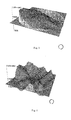
- the test data for uniformity of the top silicon layer 16 is shown in Fig. 3 .
- the epitaxial layer 18 has a 1.548 ⁇ m thickness and has an excellent uniformity with a thickness deviation of ⁇ 21.5nm.
- the buried layer is the sum of 17 plus 21, with a total thickness of 1000 ⁇ 10nm.
- the test data for uniformity of the epitaxial layer 18 is shown in Fig.4 .
Landscapes
- Element Separation (AREA)
Applications Claiming Priority (2)
| Application Number | Priority Date | Filing Date | Title |
|---|---|---|---|
| CNB2005100283656A CN100487885C (zh) | 2005-07-29 | 2005-07-29 | 一种绝缘体上硅的制作方法 |
| PCT/CN2006/001901 WO2007012290A1 (en) | 2005-07-29 | 2006-07-28 | Method for manufacturing silicon on insulator |
Publications (2)
| Publication Number | Publication Date |
|---|---|
| EP1914799A1 true EP1914799A1 (de) | 2008-04-23 |
| EP1914799A4 EP1914799A4 (de) | 2010-03-17 |
Family
ID=36139611
Family Applications (1)
| Application Number | Title | Priority Date | Filing Date |
|---|---|---|---|
| EP06775242A Ceased EP1914799A4 (de) | 2005-07-29 | 2006-07-28 | Verfahren zum herstellen von silizium auf isolator |
Country Status (3)
| Country | Link |
|---|---|
| EP (1) | EP1914799A4 (de) |
| CN (1) | CN100487885C (de) |
| WO (1) | WO2007012290A1 (de) |
Cited By (5)
| Publication number | Priority date | Publication date | Assignee | Title |
|---|---|---|---|---|
| EP2187429A4 (de) * | 2007-09-07 | 2011-03-02 | Sumco Corp | Bonding-wafer-herstellungsverfahren |
| US9136134B2 (en) | 2012-02-22 | 2015-09-15 | Soitec | Methods of providing thin layers of crystalline semiconductor material, and related structures and devices |
| US20160372424A1 (en) * | 2013-11-22 | 2016-12-22 | Shanghai Simgui Tehcnology Co., Ltd. | Low-warpage semiconductor substrate and method for preparing same |
| US20170018454A1 (en) * | 2013-11-22 | 2017-01-19 | Shanghai Simgui Tehcnology Co., Ltd. | Method for preparing low-warpage semiconductor substrate |
| US9673085B2 (en) | 2012-09-03 | 2017-06-06 | Shin-Etsu Handotai Co., Ltd. | Method for manufacturing SOI wafer |
Families Citing this family (17)
| Publication number | Priority date | Publication date | Assignee | Title |
|---|---|---|---|---|
| CN100454483C (zh) * | 2007-04-20 | 2009-01-21 | 中国电子科技集团公司第四十八研究所 | 一种离子注入厚膜soi晶片材料的制备方法 |
| CN100595882C (zh) * | 2007-12-28 | 2010-03-24 | 上海新傲科技股份有限公司 | 以键合减薄制备绝缘体上硅的方法 |
| US8324031B2 (en) | 2008-06-24 | 2012-12-04 | Globalfoundries Singapore Pte. Ltd. | Diffusion barrier and method of formation thereof |
| CN101532179B (zh) * | 2009-02-27 | 2011-04-20 | 中国电子科技集团公司第四十八研究所 | 绝缘体上硅晶片的制造方法 |
| CN101707188B (zh) * | 2009-11-27 | 2013-02-20 | 上海新傲科技股份有限公司 | 采用腐蚀工艺形成带有绝缘埋层的衬底的方法 |
| CN101908472B (zh) * | 2010-06-25 | 2015-10-14 | 上海新傲科技股份有限公司 | 在绝缘层中嵌入纳米晶的半导体材料制备方法 |
| JP5752264B2 (ja) | 2010-12-27 | 2015-07-22 | シャンハイ シングイ テクノロジー カンパニー リミテッドShanghai Simgui Technology Co., Ltd | 不純物のゲッタリングプロセスで絶縁層付きの半導体基板を製造する方法 |
| CN102130039B (zh) * | 2010-12-27 | 2013-04-10 | 上海新傲科技股份有限公司 | 采用吸杂工艺制备带有绝缘埋层的半导体衬底的方法 |
| CN102903607A (zh) * | 2011-06-30 | 2013-01-30 | 上海新傲科技股份有限公司 | 采用选择性腐蚀制备带有绝缘埋层的衬底的制备方法 |
| CN102515087A (zh) * | 2011-12-01 | 2012-06-27 | 上海先进半导体制造股份有限公司 | 流量传感器的制造方法 |
| CN102491260A (zh) * | 2011-12-31 | 2012-06-13 | 上海先进半导体制造股份有限公司 | 采用腐蚀自停止方式制造流量传感器的方法 |
| CN103367230B (zh) * | 2012-04-09 | 2016-05-25 | 中芯国际集成电路制造(上海)有限公司 | 超薄绝缘体上硅结构的制作方法、半导体器件的制作方法 |
| CN103077885B (zh) * | 2013-01-31 | 2016-06-01 | 上海新傲科技股份有限公司 | 受控减薄方法以及半导体衬底 |
| CN110085549B (zh) * | 2018-01-26 | 2021-06-04 | 沈阳硅基科技有限公司 | 一种双面注入得到soi的方法 |
| CN112490113A (zh) * | 2020-11-12 | 2021-03-12 | 武汉新芯集成电路制造有限公司 | 一种半导体器件的制作方法 |
| CN114696216B (zh) * | 2020-12-30 | 2025-11-07 | 山东华光光电子股份有限公司 | 一种可精确控制高度的半导体激光器垂直脊型结构的制作方法 |
| CN116053192B (zh) * | 2022-12-21 | 2024-02-09 | 中环领先半导体科技股份有限公司 | 一种半导体材料、制备方法和半导体器件 |
Family Cites Families (17)
| Publication number | Priority date | Publication date | Assignee | Title |
|---|---|---|---|---|
| JPH021914A (ja) * | 1988-06-10 | 1990-01-08 | Sony Corp | 半導体基板の製法 |
| JPH02228061A (ja) * | 1989-03-01 | 1990-09-11 | Nippon Telegr & Teleph Corp <Ntt> | Soi基板の製造方法 |
| JPH04115511A (ja) * | 1990-09-05 | 1992-04-16 | Fujitsu Ltd | Soi基板の製造方法 |
| JPH04206766A (ja) * | 1990-11-30 | 1992-07-28 | Hitachi Ltd | 半導体装置の製造方法 |
| JPH05129258A (ja) * | 1991-11-01 | 1993-05-25 | Hitachi Ltd | 半導体ウエハの製造方法および半導体集積回路装置の製造方法 |
| DE4210859C1 (de) * | 1992-04-01 | 1993-06-09 | Fraunhofer-Gesellschaft Zur Foerderung Der Angewandten Forschung Ev, 8000 Muenchen, De | |
| US5376579A (en) * | 1993-07-02 | 1994-12-27 | The United States Of America As Represented By The Secretary Of The Air Force | Schemes to form silicon-on-diamond structure |
| WO1998042010A1 (en) * | 1997-03-17 | 1998-09-24 | Genus, Inc. | Bonded soi wafers using high energy implant |
| US5981400A (en) * | 1997-09-18 | 1999-11-09 | Cornell Research Foundation, Inc. | Compliant universal substrate for epitaxial growth |
| JP3324469B2 (ja) * | 1997-09-26 | 2002-09-17 | 信越半導体株式会社 | Soiウエーハの製造方法ならびにこの方法で製造されるsoiウエーハ |
| US5930643A (en) * | 1997-12-22 | 1999-07-27 | International Business Machines Corporation | Defect induced buried oxide (DIBOX) for throughput SOI |
| JP3211233B2 (ja) * | 1998-08-31 | 2001-09-25 | 日本電気株式会社 | Soi基板及びその製造方法 |
| US6541356B2 (en) * | 2001-05-21 | 2003-04-01 | International Business Machines Corporation | Ultimate SIMOX |
| WO2004010505A1 (ja) * | 2002-07-18 | 2004-01-29 | Shin-Etsu Handotai Co.,Ltd. | Soiウェーハおよびその製造方法 |
| US6835633B2 (en) * | 2002-07-24 | 2004-12-28 | International Business Machines Corporation | SOI wafers with 30-100 Å buried oxide (BOX) created by wafer bonding using 30-100 Å thin oxide as bonding layer |
| FR2855908B1 (fr) * | 2003-06-06 | 2005-08-26 | Soitec Silicon On Insulator | Procede d'obtention d'une structure comprenant au moins un substrat et une couche ultramince |
| EP1710836A4 (de) * | 2004-01-30 | 2010-08-18 | Sumco Corp | Verfahren zur herstellung eines soi-wafers |
-
2005
- 2005-07-29 CN CNB2005100283656A patent/CN100487885C/zh not_active Expired - Lifetime
-
2006
- 2006-07-28 EP EP06775242A patent/EP1914799A4/de not_active Ceased
- 2006-07-28 WO PCT/CN2006/001901 patent/WO2007012290A1/zh not_active Ceased
Cited By (5)
| Publication number | Priority date | Publication date | Assignee | Title |
|---|---|---|---|---|
| EP2187429A4 (de) * | 2007-09-07 | 2011-03-02 | Sumco Corp | Bonding-wafer-herstellungsverfahren |
| US9136134B2 (en) | 2012-02-22 | 2015-09-15 | Soitec | Methods of providing thin layers of crystalline semiconductor material, and related structures and devices |
| US9673085B2 (en) | 2012-09-03 | 2017-06-06 | Shin-Etsu Handotai Co., Ltd. | Method for manufacturing SOI wafer |
| US20160372424A1 (en) * | 2013-11-22 | 2016-12-22 | Shanghai Simgui Tehcnology Co., Ltd. | Low-warpage semiconductor substrate and method for preparing same |
| US20170018454A1 (en) * | 2013-11-22 | 2017-01-19 | Shanghai Simgui Tehcnology Co., Ltd. | Method for preparing low-warpage semiconductor substrate |
Also Published As
| Publication number | Publication date |
|---|---|
| CN100487885C (zh) | 2009-05-13 |
| CN1744298A (zh) | 2006-03-08 |
| WO2007012290A1 (en) | 2007-02-01 |
| EP1914799A4 (de) | 2010-03-17 |
Similar Documents
| Publication | Publication Date | Title |
|---|---|---|
| EP1914799A1 (de) | Verfahren zum herstellen von silizium auf isolator | |
| US5213986A (en) | Process for making thin film silicon-on-insulator wafers employing wafer bonding and wafer thinning | |
| US6100165A (en) | Method of manufacturing semiconductor article | |
| US6054363A (en) | Method of manufacturing semiconductor article | |
| JP3265493B2 (ja) | Soi基板の製造方法 | |
| US6350702B2 (en) | Fabrication process of semiconductor substrate | |
| US6573126B2 (en) | Process for producing semiconductor article using graded epitaxial growth | |
| WO2004021420A2 (en) | Fabrication method for a monocrystalline semiconductor layer on a substrate | |
| CN110352484A (zh) | 高电阻率绝缘体上硅结构及其制造方法 | |
| CN113889432B (zh) | 绝缘体上半导体结构的制造方法 | |
| EP0843346B1 (de) | Verfahren zur Herstellung eines Halbleitergegenstands | |
| JP2001168308A (ja) | シリコン薄膜の製造方法、soi基板の作製方法及び半導体装置 | |
| JP2901031B2 (ja) | 半導体基材及びその作製方法 | |
| CN101286442A (zh) | Soi基板的制造方法 | |
| US7695564B1 (en) | Thermal management substrate | |
| TWI884271B (zh) | 用於製作射頻應用之絕緣體上半導體底材之方法 | |
| JPH04346418A (ja) | 半導体基材の作製方法 | |
| JP3347354B2 (ja) | エッチング方法および半導体基材の作製方法 | |
| US20020094678A1 (en) | Process for fabricating a single-crystal substrate and integrated circuit comprising such a substrate | |
| JP3112100B2 (ja) | 半導体基材の作製方法 | |
| JP3112101B2 (ja) | 半導体基材の作製方法 | |
| JPH09213916A (ja) | Soi基板の製造方法 | |
| JP3128076B2 (ja) | バイポーラトランジスタの製造方法及びそれを用いた半導体装置の製造方法 | |
| JPH0541488A (ja) | 半導体装置 | |
| JP3098811B2 (ja) | 絶縁ゲート型電界効果トランジスタ及びそれを用いた半導体装置 |
Legal Events
| Date | Code | Title | Description |
|---|---|---|---|
| PUAI | Public reference made under article 153(3) epc to a published international application that has entered the european phase |
Free format text: ORIGINAL CODE: 0009012 |
|
| 17P | Request for examination filed |
Effective date: 20080229 |
|
| AK | Designated contracting states |
Kind code of ref document: A1 Designated state(s): DE FR NL |
|
| RBV | Designated contracting states (corrected) |
Designated state(s): DE FR NL |
|
| A4 | Supplementary search report drawn up and despatched |
Effective date: 20100215 |
|
| 17Q | First examination report despatched |
Effective date: 20100422 |
|
| DAX | Request for extension of the european patent (deleted) | ||
| REG | Reference to a national code |
Ref country code: DE Ref legal event code: R003 |
|
| STAA | Information on the status of an ep patent application or granted ep patent |
Free format text: STATUS: THE APPLICATION HAS BEEN REFUSED |
|
| 18R | Application refused |
Effective date: 20130418 |