EP1916546A2 - Speicher mit integrierter Schaltung sowie Zugriffsvorrichtung und Gültigkeitsprüfverfahren für die Verwendung des Speichers mit integrierter Schaltung - Google Patents
Speicher mit integrierter Schaltung sowie Zugriffsvorrichtung und Gültigkeitsprüfverfahren für die Verwendung des Speichers mit integrierter Schaltung Download PDFInfo
- Publication number
- EP1916546A2 EP1916546A2 EP07252994A EP07252994A EP1916546A2 EP 1916546 A2 EP1916546 A2 EP 1916546A2 EP 07252994 A EP07252994 A EP 07252994A EP 07252994 A EP07252994 A EP 07252994A EP 1916546 A2 EP1916546 A2 EP 1916546A2
- Authority
- EP
- European Patent Office
- Prior art keywords
- memory
- data
- readout
- exclusive use
- specific information
- Prior art date
- Legal status (The legal status is an assumption and is not a legal conclusion. Google has not performed a legal analysis and makes no representation as to the accuracy of the status listed.)
- Withdrawn
Links
Images


Classifications
-
- G—PHYSICS
- G06—COMPUTING OR CALCULATING; COUNTING
- G06F—ELECTRIC DIGITAL DATA PROCESSING
- G06F21/00—Security arrangements for protecting computers, components thereof, programs or data against unauthorised activity
- G06F21/70—Protecting specific internal or peripheral components, in which the protection of a component leads to protection of the entire computer
- G06F21/78—Protecting specific internal or peripheral components, in which the protection of a component leads to protection of the entire computer to assure secure storage of data
- G06F21/79—Protecting specific internal or peripheral components, in which the protection of a component leads to protection of the entire computer to assure secure storage of data in semiconductor storage media, e.g. directly-addressable memories
Definitions
- the present invention relates to an IC memory having a plural number of memory portions therein, such as, a RFIF (Radio Frequency IdentI/Fication) tag, for example, representatively, and it also relates to a technology for accessing and/or controlling such the IC memory, etc.
- a RFIF Radio Frequency IdentI/Fication
- the RFIF tags there are various specifications made for fitting with various ways of using thereof, up to recent years, but as a standard, in particular, for the RFIF tag of UHF band, which is aimed for use, mainly in a business world of distribution, for example, the RFIF tag, in accordance with ISO/IEC 18000-6 Type C, it is able to have a plural number of rewritable memory portions, each of which is called "bank", and ID data of the RFID can be stored in a UII bank.
- TID bank can be stored information of a maker who manufactures the tag.
- RESERVED bank can be stored password data.
- each of users can store data, freely. Also, each of the banks can be made impossible to rewrite, eternally, with an aid of a password (Non-Patent Document 1).
- Non-Patent Document 1 ISO/IEC 18000-6:2004 Information technology - Radio frequency identI/Fication for item management - Part 6: Parameters for air inteRFace communications at 860 MHz to 960 MHz.
- an object of the present invention is to provide an IC memory, such as, the RFID tag, for example, for making the data thereof difficult to be reproduced or duplicated, but having ill influences upon the existing specification thereof.
- Another object of the present is to provide an IC memory, such as, the RFID tag, for example, for enabling to detect it easily, in particular, when the data thereof is reproduced or duplicated.
- an IC memory comprising: a plural number of data memory portions; an antenna, which is configured to conduct transmission of radio waves between an external communication apparatus; a signal process portion, which is configured to conduct modulation/demodulation process upon a signal received on said antenna; and a protocol process portion, which is configured to conduct protocol processing, including transmitting command and data, which are presented by said signal, to said external communication apparatus, writing data into said data memory portion, and managing an internal condition of said IC memory, wherein at least one of said data memory portion is a memory portion for exclusive use of readout, from which data is read out, and other data memory portions than said memory portion for exclusive use of readout are memory portions, on which any one of readout and write-in of data can be made.
- said memory portion for exclusive use of readout is a memory portion, into which the data is written at a fist change after being manufactured or when being manufactured, and after writing mentioned above, the data can be read out only.
- said protocol process portion comprises: a data readout enabling/disenabling setout portion, which is configured to determine an access setup, in relation to enabling/disenabling of readout or write-in, upon the other data memory portions of said memory portion for exclusive use of readout; and an access control portion, which is configured to control the readout and the write-in of said other data memory portions of said memory portion for exclusive use of readout, after determining said access setup, and said memory portion for exclusive use of readout is able to do only readout.
- a data readout enabling/disenabling setout portion which is configured to determine an access setup, in relation to enabling/disenabling of readout or write-in, upon the other data memory portions of said memory portion for exclusive use of readout
- an access control portion which is configured to control the readout and the write-in of said other data memory portions of said memory portion for exclusive use of readout, after determining said access setup, and said memory portion for exclusive use of readout is able to do only readout.
- said specific information stored within said memory portion for exclusive use of readout has a one value selected from the following values A-D:
- said specific information stored within said memory portion for exclusive use of readout includes group identification information for identifying to be different from other IC memory groups, which is assigned to a one IC memory group selected from a predetermined number of IC memory groups, and an individual number, which is assigned to said IC memory within said IC memory group selected, and said individual number has a one value selected from the following values A-D:
- calculation result data obtained by conducting a predetermined function calculation upon said specific information.
- calculation result data obtained by conducting a predetermined function calculation upon data, including said specific information and a part of the data stored in the other data memory portions.
- said calculation result data is made from cryptography calculation with using a common key or a public key.
- said calculation result data is calculated, but without using the function calculation.
- said IC memory is RFID, and has a RESERVED bank, a UII bank, a TID bank, and a USER bank, as the other data memory portions of said memory portion for exclusive use of readout, and said calculation result data is stored within said USER bank.
- a readout command to said memory portion for exclusive use of readout, to which said protocol process portion can respond is different from a readout command to the other memory portion, in command code thereof.
- a process is conducted on different protocol, for said external communication apparatus in cases when conducting an readout operation of said memory portion for exclusive use of readout, and when conducting readout and write-in operations onto the other memory portions.
- an external communication apparatus for conducting communication with the IC memory as described in the first aspect mentioned above, comprising: an antenna, which is configured to conduct transmission of radio waves between said IC memory; a signal process portion, which is configured to conduct modulation/demodulation process upon a signal received on said antenna; a protocol process portion, which is configured to conduct processing on a protocol of an external communication apparatus, transmitting command and data, which are presented by said signal, between said IC memory; and a calculate portion, which is configured to calculate out calculation result data through a predetermined function calculation, wherein said external communication apparatus protocol process portion comprises: a portion, which is configured to read out data from said memory portion for exclusive use of readout within said IC memory; a portion, which is configured to deliver the data, being read out from said memory portion for exclusive use of readout, as said calculation target data to said calculate portion, and to receive the calculation result data, being calculated out by said calculate portion upon basis of said readout data; and a portion, which is configured to write said
- an external communication apparatus for conducting communication with the IC memory as described in the first aspect mentioned above, comprising: an antenna, which is configured to conduct transmission of radio waves between said IC memory; a signal process portion, which is configured to conduct modulation/demodulation process upon a signal received on said antenna; a protocol process portion, which is configured to conduct processing on a protocol of an external communication apparatus, transmitting command and data, which are presented by said signal, between said IC memory; and a calculate portion, which is configured to calculate out calculation result data through a predetermined function calculation, wherein said external communication apparatus protocol process portion comprises: a portion, which is configured to readout data from said memory portion for exclusive use of readout within said IC memory; a portion, which is configured to deliver the data, being read out from said memory portion for exclusive use of readout, as said calculation target data to said calculate portion, and to receive the calculation result data, being calculated out by said calculate portion upon basis of said readout data; a portion , which is configured to read out data
- a process is conducted on different protocol, for said IC memory, in case where a readout command to said memory portion for exclusive use of readout, which said external communication apparatus protocol process portion transmits to said IC memory, is different from a readout command to the other memory portion, or when said external communication apparatus protocol process portion conducts the readout process of said memory portion for exclusive use of readout, or when it conducts the readout process or the write-in process of said other data memory portion.
- a system according to a fourth aspect of the present invention, comprises an IC memory according to the first aspect mentioned above, and an external communication apparatus, according to the second or the third aspect mentioned above.
- a system according to a fifth aspect of the present invention, comprises an IC memory according to the first aspect mentioned above, an external communication apparatus according to the second embodiment mentioned above, and an external communication apparatus according to the third aspect mentioned above.
- Amethod, according to a sixth aspect of the present invention, for verifying properness of data within the IC memory comprises the following steps of: a step for reading out data from said memory portion for exclusive use of readout within said IC memory; a step for obtaining calculation result data by conducting a predetermined function calculation upon the data, which is read out from said memory portion for exclusive use of readout; a step for reading out from a predetermined one of the other data memory portions of said memory portion for exclusive use of readout within said IC memory; and a step for determining on whether the data within said IC memory is proper one or not, after comparing the calculation result data receiving from said calculate portion and the data read out from said predetermined data memory portion.
- the present invention is applicable, not only a RFID tag, but also other kinds of IC tags other than that.
- IC tags other kinds of IC tags other than that.
- explanation will be made on the embodiments applying the present invention into the RFID tag, as an example, but for non-restrictive purpose, by referring to the attached drawings.
- Fig. 1 is a view for showing the structures of a RFID system, being built up with a RFID tag, and at least one or more of RFID reader/writer apparatus (es) as an external communication device, according to the embodiment of the present invention.
- RFID reader/writer apparatus es
- the RFID tag 100 can be stored with data through a certain RFID reader/writer apparatus 101, and can be read out with the data by other RFID reader/writer apparatus 102 or the same RFID reader/writer apparatus 101.
- RFID reader/writer apparatus 101 can be stored with data through a certain RFID reader/writer apparatus 101, and can be read out with the data by other RFID reader/writer apparatus 102 or the same RFID reader/writer apparatus 101.
- RFID reader/writer apparatus 101 can be stored with data through a certain RFID reader/writer apparatus 101, and can be read out with the data by other RFID reader/writer apparatus 102 or the same RFID reader/writer apparatus 101.
- a large number of RFID tags 100 are provided, or a system having the number of tags larger than that of the RFID reader/writer apparatuses, or a case of a system having only one set thereof.
- Fig. 2 is a view for showing the principle internal structures of the RFID tag 100.
- the RFID tag 100 comprises an antenna 200 for transmitting radio waves between an external RFID reader/writer apparatus, a RFID tag main body 201, a RF portion 202 for producing operating electric power from the radio waves received on the antenna 200, as well as, for modulating/demodulating signals carried on those radio waves, a RFID tag protocol process portion 203 for conducting transmission of commands and data presented by those signals, reading/writing of data from/into a plural number of memory banks, and processing a protocol, including management of an internal condition of the RFID tag main body 201, etc., and a memory portion 204 for memorizing various kinds of data therein, such as, ID data, or data that a user produces, arbitrarily, etc., for example.
- the protocol process portion 203 also manages a lock condition on ability/disability of rewriting into the memory portion 204.
- Fig. 3 is a view for showing the principle internal structures of the RFID reader/writer apparatus 101 (also other RFID reader/writer apparatus 102 has the similar structures).
- the RFID reader/writer apparatus 101 comprises an antenna 300 for transmitting the radio waves between the RFID tag 100, a reader/writer apparatus main body 301, a RF portion 302 for modulating/demodulating the signals carried on those radio waves received on the antenna 200, a RFID tag protocol process portion 303 for transmitting commands and data, which those signals present, as well as, for conducting processing protocols, including management of an internal condition of the RFID reader/writer apparatus main body 301, etc., a cryptography process portion 304 for conducting a calculation process of cryptograph and/or a signature with using a common key and/or a public key, and also execution of a hash function, etc., and an external I/F portion 305 functioning as a management device communication interface, so that the RFID reader/writer apparatus 101 can operate in cooperation with an external management device (not shown in the figure).
- the cryptography process portion 304 is not provided within the RFID tag 100 of itself.
- Fig. 4 is a view for simply showing the cryptography process to be executed within the cryptography process portion 304.
- the cryptography process portion 304 has a cryptography process function 400, and this may be a common key cryptography process or a public key cryptography process, both of which are well known in general. Although not always must be so, but it is preferable that the cryptography process function 400 is changeable, by taking the cooperation with a security level, which a user requests, and/or an existing system, into the consideration thereof.
- the cryptography process function 400 is changeable, by taking the cooperation with a security level, which a user requests, and/or an existing system, into the consideration thereof.
- the key data 402 may be contained within the cryptography process portion 304, like the IC card, for example, or it may be delivered from the external device to the cryptography process function 400 through the external I/F portion 305.
- the cryptography process portion 304 is able to encrypt data, or to attach data to detect tampering onto the data. With managing the key data 402 within a same group or a user, it is possible to see that data, freely by a third party, or to protect it from being tampered. As a manner for managing the key data 402, it is possible to apply a management method, which is well know in general, for the IC card, etc., for example.
- Fig. 5 is a view for showing the structures of the memory portion 204 of the RFID tag 100.
- the memory portion 204 has five (5) memory banks, i.e., a RESERVED bank, a UII bank, a TID bank, a USER bank and a bank for exclusive use of readout (i.e., a readout exclusive bank), in this example.
- a RESERVED bank i.e., a RESERVED bank
- UII bank i.e., a UII bank
- TID bank i.e., a USER bank
- USER bank i.e., a bank for exclusive use of readout (i.e., a readout exclusive bank)
- Each of those RESERVED bank, UII bank, TID bank and USER bank is made up with a memory, into/from that the data can be written and read out in both directions, like a RAM.
- the readout exclusive bank is made up with a memory, like a write-once memory or ROM, having such the structures for enabling to write data therein, only a first time after being manufactured or during when being manufactured, but thereafter, only enabling to readout data therefrom while disenabling to write data therein, or alternately, through a logical access control conducted by the RFID protocol process portion 203, only enabling to read out data therefrom, after writing the data therein at the first time after being manufactured or during when being manufactured.
- the RFID readout exclusive bank is that, which is not defined in the existing standard.
- the contents, on which can be made an access setting differ from depending upon the kinds of the memory banks.
- the RESERVED bank is settable on enabling/disenabling, for each one of the readout and the write-in, but the UII bank, the TID bank and the USER bank are settable on enabling/disenabling, but only for the write-in. With the readout exclusive bank, it is impossible to make the access setting itself, thereon.
- Access setting for each bank is conducted by the RFID protocol process portion 203, storing a preset value for each bank into an interior condition hold portion, which is owned by it.
- the RFID protocol process portion 203 is able to control the accessing of each bank, logically, when it processes a command therein, by referring to the preset value of each bank within the interior condition hold portion.
- the readout exclusive bank may be made up with a write-once memory so that data may be written therein only one (1) time when issuing the RFID tag 100, or may be made up with a ROM memory so that the data is written therein at the time when manufacturing the RFID tag 100.
- one (1) piece of the memory portion 204 is divided into the banks differing from each other, within the RFID tag 100 according to the present embodiment, but there is no necessity of dividing the one (1) piece of the memory portion 204, as an idea or concept of the bank, and therefore, in the place of a plural number of banks, a plural number of memories may be provided, which are physically separated from each other.
- the readout exclusive bank may be provided as, not a bank, but an exclusive memory, being physically separated from other banks, or there may be provided, not only by one (1), but a plural number thereof.
- Fig. 6 is a list 600 for showing an example of internal data of the RFID tag 100.
- each of the RFID tags 100 is classified into one of a predetermined number of RFID groups. And, for each of the RFID tags 100 are assigned any one of RFID identifier information and also any one of UII data, to be used within a RFID group, into which that tag is classified, and thereby being stored within each of the RFID tags 100. Further, within each of the RFID tags, data is calculated out for testing or verifying the validity or properness of the UII data stored therein, as the cryptography process result data 403 within the cryptography process portion 304 mentioned above, and also that data is stored within each of the RFID tags 100. Fig.
- FIG. 6 shows examples of the kinds of a plural number of RFID groups, to which they belong, the RFID identifier information and the UII data to be used within each of the RFID groups, and the data for verifying the properness of the UII data (i.e., the cryptography process result data 403), by taking fifteen (15) pieces of different RFID tags, "RFID 1" to "RFID 15" as examples.
- the RFID identifier information mentioned above there are RFID group identifier information and individual information.
- the data of the RFID group identifier information and the individual information, which are assigned to each of the RFID tags 100, are stored into the readout exclusive bank within that RFID tag 100.
- the RFID groups there are three (3) kinds shown by "01", “02", and “03” in Fig. 6, and also one (1) kind shown by "-" meaning that it does not belong to a specific RFID group (but, this is also considered to be one of the RFID groups, in the present specification); four (4) kinds in total, and the RFID group identifier information corresponding thereto are "01", "02", "03", and "00", respectively.
- serial numbers such as, "000001”, “000002”, and “000003”, for example, which do not duplicate with each other, within the group "01".
- discontinuous (not serial) numbers such as, "000001”, “000002”, and “000004”, etc., for example, which do not duplicate with each other, within the group "02".
- randomnumbers such as, "146236”, “492528”, and "660318”, etc., for example.
- the group “-” is a group for a user who wishes to use the RFID tag, but only in a manner similar to that having the existing specification, and therein, there is no necessity of using the RFID identifier information if the individual information "000000” is set up, or alternately, only the RFID group identifier information "00" may be used, but without using the individual information.
- the special value as the individual information may be, not only "000000”, but also other special value, such as, "111111", for example.
- Fig. 6 shows therein an example of the UII data stored into the UII bank.
- the UII data common with other groups, for example, "00000001", “00000002" or "00000003", etc.
- Fig. 6 shows therein an example of the cryptography process result data 403, which is stored into the USER bank as the data for verifying the properness of the UII data.
- the calculation target data 401 for obtaining the cryptography process result data 403 is used one combining the "RFID group identifier information", the "individual information", and the "UII data" together.
- the different RFID tags have the same value on the UII data thereof, such as, "00000001", for example, but the cryptography process result data 403 results into values different from each other, if those FRID tags are different from in the RFID group, to which those RFID tags belongs.
- the cryptography process result data of those RFID tags come to be the same in case where the UII data of the different RFID tags are equal to each other.
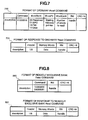
- Fig. 7 shows an example of format of an ordinary readout command to be transmitted to the RFID tag 100 (i.e., a readout command to the banks other than the readout exclusive bank), and an example of format of a response to the ordinary readout command, to be transmitted from the RFID tag 100 back to the RFID reader/writer apparatus 101 or 102.
- the ordinary readout command is built up with, as is shown by a command format 700, a field for storing a command code value of so-called "Command”, a field for storing a parameter designating a bank as a readout target, so-called “MemBank”, and a field for storing a parameter designating a kind of a pointer, so-called "WordPtr”, therein, etc.
- the response to the ordinary readout command is built up with, as is shown by a response format 701, a field for storing a header, and a field for storing the data readout, so-called "Memory Word", therein, etc.
- Fig. 8 shows an example of format of a readout command to the readout exclusive bank, to be transmitted from the FRID reader/writer 101 or 102 to the RFID tag 100, and an example of format of the response to the readout command to the readout exclusive bank, to be transmitted from the RFID tag 100 back to the RFID reader/writer apparatus 101 or 102.
- the readout comment to the readout exclusive bank is built up with, as is shown by a command format 800, a field for storing a command code value of so-called "Command", and fields for storing other parameters therein, etc.
- This command format 800 has the structures completely different from the command format 700 of the ordinary readout command shown in Fig. 7, in particular, in the command code value and the parameters. Using such custom commands has no ill influence onto the existing specification.
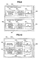
- Fig. 9 shows exemplary structures of the RFID tag 100 having the RFID tag portions corresponding to or supporting two (2) different protocols.
- the RFID tag 100 comprises a first RFID tag portion supporting a first protocol (i.e., a portion for functioning as a RFID tag in accordance with, for example, ISO 18000-6 Type C), and a second RFID tag portion supporting a second protocol (i.e., a portion for functioning as a RFID tag supporting the protocol, for example, of 2.45 GHz band) .
- the first RFID tag portion is able to re-write the data memorized therein, however within the second RFID tag portion, the data memorized therein cannot be re-written, but it can be readout only.
- the first RFID tag portion comprises an antenna 900 for transmitting radio waves between an external RFID reader/writer apparatus, a first RFID tag main body 901, a RF portion 902 for producing operating electric power from the radio waves received on the antenna 900, as well as, formodulating/demodulating signals carried on those radio waves, a RFID tag protocol process portion 903 for conducting transmission of commands and data presented by those signals, reading/writing of data from/into a plural number of memory banks within a re-writable memory portion 904, which will be mentioned below, processing of a protocol including management of the internal condition of the first RFID tag main body 901, and the re-writable memory portion 904 for memorizing various kinds of data therein, such as, ID data and user data, etc.
- the RESERVED bank the UII bank
- the TID bank the USER bank mentioned above.
- the second RFID tag portion comprises an antenna 905 for transmitting radio waves between an external RFID reader/writer apparatus, a second RFID tag main body 906, a RF portion 907 for producing operating electric power from the radio waves received on the antenna 900, as well as, for modulating/demodulating signals carried on those radio waves, a RFID tag protocol process portion 908 for conducting transmission of commands and data presented by those signals, reading/writing of data from/into a plural number of memory banks within a re-writable memory portion 909, which will be mentioned below, processing of a protocol including management of the internal condition of the second RFID tag main body 906, and a readout exclusive memory portion storing the RFID group identifier information and/or the individual information, etc., therein.
- the readout exclusive memory portion 909 is used as the readout exclusive bank mentioned above. For accessing to the readout exclusive memory portion 909, it is necessary to be conducted with a protocol different from that for other memory banks, i.e., a second protocol, different from the first protocol in accordance with the regulation or standard for the existing RFID tag.
- a protocol different from that for other memory banks i.e., a second protocol, different from the first protocol in accordance with the regulation or standard for the existing RFID tag.
- the RFID tag 100 may have three (3) or more of RFID tags, or alternately it may comprises a plural number of RFID tag portions supporting the protocols which are completely same to each other.
- Fig. 10 shows an example of the internal structures of the RFID reader/writer apparatus communicable with the RFID tags, which support the two (2) different protocols, as shown in Fig. 9.
- the RFID reader/writer apparatus 102 comprises an antenna 1000 for transmitting the radio waves between the RFID tag 100, a reader/writer apparatus main body 1001, a RF portion 1002 for modulating/demodulating of signals, which present command and data of the first protocol, a RFID protocol process portion 1003 for conducting transmission of commands and data of the first protocol, as well as, processing of a protocol, including management of an internal condition of' the RFID reader/writer apparatus 102 operating on the first protocol, etc., a RF portion 1004 for modulating/demodulating signals presenting the command and data of the second protocol, a conducting a calculation process of cryptograph and/or a signature with using a common key and/or a public key, and also execution of a hash function, etc., and an external I/F portion 305 functioning as a management device communication interface for obtaining an operation in cooperation with an external management device or apparatus (not shown in the figure).
- the different RF portions and the different protocol process portions are provided as for the different protocols, for the purpose of easy under standing thereof, however as a variation thereof, processing may be made on the different protocols within one (1) piece of the RF portion and one (1) piece of the protocol process portion.
- Fig. 11 is a view for showing the processing flow for a user to verify the properness of the UII data within the RFID tag 100.
- the RFID tag 100 is one of the RFID tags, i.e., "FRID 1", belonging to the RFID group "01", as is shown in Fig. 6, exemplarily.
- the RFID tag may be any one of the RFID tags belonging to the RFID groups "01" to "03".
- the process shown in Fig. 11 can be executed for a user of the FRID tag 100, at any time depending upon necessity thereof.
- the RFID group identification information "01" and the individual information "000001” are stored into the readout exclusive bank of the RFID tag 100, and into the UII bank is stored the UII data "00000001", respectively.
- the activity of storing the RFID group identification information "01” and the individual information "000001" into the readout exclusive bank is made by a maker of the RFID tag 100, for example, before shipping of that RFID tag 100.
- the activity of storing the UII data "00000001" is conducted by the user, for example.
- the process flow in a first half shown in Fig. 11 shows the processing, for such the user as mentioned above, to store the cryptography process result data for verifying the properness of the UII data into the RFID tag 100. Therefore, at a time instance of starting the process flow shown in Fig. 11, that cryptography process result data mentioned above is not yet stored into the RFID tag 100.
- a process is executed for reading out the UII data within the RFID tag 100, between the RFID reader/writer apparatus 101, which the above-mentioned user uses, and the RFID tag 100.
- a command for reading out the UII bank is transmitted from the RFID reader/writer apparatus 101 to the RFID tag 100.
- a response i.e., the UII data "00000001".
- a step S1101 is executed a process for reading out the RFID identification information within the readout exclusive bank in the RFID tag 100, between the RFID reader/writer apparatus 101 and the RFID tag 100.
- the readout command to the readout exclusive bank is transmitted from the RFID reader/writer apparatus 101 to the RFID tag 100.
- the RFID group identification information "01" and the individual information "000001", which are read out from the readout exclusive bank are responded from the RFID tag 100 to the RFID reader/writer apparatus 101.
- the calculation process of cryptograph is executed within the.RFID reader/writer apparatus 101.
- the data combining the RFID group identification information "01" and the individual information "000001", and the UII data "00000001” is delivered to the cryptography process function 400, as a calculation target data 401, and the cryptography process function 400 delives the data "4624652" for verifying the properness of the UII data, as the cryptography process result data 403.
- the examples of the key data 402, as well as, the cryptography process function 400, are not shown, in more details thereof, however those are managed by the user who uses RFID group identification information "01".
- a writing process is executed for the cryptography process result data "4624652" mentioned above.
- the RFID reader/writer apparatus 101 transmits the write-in command for writing the above-mentioned cryptography process result data "4624652" into the USER bank, to the RFID tag 100.
- the RFID tag 100 Upon receipt of that write-in command, the RFID tag 100 stored the data "4624652" for use of UII verification, using the RFID identification information in the readout exclusive bank, practically, into the USER bank.
- this RFID tag 100 After storing the data "4624652" for use of UII verification, in the manner as was mentioned above, if this RFID tag 100 is used in a distribution business or industry, then this RFID tag 100 will be distributed from one to another, among various users.
- the user who has an authority of using the key data 402 and the cryptography process function 400 is able to verify on whether the UII data within the RFID tag 100 is a proper one or not (in other words, whether the RFID tag 100 is a copy (i.e., a duplicate) or not of the other RFID tag), with using the RFID reader/writer apparatus 102, through the process flow shown in the second half in Fig. 11.
- a process is executed of reading out the UII data, between the RFID reader/writer apparatus 102 and the RFID tag 100.
- a readout command is transmitted from the RFID reader/writer apparatus 102 to the RFID tag 100, and then the UII data "00000001" is responded from the RFID tag 100 back to the RFID reader/writer apparatus 102.
- a readout command to the readout exclusive bank is transmitted from the RFID reader/writer apparatus 102 to the RFID tag 100, and then the RFID group identification information "01" and the individual information "000001" are responded from the RFID tag 100 back to the RFID reader/writer apparatus 102.
- a step S1106 is executed the calculation process of cryptograph.
- the RFID group identification information "01”, the individual information "000001", and the UII data "00000001” are delivered to the cryptography process function 400, as the calculation target data 401, and the cryptography process function 400 derives the data "4624652" for verifying the properness of the UII data, as the cryptography process result data 403.
- a process is executed for reading out the cryptography process result data stored in the USER bank.
- a USER bank readout command is transmitted from the RFID reader/writer apparatus 102 to the RFID tag 100, and then the cryptography process result data "4624652" is responded from the RFID tag 100 to the RFID reader/writer apparatus 102.
- a process is executed for verifying the properness of the calculation target data.
- the RFID protocol process portion compares the cryptography process result data calculated in the step S1106 and the cryptography process result data read out in the step S1107, and if they are coincident with, it is determined that the UII data within the RFID tag 100 is proper data.
- the RFID reader/writer apparatus 102 informs an error to the user.
- the third party since the third party, not knowing the key data 402, is unable to obtain the proper or correct cryptography process result data, then it is impossible for the third party to verify the properness of the UII data within the RFID tag 100. This verification may be made, when it is necessary only by a proper user, for example.
- the ordinary readout of the UII data can be made, but without any problem, with the protocol according to the existing specification.
Landscapes
- Engineering & Computer Science (AREA)
- Computer Security & Cryptography (AREA)
- Computer Hardware Design (AREA)
- Theoretical Computer Science (AREA)
- Software Systems (AREA)
- Physics & Mathematics (AREA)
- General Engineering & Computer Science (AREA)
- General Physics & Mathematics (AREA)
- Storage Device Security (AREA)
- Credit Cards Or The Like (AREA)
Applications Claiming Priority (1)
| Application Number | Priority Date | Filing Date | Title |
|---|---|---|---|
| JP2006231616A JP4974613B2 (ja) | 2006-08-29 | 2006-08-29 | Icメモリ並びにicメモリ用のアクセス装置及び正当性検証方法 |
Publications (2)
| Publication Number | Publication Date |
|---|---|
| EP1916546A2 true EP1916546A2 (de) | 2008-04-30 |
| EP1916546A3 EP1916546A3 (de) | 2011-09-07 |
Family
ID=39182083
Family Applications (1)
| Application Number | Title | Priority Date | Filing Date |
|---|---|---|---|
| EP07252994A Withdrawn EP1916546A3 (de) | 2006-08-29 | 2007-07-30 | Speicher mit integrierter Schaltung sowie Zugriffsvorrichtung und Gültigkeitsprüfverfahren für die Verwendung des Speichers mit integrierter Schaltung |
Country Status (3)
| Country | Link |
|---|---|
| US (1) | US20080094183A1 (de) |
| EP (1) | EP1916546A3 (de) |
| JP (1) | JP4974613B2 (de) |
Cited By (1)
| Publication number | Priority date | Publication date | Assignee | Title |
|---|---|---|---|---|
| WO2009148273A3 (ko) * | 2008-06-04 | 2010-11-04 | 한국전자통신연구원 | Rfid 서비스를 위한 rfid 태그 및 그의 rfid 서비스 방법 |
Families Citing this family (11)
| Publication number | Priority date | Publication date | Assignee | Title |
|---|---|---|---|---|
| US8698604B2 (en) * | 2005-04-25 | 2014-04-15 | Lg Electronics Inc. | Reader control system |
| CN101246538A (zh) * | 2007-02-14 | 2008-08-20 | 日电(中国)有限公司 | 射频识别系统和方法 |
| JP4521678B2 (ja) * | 2007-11-19 | 2010-08-11 | フェリカネットワークス株式会社 | 通信システム、情報処理方法、プログラム、及び情報処理装置 |
| US7795895B2 (en) * | 2007-11-28 | 2010-09-14 | Mstar Semiconductor, Inc. | Loop-back testing method and apparatus for IC |
| US8712334B2 (en) | 2008-05-20 | 2014-04-29 | Micron Technology, Inc. | RFID device using single antenna for multiple resonant frequency ranges |
| US8320570B2 (en) * | 2008-12-05 | 2012-11-27 | Electronics And Telecommunications Research Institute | Apparatus and method for generating secret key |
| WO2011064833A1 (ja) * | 2009-11-24 | 2011-06-03 | 三菱電機株式会社 | 情報処理装置及び情報処理方法及びプログラム |
| KR101139726B1 (ko) | 2010-10-04 | 2012-04-26 | 인크로스 주식회사 | Rfid 태그에서 유저 메모리 영역 사용을 통한 uii 영역 확장 방법 |
| JP5991160B2 (ja) * | 2012-11-19 | 2016-09-14 | ソニー株式会社 | ディスクカートリッジおよびチェンジャー |
| US10149135B1 (en) * | 2017-05-30 | 2018-12-04 | Illinois Tool Works Inc. | Methods and apparatuses for wireless communication with a brush |
| JP7802714B2 (ja) * | 2023-01-20 | 2026-01-20 | 東芝テック株式会社 | 媒体処理装置 |
Family Cites Families (11)
| Publication number | Priority date | Publication date | Assignee | Title |
|---|---|---|---|---|
| US5036461A (en) * | 1990-05-16 | 1991-07-30 | Elliott John C | Two-way authentication system between user's smart card and issuer-specific plug-in application modules in multi-issued transaction device |
| DE4205567A1 (de) * | 1992-02-22 | 1993-08-26 | Philips Patentverwaltung | Verfahren zum steuern des zugriffs auf einen speicher sowie anordnung zur durchfuehrung des verfahrens |
| JPH09282433A (ja) * | 1996-04-12 | 1997-10-31 | Nhk Spring Co Ltd | セキュリティシステム |
| US7239226B2 (en) * | 2001-07-10 | 2007-07-03 | American Express Travel Related Services Company, Inc. | System and method for payment using radio frequency identification in contact and contactless transactions |
| US6957333B2 (en) * | 2002-09-12 | 2005-10-18 | Symbol Technologies, Inc. | System and method for encrypted communications between electronic devices |
| US20050049979A1 (en) * | 2003-08-26 | 2005-03-03 | Collins Timothy J. | Method, apparatus, and system for determining a fraudulent item |
| JP4664035B2 (ja) * | 2004-10-18 | 2011-04-06 | シャープ株式会社 | 機能性icタグ |
| WO2006059554A1 (en) * | 2004-12-03 | 2006-06-08 | Semiconductor Energy Laboratory Co., Ltd. | Semiconductor device |
| JP4954537B2 (ja) * | 2004-12-03 | 2012-06-20 | 株式会社半導体エネルギー研究所 | 半導体装置 |
| US8698604B2 (en) * | 2005-04-25 | 2014-04-15 | Lg Electronics Inc. | Reader control system |
| US20070194879A1 (en) * | 2005-05-02 | 2007-08-23 | International Business Machines Corporation | Method and device for detecting an invalid RFID tag and method for manufacturing an RFID tag |
-
2006
- 2006-08-29 JP JP2006231616A patent/JP4974613B2/ja not_active Expired - Fee Related
-
2007
- 2007-07-30 EP EP07252994A patent/EP1916546A3/de not_active Withdrawn
- 2007-07-31 US US11/830,982 patent/US20080094183A1/en not_active Abandoned
Cited By (2)
| Publication number | Priority date | Publication date | Assignee | Title |
|---|---|---|---|---|
| WO2009148273A3 (ko) * | 2008-06-04 | 2010-11-04 | 한국전자통신연구원 | Rfid 서비스를 위한 rfid 태그 및 그의 rfid 서비스 방법 |
| US9208360B2 (en) | 2008-06-04 | 2015-12-08 | Electronics And Telecommunications Research Institute | RFID tag for RFID service and RFID service method thereof |
Also Published As
| Publication number | Publication date |
|---|---|
| JP2008059013A (ja) | 2008-03-13 |
| US20080094183A1 (en) | 2008-04-24 |
| JP4974613B2 (ja) | 2012-07-11 |
| EP1916546A3 (de) | 2011-09-07 |
Similar Documents
| Publication | Publication Date | Title |
|---|---|---|
| EP1916546A2 (de) | Speicher mit integrierter Schaltung sowie Zugriffsvorrichtung und Gültigkeitsprüfverfahren für die Verwendung des Speichers mit integrierter Schaltung | |
| CN108053001B (zh) | 电子仓单的信息安全认证方法和系统 | |
| US7872567B2 (en) | Method for transponder access control | |
| US7999659B2 (en) | Method for access control | |
| US7873767B2 (en) | Wireless IC memory, accessing apparatus for use of wireless IC memory, accessing control method for use of wireless IC memory, and wireless IC memory system | |
| US20090033464A1 (en) | Transponder with access protection and method for access to the transponder | |
| US5379344A (en) | Smart card validation device and method | |
| AU2006203517B2 (en) | Using Promiscuous and Non-Promiscuous Data to Verify Card and Reader Identity | |
| US20080012685A1 (en) | Scalable method for access control | |
| US20070176744A1 (en) | Mobile communication terminal having a function of reading out information from contactless type communication tag and method for providing information of whether an article is genuine or not | |
| EP2474936A1 (de) | Digitales identifizierungsgerät für produktkennung, prüfgerät, produkt und verfahren für produktüberprüfung und fälschungsschutz | |
| US20090315673A1 (en) | RFID Tag And Operating Method Thereof | |
| KR100512064B1 (ko) | 제품의 진품 여부를 확인하기 위한 비접촉식 통신 태그 및 휴대형 태그 판독기 | |
| JP5107934B2 (ja) | 通信制御方法、rfid装置及びrfidシステム | |
| US20050134436A1 (en) | Multiple RFID anti-collision interrogation method | |
| AU2006238975B2 (en) | Method of migrating RFID transponders in situ | |
| KR100524176B1 (ko) | 알에프 태그에 저장된 제품 확인 정보를 판독할 수 있는이동통신 단말기 및 그 단말기와 통신하는 컴퓨터에서실행 가능한 서비스 관리 방법 | |
| KR100848791B1 (ko) | 보안 검증이 가능한 태그 데이터 기록 및 취득 방법, 태그데이터 기록 및 취득 장치 | |
| JP2008233975A (ja) | 情報通信装置、情報集中管理装置、及び情報処理システム | |
| CN115066684B (zh) | 用于验证射频识别号码的方法 | |
| CN102708393B (zh) | 监控应答器中应用数据的访问的应答器、方法及读取器 | |
| CN101625727B (zh) | 射频识别标签及其运作方法 | |
| JP2008305303A (ja) | Rfidタグ管理システムおよびrfidタグ | |
| EP3771145A1 (de) | Verfahren zur validierung und zuteilung von codes, und entsprechendes system | |
| JP2008152392A (ja) | 無線タグ、無線タグリーダ、復号装置、無線タグの制御方法、及び無線タグの管理方法 |
Legal Events
| Date | Code | Title | Description |
|---|---|---|---|
| PUAI | Public reference made under article 153(3) epc to a published international application that has entered the european phase |
Free format text: ORIGINAL CODE: 0009012 |
|
| 17P | Request for examination filed |
Effective date: 20070820 |
|
| AK | Designated contracting states |
Kind code of ref document: A2 Designated state(s): AT BE BG CH CY CZ DE DK EE ES FI FR GB GR HU IE IS IT LI LT LU LV MC MT NL PL PT RO SE SI SK TR |
|
| AX | Request for extension of the european patent |
Extension state: AL BA HR MK RS |
|
| PUAL | Search report despatched |
Free format text: ORIGINAL CODE: 0009013 |
|
| AK | Designated contracting states |
Kind code of ref document: A3 Designated state(s): AT BE BG CH CY CZ DE DK EE ES FI FR GB GR HU IE IS IT LI LT LU LV MC MT NL PL PT RO SE SI SK TR |
|
| AX | Request for extension of the european patent |
Extension state: AL BA HR MK RS |
|
| RIC1 | Information provided on ipc code assigned before grant |
Ipc: G06F 21/00 20060101ALI20110804BHEP Ipc: G01V 15/00 20060101AFI20110804BHEP |
|
| AKX | Designation fees paid |
Designated state(s): DE FR GB |
|
| STAA | Information on the status of an ep patent application or granted ep patent |
Free format text: STATUS: THE APPLICATION IS DEEMED TO BE WITHDRAWN |
|
| 18D | Application deemed to be withdrawn |
Effective date: 20150203 |