EP1916708A2 - Dessin de porte en silicium polycristallin dopé - Google Patents
Dessin de porte en silicium polycristallin dopé Download PDFInfo
- Publication number
- EP1916708A2 EP1916708A2 EP07119098A EP07119098A EP1916708A2 EP 1916708 A2 EP1916708 A2 EP 1916708A2 EP 07119098 A EP07119098 A EP 07119098A EP 07119098 A EP07119098 A EP 07119098A EP 1916708 A2 EP1916708 A2 EP 1916708A2
- Authority
- EP
- European Patent Office
- Prior art keywords
- layer
- rare earth
- silicon
- plasma
- gate
- Prior art date
- Legal status (The legal status is an assumption and is not a legal conclusion. Google has not performed a legal analysis and makes no representation as to the accuracy of the status listed.)
- Granted
Links
Images


Classifications
-
- H—ELECTRICITY
- H10—SEMICONDUCTOR DEVICES; ELECTRIC SOLID-STATE DEVICES NOT OTHERWISE PROVIDED FOR
- H10P—GENERIC PROCESSES OR APPARATUS FOR THE MANUFACTURE OR TREATMENT OF DEVICES COVERED BY CLASS H10
- H10P50/00—Etching of wafers, substrates or parts of devices
- H10P50/60—Wet etching
- H10P50/66—Wet etching of conductive or resistive materials
- H10P50/663—Wet etching of conductive or resistive materials by chemical means only
- H10P50/667—Wet etching of conductive or resistive materials by chemical means only by liquid etching only
-
- H—ELECTRICITY
- H10—SEMICONDUCTOR DEVICES; ELECTRIC SOLID-STATE DEVICES NOT OTHERWISE PROVIDED FOR
- H10D—INORGANIC ELECTRIC SEMICONDUCTOR DEVICES
- H10D64/00—Electrodes of devices having potential barriers
- H10D64/01—Manufacture or treatment
- H10D64/013—Manufacture or treatment of electrodes having a conductor capacitively coupled to a semiconductor by an insulator
- H10D64/01302—Manufacture or treatment of electrodes having a conductor capacitively coupled to a semiconductor by an insulator the insulator being formed after the semiconductor body, the semiconductor being silicon
- H10D64/01304—Manufacture or treatment of electrodes having a conductor capacitively coupled to a semiconductor by an insulator the insulator being formed after the semiconductor body, the semiconductor being silicon characterised by the conductor
- H10D64/01306—Manufacture or treatment of electrodes having a conductor capacitively coupled to a semiconductor by an insulator the insulator being formed after the semiconductor body, the semiconductor being silicon characterised by the conductor the conductor comprising a layer of silicon contacting the insulator, e.g. polysilicon
-
- H—ELECTRICITY
- H10—SEMICONDUCTOR DEVICES; ELECTRIC SOLID-STATE DEVICES NOT OTHERWISE PROVIDED FOR
- H10D—INORGANIC ELECTRIC SEMICONDUCTOR DEVICES
- H10D64/00—Electrodes of devices having potential barriers
- H10D64/01—Manufacture or treatment
- H10D64/013—Manufacture or treatment of electrodes having a conductor capacitively coupled to a semiconductor by an insulator
- H10D64/01302—Manufacture or treatment of electrodes having a conductor capacitively coupled to a semiconductor by an insulator the insulator being formed after the semiconductor body, the semiconductor being silicon
- H10D64/01304—Manufacture or treatment of electrodes having a conductor capacitively coupled to a semiconductor by an insulator the insulator being formed after the semiconductor body, the semiconductor being silicon characterised by the conductor
- H10D64/01318—Manufacture or treatment of electrodes having a conductor capacitively coupled to a semiconductor by an insulator the insulator being formed after the semiconductor body, the semiconductor being silicon characterised by the conductor the conductor comprising a layer of alloy material, compound material or organic material contacting the insulator, e.g. TiN
-
- H—ELECTRICITY
- H10—SEMICONDUCTOR DEVICES; ELECTRIC SOLID-STATE DEVICES NOT OTHERWISE PROVIDED FOR
- H10P—GENERIC PROCESSES OR APPARATUS FOR THE MANUFACTURE OR TREATMENT OF DEVICES COVERED BY CLASS H10
- H10P50/00—Etching of wafers, substrates or parts of devices
- H10P50/20—Dry etching; Plasma etching; Reactive-ion etching
- H10P50/26—Dry etching; Plasma etching; Reactive-ion etching of conductive or resistive materials
- H10P50/264—Dry etching; Plasma etching; Reactive-ion etching of conductive or resistive materials by chemical means
- H10P50/266—Dry etching; Plasma etching; Reactive-ion etching of conductive or resistive materials by chemical means by vapour etching only
- H10P50/267—Dry etching; Plasma etching; Reactive-ion etching of conductive or resistive materials by chemical means by vapour etching only using plasmas
-
- H—ELECTRICITY
- H10—SEMICONDUCTOR DEVICES; ELECTRIC SOLID-STATE DEVICES NOT OTHERWISE PROVIDED FOR
- H10P—GENERIC PROCESSES OR APPARATUS FOR THE MANUFACTURE OR TREATMENT OF DEVICES COVERED BY CLASS H10
- H10P50/00—Etching of wafers, substrates or parts of devices
- H10P50/20—Dry etching; Plasma etching; Reactive-ion etching
- H10P50/26—Dry etching; Plasma etching; Reactive-ion etching of conductive or resistive materials
- H10P50/264—Dry etching; Plasma etching; Reactive-ion etching of conductive or resistive materials by chemical means
- H10P50/266—Dry etching; Plasma etching; Reactive-ion etching of conductive or resistive materials by chemical means by vapour etching only
- H10P50/267—Dry etching; Plasma etching; Reactive-ion etching of conductive or resistive materials by chemical means by vapour etching only using plasmas
- H10P50/268—Dry etching; Plasma etching; Reactive-ion etching of conductive or resistive materials by chemical means by vapour etching only using plasmas of silicon-containing layers
-
- H—ELECTRICITY
- H10—SEMICONDUCTOR DEVICES; ELECTRIC SOLID-STATE DEVICES NOT OTHERWISE PROVIDED FOR
- H10P—GENERIC PROCESSES OR APPARATUS FOR THE MANUFACTURE OR TREATMENT OF DEVICES COVERED BY CLASS H10
- H10P30/00—Ion implantation into wafers, substrates or parts of devices
- H10P30/20—Ion implantation into wafers, substrates or parts of devices into semiconductor materials, e.g. for doping
- H10P30/202—Ion implantation into wafers, substrates or parts of devices into semiconductor materials, e.g. for doping characterised by the semiconductor materials
- H10P30/204—Ion implantation into wafers, substrates or parts of devices into semiconductor materials, e.g. for doping characterised by the semiconductor materials into Group IV semiconductors
-
- H—ELECTRICITY
- H10—SEMICONDUCTOR DEVICES; ELECTRIC SOLID-STATE DEVICES NOT OTHERWISE PROVIDED FOR
- H10P—GENERIC PROCESSES OR APPARATUS FOR THE MANUFACTURE OR TREATMENT OF DEVICES COVERED BY CLASS H10
- H10P30/00—Ion implantation into wafers, substrates or parts of devices
- H10P30/20—Ion implantation into wafers, substrates or parts of devices into semiconductor materials, e.g. for doping
- H10P30/208—Ion implantation into wafers, substrates or parts of devices into semiconductor materials, e.g. for doping of electrically inactive species
-
- H—ELECTRICITY
- H10—SEMICONDUCTOR DEVICES; ELECTRIC SOLID-STATE DEVICES NOT OTHERWISE PROVIDED FOR
- H10P—GENERIC PROCESSES OR APPARATUS FOR THE MANUFACTURE OR TREATMENT OF DEVICES COVERED BY CLASS H10
- H10P32/00—Diffusion of dopants within, into or out of wafers, substrates or parts of devices
- H10P32/30—Diffusion for doping of conductive or resistive layers
- H10P32/302—Doping polycrystalline silicon or amorphous silicon layers
Definitions
- the present invention is related to the field of semiconductor processing. More specifically it is related to the patterning of poly-Silicon (Poly-Si) doped with an element that does not form volatile compounds during conventional reactive ion etching.
- Poly-Si poly-Silicon
- the invention is further related to a method to pattern Ytterbium (Yb) doped poly-Si (gates) or in other words makes it possible to etch Yb doped poly-Si gates using a combination of dry and wet etching.
- Yb Ytterbium
- the transistor's work function can be modulated using dopants in combination with fully silicided gates.
- the use of an activation anneal of these dopants has been shown to have a strong effect on the work function modulation achieved.
- Aluminium (Al) can be used as dopant to fabricate poly-Si gate for p-MOS transistors whereas Ytterbium (Yb) doped poly-Si gate will be used for n-MOS transistors.
- CMOS complementary MOS
- the gates might receive the implants (Yb and Al) before the gate patterning or just before the silicidation. In the former case they can receive the anneal from the junction anneal, whereas in the latter case they will not get an activation anneal because the integrity of the NiSi source drain regions could not be preserved.
- the present invention provides a method for etching poly-Si gates doped with an element, in particular a rare earth, that does not form volatile compounds during conventional reactive ion etching, such as Ytterbium (Yb).
- an element in particular a rare earth, that does not form volatile compounds during conventional reactive ion etching, such as Ytterbium (Yb).
- the invention further provides a method for patterning a gate structure comprising Lanthanide elements, preferably Ytterbium, using a combination of a dry etch plasma and a wet removal step, thereby avoiding micromasking and unwanted residues.
- the present invention provides a method for the manufacture of a semiconductor device comprising selectively removing, at least partly, a rare earth doped layer over a layer underneath, said selective removal comprising the steps of:
- the resulting chlorinated and/or brominated layer dissolve(s) in the aqueous solution (preferably in water).
- the resulting chlorinated and/or brominated rare earth(s) being water soluble, are removed with an aqueous solution, preferably with water.
- said subjecting step and said contacting step can be repeated (at least once). More particularly, said subjecting step and said contacting step can be repeated for the complete removal of said rare earth doped layer, said removal being possibly limited to a delimited (or restricted) area.
- said plasma is preferably anisotropically applied, whereby a delimited area is chlorinated and/or brominated.
- said rare earth(s) is/are selected from the group consisting of Sc, Y, La, Dy, Pr, Nd, Gd, Tb, Ho, Er, Tm, Yb and Lu. More preferably, said rare earth(s) is/are selected from the lanthanides.
- said rare earth is ytterbium, Yb.
- said rare earth(s) in said doped layer is/are in a concentration of less than 10%, more preferably of less than 5%, more preferably of less than 2%, and even more preferably of less than 1%, but not null (i.e. higher than 0).
- said Cl-comprising plasma is preferably a Cl 2 and/or BCl 3 comprising plasma.
- said Br-comprising plasma is preferably a HBr and/or Br 2 comprising plasma.
- said chlorination and said bromination can be performed sequentially, both orders being envisaged, or can be performed simultaneously.
- Cl-comprising plasma and/or Br-comprising plasma also encompasses a Cl- and/or Br-comprising plasma.
- said Cl- and/or Br-comprising plasma does not contain fluorine or fluorine containing compounds.
- inert compounds such as argon, helium, and/or nitrogen can be added to said plasma.
- said rare earth doped layer consists of a layer suitable for dry-etching, wherein said rare earth(s) has/have been introduced.
- the matrix or main composition of said layer is suitable for dry-etching, while said introduced rare earth(s) need to be chlorinated and/or brominated for further removal with an aqueous solution, preferably with water (by contacting or rinsing).
- Said doped layer can consist of a metal layer suitable for dry-etching, wherein said rare earth(s) has/have been introduced.
- Said doped layer can consist of a silicon, silicon-oxide, silicon-germanide, silicon-nitride, silicon-carbide, silicon-oxy-carbide, or germanium layer, wherein said rare earth(s) has/have been introduced.
- said layer underneath is polycrystalline silicon.
- said layer underneath is a substrate.
- Said substrate can comprise (or consist of) silicon (preferably polycrystalline silicon), silicon-oxide, silicon-germanide, silicon-nitride, silicon-carbide, silicon-oxy-carbide, or germanium.
- said substrate is polycrystalline silicon.
- a method for the manufacture of a semiconductor device comprising selectively removing, at least partly, a rare earth doped layer over a layer underneath according to the present invention can be used for patterning a structure, such as a gate structure in a semiconductor device.
- a method for patterning a stack of layers comprising at least one rare earth doped layer comprising the steps of:
- a method for patterning can further comprise, before the step of developing a mask structure, the steps of:
- the step of annealing is performed at a temperature comprised between about 700°C and about 1100°C.
- the step of annealing is performed using a thermal anneal at 950°C (e.g. in a furnace or in a Rapid Thermal Annealing Tool).
- the step of annealing can also be performed using a laser anneal.
- said structure is a gate structure in a semiconductor device, said rare earth doped layer is a gate electrode layer.
- a gate dielectric layer is deposited before the step of depositing the gate electrode layer.
- said doped layer, used as a gate electrode layer is a poly-crystalline silicon layer and said underneath layer, used as a gate dielectric, is a high-k layer (i.e. a layer of a material having a dielectric constant, k, higher than that of SiO 2 ), a SiO 2 layer, or a SiON layer.
- Said gate dielectric layer can be further etched to complete the gate structure.
- Figure 1A illustrates a tilted SEM picture of an Yb-doped poly-Si gate after etch using conventional poly-Si gate etch recipe.
- Figure 1B illustrates a tilted SEM picture of an Yb-doped poly-Si gate after etch using a conventional poly-Si gate etch recipe and an anneal in N 2 at 900°C to distribute the Yb in the poly-Si layer.
- Figure 2 illustrates a flowchart according to a preferred embodiment of the invention to perform the dry/wet/dry etch approach for patterning of poly-Si doped with almost non-volatile elements (e.g. Yb).
- Yb non-volatile elements
- Figure 3A up to Figure 31 illustrate the different processing steps according to a preferred embodiment of the invention to perform the dry/wet/dry etch approach for patterning of poly-Si doped with almost non-volatile elements (e.g. Yb).
- Yb non-volatile elements
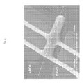
- Figure 4 shows a tilted SEM of a ring oscillator structure where the poly-Si is Yb-doped for n-MOS and Aldoped for p-MOS after full dry-wet-dry etch process according to the present invention.
- the present invention relates to a method for the patterning of a stack comprising elements that do not form volatile compounds during conventional reactive ion etching.
- Lanthanide elements such as Ytterbium (Yb) and the patterning preferably relates to the dry etching of silicon and/or germanium comprising structures (e.g. gates) doped with a Lanthanide e.g. Ytterbium (Yb doped gates).
- said silicon and/or germanium comprising structure is a gate electrode
- the silicon and/or germanium is doped with a Lanthanide (e.g. Yb) for tuning the work function of a gate electrode.
- a Lanthanide e.g. Yb
- a method for the patterning of a Si, Ge or SiGe comprising gate electrode layer further comprising one or more lanthanide dopants in a semiconductor device.
- Said method comprises the steps of first providing a substrate comprising a gate dielectric layer and depositing a gate electrode layer onto said gate dielectric layer.
- the gate electrode layer is doped with a suitable doping element (dopant).
- Said dopant is characterized as a Lanthanide element which does not form volatile compounds during conventional reactive ion etching such as Ytterbium (Yb).
- a mask structure is developed onto said gate electrode layer to define a gate structure and to expose part(s) of the gate electrode layer.
- the exposed parts of the gate electrode layer are chlorinated (and/or brominated) using an halogen comprising plasma such that the dopant is chlorinated (and/or brominated).
- Said halogen comprising plasma is a Cl comprising plasma (and/or Br comprising plasma) that does not contain F.
- chlorinated (and/or brominated) doping elements also referred to as dopants
- dopants also referred to as dopants
- said wet etch step is a water rinse or alternatively a rinse using an acidified water based solution.
- An example of said acidified solution can be HCl in water wherein the HCl concentration can range from 1-2% till 10-20%.
- the substrate is then transferred to the dry etch chamber to perform a dry etch step to etch the remaining part of the gate electrode layer and optionally gate dielectric layer.
- an anneal step is performed, said anneal step is preferably a thermal anneal.
- the anneal step is performed after the step of (selectively) removing the halogenated dopants after the step of patterning the complete gate electrode.
- the step of subjecting the exposed parts of the gate electrode layer to an halogen comprising plasma is performed in a dry etch chamber using an anisotropic dry-etch plasma.
- Said dry etch chamber can be the same etch chamber in which the patterning of the gate structure is completed.
- the step of subjecting the exposed parts of the gate electrode layer is performed by an anisotropic dry-etch plasma during the step of patterning said gate electrode layer using a Cl (and/or Br) based (or comprising) plasma whereby during the etching the exposed portions of said gate dielectric layer gets chlorinated (and/or brominated).
- the Cl (and/or Br) based (or comprising) plasma is a Cl 2 , HBr or BCl 3 comprising plasma.
- said Cl comprising plasma and/or Br comprising plasma can comprise a combination of two or three of Cl 2 , HBr and BCl 3 .
- the substrate is a silicon wafer.
- an interlayer is deposited onto said substrate before depositing the gate dielectric layer.
- the substrate bias during the step of subjecting the exposed parts of the gate electrode layer to a Cl- (and/or Br-) based (or comprising) plasma is 75W to 300W.
- the plasma power during the step of subjecting the exposed parts of the gate electrode layer to a Cl- (and/or Br-) based (or comprising) plasma is in the range of 100W up to 1200W.
- the plasma power during the step of subjecting the exposed parts of the gate electrode layer to a Cl- (and/or Br-) based (or comprising) plasma is around 250W.
- the pressure in the plasma during the step of subjecting the exposed parts of the gate electrode layer to a Cl (and/or Br) based (or comprising) plasma is minimum 0.666Pa (5mT) and maximum 10.665Pa (80mT).
- the pressure in the plasma during the step of subjecting the exposed parts of the gate electrode layer to a Cl- (and/or Br-) based (or comprising) plasma is 0.799Pa (6mT).
- the method of the invention is illustrated for patterning of a gate electrode structure but is applicable to pattern any silicon and/or germanium comprising layer having a doping element as long as said doping element forms soluble halides.
- the method of the invention for patterning of a stack of layers using a combination (or sequence) of wet etch and dry etch techniques is also referred to as dry-wet-dry etch approach.
- the present invention provides a method for patterning at least one layer of a stack of layers to define a structure, said at least one layer comprising one or more Lanthanide elements and said method at least comprising the steps of:
- the Lanthanide element(s) are present in the stack of layers to be patterned in a concentration ⁇ 1%.
- said Cl-based (or Cl-comprising) (and/or Br-based or Br-comprising) plasma is a Cl 2 and/or BCl 3 and/or HBr/Br 2 comprising plasma.
- the method can further comprise, before the step of developing a mask structure, the step of:
- the step of annealing is performed using a thermal anneal at 950°C.
- said structure is a gate structure in a semiconductor device
- said deposited layer is a gate electrode layer
- the method further comprises, before the step of depositing the gate electrode layer, the step of depositing a gate dielectric layer.
- said deposited layer is a polycrystalline silicon layer to be used as a gate electrode layer and said gate dielectric layer is a high-k layer, SiO 2 layer or SiON layer.
- the method further comprises, after the step of performing a dry etch step to etch the remaining part of the gate electrode layer to define a gate electrode, the step of:
- said doping element is a Lanthanide selected from at least one of La, Ce, Pr, Nd, Pm, Sm, Eu, Gd, Tb, Dy, Ho, Er, Tm, Yb and Lu.
- said doping element is Yb.
- said substrate is a silicon wafer.
- said wet etch is a water rinse.
- the method for patterning can be used to fabricate a semiconductor device comprising a gate structure.
- substrate bias refers to the voltage applied to the substrate in a Reactive Ion Etching (RIE) chamber. This value is expressed in Watts.
- RIE Reactive Ion Etching
- a substrate bias is preferred to avoid lateral etch of the structures due to exposure to plasma components.
- anisotropic etch refers to the etching process in which etch rate in the direction perpendicular to the surface (or substrate) is much higher than in direction parallel to the surface (or substrate). This in contrast to “isotropic etch” in which the etching occurs the same in any direction or being non-directional.
- micromasking refers to and is observed when a number of the residuals behave as if they were tiny islands of etchresisting material which prevent the underlying layer from being etched and hence act as a mask. Additionally, if a continuous string of such micromasking nodules occurs undesired electrical shorts may occur. Even if complete shorts are not formed, critical electrical attributes such as current leakage may be adversely affected by micromasking.
- Lanthanides refers to the 15 elements with atomic numbers 57 through 71, from lanthanum to lutetium. More specifically and as an example it refers in this application to Lanthanides used for doping to achieve a n-type (p-type) doping of e.g. poly-silicon.
- integrated circuit includes devices formed on semiconducting substrates, such as group IV materials like silicon or germanium, or group III-V compounds like gallium arsenide, or structured substrate such as silicon-on-insulator, strained silicon and silicon-germanium, or mixtures of such materials.
- group IV materials like silicon or germanium, or group III-V compounds like gallium arsenide
- structured substrate such as silicon-on-insulator, strained silicon and silicon-germanium, or mixtures of such materials.
- the term includes all types of devices formed, such as memory and logic, and all designs of such devices, such as MOS and bipolar.
- the term also comprehends applications such as flat panel displays, solar cells, and charge coupled devices.
- the invention solves the problem of micromasking occurring during the patterning of poly-silicon gates doped with Lanthanides such as Ytterbium (Yb) using reactive ion dry-etching techniques. More specifically the problem is the removal of said dopant residues during the patterning thereby avoiding micromasking.
- the dry-etching of said Lanthanides is hardly possible at close to room temperatures due to very low volatility of Lanthanides. For example the melting point of Yb is around 824°C which is far too high to perform reactive ion etching.
- a stack of layers e.g. a gate stack layer
- elements e.g. dopants
- the invention provides a method for forming (or patterning) a structure in at least one layer (or a stack of layers) on a semiconductor substrate. More specifically said structure can be a gate structure.
- a layer is first deposited onto a substrate and doped with a suitable dopant.
- Said dopant is preferably a Lanthanide such as Yb.
- the deposited layer is then patterned with a suitable mask to define a structure in said deposited layer and to expose portions of the deposited layer.
- the exposed portions of the deposited layer are then subjected to a halogen comprising plasma that causes chlorination (and/or bromination) of the dopant in the exposed portions of the deposited layer.
- Said halogen comprising plasma is preferably an in-situ plasma comprising Cl and/or Br species (and does not comprise F species).
- the chlorinated (and/or brominated) portions of the dopants can be selectively wet etched.
- Said wet etch is preferably a water based rinse (or optionally acidified water can be used).
- the patterning of the structure is completed using dry etching techniques.
- the dopants in the patterned structure need to be distributed using an anneal. Most preferred said anneal step is a thermal anneal.
- the method of the invention is preferably used to pattern a stack of layers whereby at least one of the layers comprises a Lanthanide, preferably said stack of layers are gate stack layers.
- Said stack of layers is situated or deposited onto a substrate, most preferred said substrate is a semiconductor substrate e.g. silicon wafer.
- the aim of the patterning is to pattern or to form a gate structure in said gate stack layers.
- Said gate structure comprises at least one gate electrode (layer) and at least one gate oxide (layer) situated below said gate electrode layer.
- an interlayer can be deposited onto the substrate before depositing said gate stack layers, said interlayer can be a thermally grown SiO 2 layer.
- Said thermally grown SiO 2 can be formed by subjecting the (silicon) substrate to a HF dip (2%HF for a few minutes).
- the gate stack layer used to form the gate electrode is a silicon and/or germanium comprising layer such as a polycrystalline-silicon (poly-Si) layer.
- the gate stack layer used to form the gate oxide is a high-k layer but other suitable gate oxide layers are also possible (e.g. SiO 2 , SiON).
- the present invention solves the problem of patterning of gate electrode layers doped with one or more Lanthanide elements to tune the workfunction of a gate electrode, more specifically the selective removal of Lanthanides in a gate electrode layer during patterning of a gate structure is disclosed. Dry removal is impossible since Lanthanides do not form volatile compounds within the temperature ranges used during reactive ion etching (plasma etching).
- the present invention solves the problem of micromasking originating from Lanthanide residues during the patterning by first performing a chlorination (and/or bromination) step using a dry-etch plasma such that Lanthanide halides are formed (e.g. YbCl 3 ) which are water soluble. Said chlorination (and/or bromination) step is performed after the creation of a mask structure such that only the exposed areas are chlorinated (and/or brominated). In a second step said Lanthanide halides are selectively removed from the substrate using a wet removal step. Said wet removal step is preferably performed using a deionized water rinse or alternatively a rinse with acidified water.
- the method of the invention solves the problem by chlorinating (and/or brominating) the Lanthanides by means of a Cl and/or Br containing plasma (e.g. Cl 2 , HBr, Br 2 and/or BCl 3 ).
- a Cl and/or Br containing plasma e.g. Cl 2 , HBr, Br 2 and/or BCl 3 .
- the method of the invention further provides the advantage of selective removal of Lanthanide halides (i.e. chlorinated and/or brominated Lanthanides) only in the exposed areas and hence not under the areas protected by a (hard) mask used for patterning the gate structure.
- Lanthanide halides i.e. chlorinated and/or brominated Lanthanides
- the method of the invention furthermore provides the advantage of avoiding or eliminating the removal of non-chlorinated (and/or non-brominated) Lanthanides because these are not water soluble and hence only the chlorinated (and/or brominated) Lanthanides are removed by means of a wet rinse (preferably water).
- the plasma chlorination (and/or bromination) of the invention is anisotropic, whereby the areas of the gate electrode layer which are situated under the mask structure are not exposed and hence not chlorinated (and/or brominated) and, therefore, not removed by water.
- said chlorination or alternatively bromination step is performed after the step of doping the gate electrode layer and before the step of annealing the gate electrode layer such that the dopant elements are located in the upper (or top) region of the gate electrode layer.
- Said chlorinated (and/or brominated) dopant elements can be removed by performing a wet removal step.
- the dopant element is a Lanthanide such as Yb
- said wet removal of Yb-chlorides (and/or Yb-bromides) is preferably a water based removal, most preferred said removal is a water rinse.
- Figure 2 shows a flowchart illustrating the process flow according to a preferred embodiment of the invention wherein the dopant material is chlorinated (and/or brominated) during the patterning of the gate electrode.
- the description below is illustrated for patterning of a gate electrode structure but it must be clear that the method of the invention is applicable to pattern any silicon and/or germanium comprising layer comprising a minor concentration of one or more Lanthanide elements (e.g. ⁇ 1%) as long as said lanthanide element forms (water) soluble halides.
- Figure 3 illustrates schematically the individual steps after providing a substrate with gate dielectric layer and doped gate electrode layer and having a mask on top of the gate electrode layer to pattern the gate structure (according to the dry/wet/dry approach of the present invention).
- the method starts with providing a substrate 1, most preferred said substrate 1 is a semiconductor substrate such as a Si wafer comprising active areas (e.g. source and drain).
- a gate dielectric layer 2 is deposited e.g. a silicon dioxide layer, and/or a silicon oxynitride layer (with a thickness of e.g. 2nm) and/or a high-k layer.
- an interlayer can be deposited onto said substrate prior to the deposition of a gate dielectric layer 2, said interlayer can be e.g. a thermally grown SiO 2 layer obtained after a thermal anneal or an HF dip (e.g. a dip in a 2% HF solution).
- a gate electrode layer 3 is deposited, said gate electrode layer 3 is preferably formed with a thickness of about 100nm (range 50 nm up to maximum 200 nm), and is preferably formed of poly-crystalline silicon.
- the gate electrode layer 3 is doped with a suitable dopant element.
- a suitable dopant element is a Lanthanide and more preferred said dopant element is Ytterbium (Yb).
- Yb Ytterbium
- a poly-silicon gate layer is doped with Yb using 40keV at 4E 15 cm -2 or 8E 15 cm -2 .
- the dopant element is situated in the upper part of the gate electrode layer (or in other words near the top surface).
- a mask layer is deposited onto said gate electrode layer 5, most preferred said mask layer is a photosensitive imaging layer(s) 5, and optionally there can be a hardmask layer 4 such as silicon nitride deposited before the deposition of said photosensitive imaging layer(s) 5.
- a gate pattern is then transferred into said photosensitive imaging layer(s) 5 and hardmask layer 4 by means of photolithographic patterning.
- the (doped) gate electrode layer 6 is subjected to an halogen plasma 21, preferably said a halogen comprising plasma such that the dopant element is halogenated.
- an halogen plasma preferably said a halogen comprising plasma such that the dopant element is halogenated.
- the overlying mask structure prohibits the in-situ plasma from chlorination (and/or bromination) of the dopants in that region.
- Most preferred chlorinated and/or brominated dopants are formed in the gate electrode layer 6 which are water soluble.
- the exposed portions of the (doped) gate electrode layer 6 are subjected to a plasma comprising Cl and/or Br species that cause chlorination/bromination of the dopant elements in the gate electrode layer.
- the time and exposure of said chlorination/bromination step is such that complete chlorination/bromination of the dopants of the exposed portions of the gate electrode layer is obtained.
- the step of subjecting the exposed areas of the gate electrode layer is performed in a reactive ion etch chamber e.g. in a 2300 Versys etch chamber from Lam Research whereby the substrate bias during said exposure step is different from zero to avoid lateral exposure, a suitable substrate bias can be 90W.
- a wet removal step 22 the chlorinated and/or brominated dopants are removed from the exposed areas of the gate electrode layer 6 by means of a wet removal step 22, most preferred said wet removal step is a water rinse. Alternatively said wet removal step uses an acidified water solution. During the wet removal step, the non exposed parts of the gate electrode layer 3 (situated under the mask layer(s) 4,5 are not etched because said non-chlorinated (and/or non-brominated) dopants are not (water) soluble.
- An anisotropical dry-etching process 23 is then applied to etch (complete) a gate structure 9 in said gate electrode layer 3 and gate dielectric layer 2.
- the plasma used to pattern the gate electrode layer 3 or in other words to perform the main etch step 25 is a conventional plasma used to pattern e.g. poly crystalline silicon.
- the main etch plasma (to define 80% of the gate electrode profile) for etching of the undoped Poly-Si preferably comprises HBr, Cl 2 , CF 4 and/or O 2 as etch gases.
- a soft landing (SL) step 26 is performed whereby the etch plasma is tuned to be selective towards the underlying dielectric. This SL plays a key role for determining the bottom profile of the gate.
- the SL etch plasma preferably contains HBr and O 2 .
- an extra overetch (OE) step 27 can be applied after the SL step to clean up (Si) etch residues.
- the anisotropical dry-etching process further comprises the step of etching 28 the gate dielectric layer 2 using the above mentioned mask (gate pattern) to define a complete gate structure 9.
- the plasma can further comprise inert compounds. Finally a resist strip or removal of the mask structure 4,5 is applied.
- An anneal used to diffuse the dopants over the poly-Si layer can not be applied before the step of patterning the gate electrode layer without affecting the gate profile and needs to be applied after the step of patterning the gate electrode.
- Said thermal anneal step 29 must performed after the step of removing the halogenated dopants in the exposed areas.
- Said anneal can be performed at 950°C for 30s in N 2 ambient obtained.
- the Cl (and/or Br) comprising plasma used to perform the chlorination (and/or bromination) of the dopant element such as Yb has a plasma power in the range of 100W up to 1200W. More preferred said plasma power is around 250W.
- the pressure in the plasma chamber used to perform the chlorination (and/or bromination) of the dopant element of the present invention is in the range of minimum 0.666 Pa (5mT) and maximum 10.665 Pa (80mT). More preferred said pressure is 0.799 Pa (6mT).
- the chlorine (and/or bromine) comprising plasma used to perform the chlorination (and/or bromination) of the dopant element of the present invention has a plasma temperature below 100°C and most preferred said plasma temperature during dry-etch patterning is around 60°C.
- the preferred time of exposure of the gate electrode layer to the Cl (and/or Br) comprising plasma is dependent on the dopant concentration and the plasma settings such as substrate bias, etc. A higher substrate bias will give more ion bombardment and can therefore reduce thickness of the gate electrode layer during exposure to the Cl (and/or Br comprising) plasma.
- the sequence of first a step of chlorination (and/or bromination) in a Cl and/or Br comprising plasma followed by the step of removing the chlorinated (and/or brominated) dopants in the exposed areas of the gate electrode layer can be repeated until complete removal (selective) of the dopants in the exposed areas of the gate electrode layer is obtained.
- Said removal can be performed using a wet removal step, most preferred said wet removal step is a water rinse.
- the Poly-Si gates are 100nm thick and are patterned using a 80nm PECVD oxide hard mask. Deep UV resist (193nm wavelength) is used in combination with an organic bottom anti-reflective coating (BARC) with thickness of 230nm and 77nm, respectively. 2nm SiON is used as gate dielectric. Poly-Si was implanted either with Al (8keV or 10keV at 4E 15 cm -2 ) or Yb (40keV at 4E 15 cm -2 or 8E 15 cm -2 ) . The dry etch experiments were performed in a 2300 Versys etch chamber from Lam Research on 200mm wafers.
- the poly-Si gate etch recipe contains three basic steps: a Main Etch (ME), a Soft Landing (SL) and an OverEtch (OE) step.
- ME Main Etch
- SL Soft Landing
- OE OverEtch
- the ME defines 80% of the gate.
- the gate etch is finished by the SL step containing HBr and O 2 .
- the SL step is tuned to be selective towards the underlying dielectric. This SL plays a key role for determining the bottom profile of the gate.
- OE is used to clean up Si residues and does not affect the poly-Si gate profile formed during the two previous steps.
- Poly-Si gates doped with Al can be etched using the conventional recipe developed for undoped poly-Si gates. Gates with straight profile are obtained. An anneal at 950°C for 30s in N 2 ambient to diffuse the dopants over the poly-Si layer can be applied before the gate etch without affecting the gate profile obtained.
- Si residues as well as pitting through the gate dielectric are observed as illustrated by figure 1A. These Si residues are likely due to micro masking caused by the Yb atoms located shallow under the oxide hard mask. If an anneal at 950°C for 30s is applied to distribute the Yb atoms in the full poly-Si layer, the micro masking becomes worse (figure 1B). Si pillars as high as the gate height are seen after the gate etch.
- Example 2 Role of wet etching step in the patterning scheme for patterning poly-Si doped with Ytterbium
Landscapes
- Drying Of Semiconductors (AREA)
- Insulated Gate Type Field-Effect Transistor (AREA)
- Electrodes Of Semiconductors (AREA)
- Weting (AREA)
- Formation Of Insulating Films (AREA)
- Internal Circuitry In Semiconductor Integrated Circuit Devices (AREA)
Applications Claiming Priority (2)
| Application Number | Priority Date | Filing Date | Title |
|---|---|---|---|
| US85389506P | 2006-10-23 | 2006-10-23 | |
| US94586407P | 2007-06-22 | 2007-06-22 |
Publications (3)
| Publication Number | Publication Date |
|---|---|
| EP1916708A2 true EP1916708A2 (fr) | 2008-04-30 |
| EP1916708A3 EP1916708A3 (fr) | 2009-07-15 |
| EP1916708B1 EP1916708B1 (fr) | 2013-05-22 |
Family
ID=38826433
Family Applications (2)
| Application Number | Title | Priority Date | Filing Date |
|---|---|---|---|
| EP07119098.7A Not-in-force EP1916708B1 (fr) | 2006-10-23 | 2007-10-23 | Formation de motif de grille en silicium polycristallin dopé |
| EP07119093.8A Active EP1923910B1 (fr) | 2006-10-23 | 2007-10-23 | Élimination sélective de matériaux comprenant des terres rares dans un dispositif semi-conducteur |
Family Applications After (1)
| Application Number | Title | Priority Date | Filing Date |
|---|---|---|---|
| EP07119093.8A Active EP1923910B1 (fr) | 2006-10-23 | 2007-10-23 | Élimination sélective de matériaux comprenant des terres rares dans un dispositif semi-conducteur |
Country Status (3)
| Country | Link |
|---|---|
| US (2) | US7521369B2 (fr) |
| EP (2) | EP1916708B1 (fr) |
| JP (2) | JP5221928B2 (fr) |
Cited By (1)
| Publication number | Priority date | Publication date | Assignee | Title |
|---|---|---|---|---|
| CN106865488A (zh) * | 2017-02-08 | 2017-06-20 | 上海华虹宏力半导体制造有限公司 | 锗层图形化方法及硅基mems运动传感器的制造方法 |
Families Citing this family (23)
| Publication number | Priority date | Publication date | Assignee | Title |
|---|---|---|---|---|
| US7073158B2 (en) * | 2002-05-17 | 2006-07-04 | Pixel Velocity, Inc. | Automated system for designing and developing field programmable gate arrays |
| US20080036864A1 (en) * | 2006-08-09 | 2008-02-14 | Mccubbrey David | System and method for capturing and transmitting image data streams |
| US20080151049A1 (en) * | 2006-12-14 | 2008-06-26 | Mccubbrey David L | Gaming surveillance system and method of extracting metadata from multiple synchronized cameras |
| GB2459602B (en) * | 2007-02-21 | 2011-09-21 | Pixel Velocity Inc | Scalable system for wide area surveillance |
| US20090086023A1 (en) * | 2007-07-18 | 2009-04-02 | Mccubbrey David L | Sensor system including a configuration of the sensor as a virtual sensor device |
| JP2009152439A (ja) * | 2007-12-21 | 2009-07-09 | Elpida Memory Inc | 半導体装置の製造方法 |
| WO2010003928A2 (fr) * | 2008-07-06 | 2010-01-14 | Interuniversitair Microelektronica Centrum Vzw (Imec) | Procédé de dopage de structures semi-conductrices et dispositif semi-conducteur associé |
| KR20100081764A (ko) * | 2009-01-07 | 2010-07-15 | 삼성전자주식회사 | 반도체 집적 회로 장치의 제조 방법 |
| US8101525B2 (en) * | 2009-02-13 | 2012-01-24 | Applied Materials, Inc. | Method for fabricating a semiconductor device having a lanthanum-family-based oxide layer |
| JP5592083B2 (ja) | 2009-06-12 | 2014-09-17 | アイメック | 基板処理方法およびそれを用いた半導体装置の製造方法 |
| US20110115909A1 (en) * | 2009-11-13 | 2011-05-19 | Sternberg Stanley R | Method for tracking an object through an environment across multiple cameras |
| US8329585B2 (en) * | 2009-11-17 | 2012-12-11 | Lam Research Corporation | Method for reducing line width roughness with plasma pre-etch treatment on photoresist |
| RU2450385C1 (ru) * | 2010-10-13 | 2012-05-10 | Открытое акционерное общество "НИИ молекулярной электроники и завод "Микрон" | Состав газовой смеси для формирования нитрид танталового металлического затвора методом плазмохимического травления |
| US9589827B2 (en) * | 2014-06-16 | 2017-03-07 | International Business Machines Corporation | Shallow trench isolation regions made from crystalline oxides |
| US9455317B1 (en) | 2015-06-24 | 2016-09-27 | International Business Machines Corporation | Nanowire semiconductor device including lateral-etch barrier region |
| US10720516B2 (en) * | 2017-06-30 | 2020-07-21 | Taiwan Semiconductor Manufacturing Company, Ltd. | Gate stack structure and method for forming the same |
| WO2019033003A1 (fr) * | 2017-08-11 | 2019-02-14 | Tokyo Electron Limited | Dépôt sélectif de film à l'aide d'une désactivation d'halogène |
| WO2019244174A2 (fr) * | 2018-06-22 | 2019-12-26 | Indian Institute Of Technology Bombay | Procédé de fabrication de germanium/silicium sur isolant dans un système de pulvérisation radiofréquence |
| JP7199174B2 (ja) * | 2018-07-26 | 2023-01-05 | 東京エレクトロン株式会社 | エッチング方法 |
| KR102623838B1 (ko) | 2018-08-20 | 2024-01-11 | 삼성디스플레이 주식회사 | 표시 장치 및 이의 제조 방법 |
| CN111653477A (zh) * | 2020-05-09 | 2020-09-11 | 中国科学院微电子研究所 | 氧化钇薄膜的形成方法及系统 |
| CN111710603A (zh) * | 2020-06-24 | 2020-09-25 | 中国科学院微电子研究所 | 一种刻蚀方法及系统 |
| CN117276076B (zh) * | 2023-11-09 | 2025-06-27 | 北京北方华创微电子装备有限公司 | 含Sc层的刻蚀方法、半导体器件及其制造方法及工艺设备 |
Family Cites Families (21)
| Publication number | Priority date | Publication date | Assignee | Title |
|---|---|---|---|---|
| JPH10270427A (ja) * | 1997-03-27 | 1998-10-09 | Toshiba Corp | アルミニウム合金のパターニング方法およびパターニング装置 |
| US6682999B1 (en) * | 1999-10-22 | 2004-01-27 | Agere Systems Inc. | Semiconductor device having multilevel interconnections and method of manufacture thereof |
| JP3490669B2 (ja) * | 2000-07-18 | 2004-01-26 | 株式会社日立製作所 | 不揮発性材料のエッチング方法および装置 |
| US6764898B1 (en) * | 2002-05-16 | 2004-07-20 | Advanced Micro Devices, Inc. | Implantation into high-K dielectric material after gate etch to facilitate removal |
| JP2004165555A (ja) * | 2002-11-15 | 2004-06-10 | Matsushita Electric Ind Co Ltd | 半導体装置の製造方法 |
| JP4358556B2 (ja) * | 2003-05-30 | 2009-11-04 | 富士通マイクロエレクトロニクス株式会社 | 半導体装置の製造方法 |
| US7220635B2 (en) * | 2003-12-19 | 2007-05-22 | Intel Corporation | Method for making a semiconductor device with a metal gate electrode that is formed on an annealed high-k gate dielectric layer |
| JP2006054354A (ja) * | 2004-08-13 | 2006-02-23 | Nippon Telegr & Teleph Corp <Ntt> | 酸化物基板の表面処理方法 |
| US20060068603A1 (en) * | 2004-09-30 | 2006-03-30 | Tokyo Electron Limited | A method for forming a thin complete high-permittivity dielectric layer |
| US7701034B2 (en) * | 2005-01-21 | 2010-04-20 | Taiwan Semiconductor Manufacturing Company, Ltd. | Dummy patterns in integrated circuit fabrication |
| US7504329B2 (en) * | 2005-05-11 | 2009-03-17 | Interuniversitair Microelektronica Centrum (Imec) | Method of forming a Yb-doped Ni full silicidation low work function gate electrode for n-MOSFET |
| US7432139B2 (en) * | 2005-06-29 | 2008-10-07 | Amberwave Systems Corp. | Methods for forming dielectrics and metal electrodes |
| US7166485B1 (en) * | 2005-07-05 | 2007-01-23 | Sharp Laboratories Of America, Inc. | Superlattice nanocrystal Si-SiO2 electroluminescence device |
| JP2007080995A (ja) * | 2005-09-13 | 2007-03-29 | Toshiba Corp | 半導体装置 |
| JP2007123527A (ja) * | 2005-10-27 | 2007-05-17 | Toshiba Corp | 半導体装置の製造方法 |
| EP1780779A3 (fr) * | 2005-10-28 | 2008-06-11 | Interuniversitair Microelektronica Centrum ( Imec) | Procédé de gravure d'empilements de porte |
| JP2007161952A (ja) * | 2005-12-16 | 2007-06-28 | Konica Minolta Medical & Graphic Inc | 放射線画像変換パネルとその製造方法 |
| US20080014689A1 (en) * | 2006-07-07 | 2008-01-17 | Texas Instruments Incorporated | Method for making planar nanowire surround gate mosfet |
| US7745309B2 (en) * | 2006-08-09 | 2010-06-29 | Applied Materials, Inc. | Methods for surface activation by plasma immersion ion implantation process utilized in silicon-on-insulator structure |
| US7820552B2 (en) * | 2007-03-13 | 2010-10-26 | International Business Machines Corporation | Advanced high-k gate stack patterning and structure containing a patterned high-k gate stack |
| JP2008135765A (ja) * | 2007-12-21 | 2008-06-12 | Seiko Epson Corp | 半導体装置 |
-
2007
- 2007-10-22 US US11/876,614 patent/US7521369B2/en active Active
- 2007-10-22 US US11/876,617 patent/US7390708B2/en active Active
- 2007-10-23 JP JP2007275189A patent/JP5221928B2/ja active Active
- 2007-10-23 EP EP07119098.7A patent/EP1916708B1/fr not_active Not-in-force
- 2007-10-23 JP JP2007275170A patent/JP5247115B2/ja active Active
- 2007-10-23 EP EP07119093.8A patent/EP1923910B1/fr active Active
Cited By (2)
| Publication number | Priority date | Publication date | Assignee | Title |
|---|---|---|---|---|
| CN106865488A (zh) * | 2017-02-08 | 2017-06-20 | 上海华虹宏力半导体制造有限公司 | 锗层图形化方法及硅基mems运动传感器的制造方法 |
| CN106865488B (zh) * | 2017-02-08 | 2018-08-21 | 上海华虹宏力半导体制造有限公司 | 锗层图形化方法及硅基mems运动传感器的制造方法 |
Also Published As
| Publication number | Publication date |
|---|---|
| EP1916708A3 (fr) | 2009-07-15 |
| EP1916708B1 (fr) | 2013-05-22 |
| JP5247115B2 (ja) | 2013-07-24 |
| EP1923910A2 (fr) | 2008-05-21 |
| JP2008112998A (ja) | 2008-05-15 |
| JP2008182187A (ja) | 2008-08-07 |
| US7390708B2 (en) | 2008-06-24 |
| US20080096374A1 (en) | 2008-04-24 |
| US7521369B2 (en) | 2009-04-21 |
| EP1923910B1 (fr) | 2018-06-13 |
| US20080096372A1 (en) | 2008-04-24 |
| EP1923910A3 (fr) | 2009-07-08 |
| JP5221928B2 (ja) | 2013-06-26 |
Similar Documents
| Publication | Publication Date | Title |
|---|---|---|
| EP1916708B1 (fr) | Formation de motif de grille en silicium polycristallin dopé | |
| US6559017B1 (en) | Method of using amorphous carbon as spacer material in a disposable spacer process | |
| EP0746015B1 (fr) | Procédé pour corroder du silicone | |
| CN101872742B (zh) | 半导体装置及其制造方法 | |
| US20070037101A1 (en) | Manufacture method for micro structure | |
| TWI393184B (zh) | 半導體裝置之製造方法 | |
| US20100164017A1 (en) | Semiconductor device and method for fabricating the same | |
| US20050205858A1 (en) | Transistor with shallow germanium implantation region in channel | |
| JPH11509370A (ja) | Mosトランジスタの製造方法 | |
| US6541320B2 (en) | Method to controllably form notched polysilicon gate structures | |
| US6878646B1 (en) | Method to control critical dimension of a hard masked pattern | |
| US6509219B2 (en) | Fabrication of notched gates by passivating partially etched gate sidewalls and then using an isotropic etch | |
| US6673683B1 (en) | Damascene gate electrode method for fabricating field effect transistor (FET) device with ion implanted lightly doped extension regions | |
| US20090000649A1 (en) | Method for cleaning wafer | |
| US20130146805A1 (en) | Etchant for controlled etching of ge and ge-rich silicon germanium alloys | |
| US6528363B2 (en) | Fabrication of notched gates by passivating partially etched gate sidewalls and then using an isotropic etch | |
| JP3539491B2 (ja) | 半導体装置の製造方法 | |
| US6828187B1 (en) | Method for uniform reactive ion etching of dual pre-doped polysilicon regions | |
| US7867901B2 (en) | Method for forming silicide in semiconductor device | |
| US7754554B2 (en) | Methods for fabricating low contact resistance CMOS circuits | |
| KR100628225B1 (ko) | 반도체 소자의 제조방법 | |
| WO2008125921A1 (fr) | Procede de gravure mis en œuvre dans la fabrication d'un dispositif semiconducteur | |
| US7470605B2 (en) | Method for fabrication of a MOS transistor | |
| KR100806135B1 (ko) | 금속 게이트전극을 갖는 반도체소자의 제조 방법 | |
| KR100400305B1 (ko) | Cmos의 제조 방법 |
Legal Events
| Date | Code | Title | Description |
|---|---|---|---|
| PUAI | Public reference made under article 153(3) epc to a published international application that has entered the european phase |
Free format text: ORIGINAL CODE: 0009012 |
|
| AK | Designated contracting states |
Kind code of ref document: A2 Designated state(s): AT BE BG CH CY CZ DE DK EE ES FI FR GB GR HU IE IS IT LI LT LU LV MC MT NL PL PT RO SE SI SK TR |
|
| AX | Request for extension of the european patent |
Extension state: AL BA HR MK RS |
|
| PUAL | Search report despatched |
Free format text: ORIGINAL CODE: 0009013 |
|
| AK | Designated contracting states |
Kind code of ref document: A3 Designated state(s): AT BE BG CH CY CZ DE DK EE ES FI FR GB GR HU IE IS IT LI LT LU LV MC MT NL PL PT RO SE SI SK TR |
|
| AX | Request for extension of the european patent |
Extension state: AL BA HR MK RS |
|
| RAP1 | Party data changed (applicant data changed or rights of an application transferred) |
Owner name: IMEC |
|
| 17P | Request for examination filed |
Effective date: 20091204 |
|
| AKX | Designation fees paid |
Designated state(s): AT BE BG CH CY CZ DE DK EE ES FI FR GB GR HU IE IS IT LI LT LU LV MC MT NL PL PT RO SE SI SK TR |
|
| 17Q | First examination report despatched |
Effective date: 20120614 |
|
| GRAP | Despatch of communication of intention to grant a patent |
Free format text: ORIGINAL CODE: EPIDOSNIGR1 |
|
| GRAS | Grant fee paid |
Free format text: ORIGINAL CODE: EPIDOSNIGR3 |
|
| GRAA | (expected) grant |
Free format text: ORIGINAL CODE: 0009210 |
|
| AK | Designated contracting states |
Kind code of ref document: B1 Designated state(s): AT BE BG CH CY CZ DE DK EE ES FI FR GB GR HU IE IS IT LI LT LU LV MC MT NL PL PT RO SE SI SK TR |
|
| REG | Reference to a national code |
Ref country code: GB Ref legal event code: FG4D |
|
| REG | Reference to a national code |
Ref country code: CH Ref legal event code: EP |
|
| REG | Reference to a national code |
Ref country code: AT Ref legal event code: REF Ref document number: 613618 Country of ref document: AT Kind code of ref document: T Effective date: 20130615 |
|
| REG | Reference to a national code |
Ref country code: IE Ref legal event code: FG4D |
|
| REG | Reference to a national code |
Ref country code: DE Ref legal event code: R096 Ref document number: 602007030558 Country of ref document: DE Effective date: 20130718 |
|
| REG | Reference to a national code |
Ref country code: AT Ref legal event code: MK05 Ref document number: 613618 Country of ref document: AT Kind code of ref document: T Effective date: 20130522 |
|
| REG | Reference to a national code |
Ref country code: LT Ref legal event code: MG4D |
|
| PG25 | Lapsed in a contracting state [announced via postgrant information from national office to epo] |
Ref country code: SE Free format text: LAPSE BECAUSE OF FAILURE TO SUBMIT A TRANSLATION OF THE DESCRIPTION OR TO PAY THE FEE WITHIN THE PRESCRIBED TIME-LIMIT Effective date: 20130522 Ref country code: ES Free format text: LAPSE BECAUSE OF FAILURE TO SUBMIT A TRANSLATION OF THE DESCRIPTION OR TO PAY THE FEE WITHIN THE PRESCRIBED TIME-LIMIT Effective date: 20130902 Ref country code: SI Free format text: LAPSE BECAUSE OF FAILURE TO SUBMIT A TRANSLATION OF THE DESCRIPTION OR TO PAY THE FEE WITHIN THE PRESCRIBED TIME-LIMIT Effective date: 20130522 Ref country code: GR Free format text: LAPSE BECAUSE OF FAILURE TO SUBMIT A TRANSLATION OF THE DESCRIPTION OR TO PAY THE FEE WITHIN THE PRESCRIBED TIME-LIMIT Effective date: 20130823 Ref country code: PT Free format text: LAPSE BECAUSE OF FAILURE TO SUBMIT A TRANSLATION OF THE DESCRIPTION OR TO PAY THE FEE WITHIN THE PRESCRIBED TIME-LIMIT Effective date: 20130923 Ref country code: LT Free format text: LAPSE BECAUSE OF FAILURE TO SUBMIT A TRANSLATION OF THE DESCRIPTION OR TO PAY THE FEE WITHIN THE PRESCRIBED TIME-LIMIT Effective date: 20130522 Ref country code: AT Free format text: LAPSE BECAUSE OF FAILURE TO SUBMIT A TRANSLATION OF THE DESCRIPTION OR TO PAY THE FEE WITHIN THE PRESCRIBED TIME-LIMIT Effective date: 20130522 Ref country code: IS Free format text: LAPSE BECAUSE OF FAILURE TO SUBMIT A TRANSLATION OF THE DESCRIPTION OR TO PAY THE FEE WITHIN THE PRESCRIBED TIME-LIMIT Effective date: 20130922 Ref country code: FI Free format text: LAPSE BECAUSE OF FAILURE TO SUBMIT A TRANSLATION OF THE DESCRIPTION OR TO PAY THE FEE WITHIN THE PRESCRIBED TIME-LIMIT Effective date: 20130522 |
|
| REG | Reference to a national code |
Ref country code: NL Ref legal event code: VDEP Effective date: 20130522 |
|
| PG25 | Lapsed in a contracting state [announced via postgrant information from national office to epo] |
Ref country code: BG Free format text: LAPSE BECAUSE OF FAILURE TO SUBMIT A TRANSLATION OF THE DESCRIPTION OR TO PAY THE FEE WITHIN THE PRESCRIBED TIME-LIMIT Effective date: 20130822 Ref country code: PL Free format text: LAPSE BECAUSE OF FAILURE TO SUBMIT A TRANSLATION OF THE DESCRIPTION OR TO PAY THE FEE WITHIN THE PRESCRIBED TIME-LIMIT Effective date: 20130522 |
|
| PGFP | Annual fee paid to national office [announced via postgrant information from national office to epo] |
Ref country code: GB Payment date: 20130923 Year of fee payment: 7 |
|
| PG25 | Lapsed in a contracting state [announced via postgrant information from national office to epo] |
Ref country code: LV Free format text: LAPSE BECAUSE OF FAILURE TO SUBMIT A TRANSLATION OF THE DESCRIPTION OR TO PAY THE FEE WITHIN THE PRESCRIBED TIME-LIMIT Effective date: 20130522 |
|
| PG25 | Lapsed in a contracting state [announced via postgrant information from national office to epo] |
Ref country code: SK Free format text: LAPSE BECAUSE OF FAILURE TO SUBMIT A TRANSLATION OF THE DESCRIPTION OR TO PAY THE FEE WITHIN THE PRESCRIBED TIME-LIMIT Effective date: 20130522 Ref country code: EE Free format text: LAPSE BECAUSE OF FAILURE TO SUBMIT A TRANSLATION OF THE DESCRIPTION OR TO PAY THE FEE WITHIN THE PRESCRIBED TIME-LIMIT Effective date: 20130522 Ref country code: CZ Free format text: LAPSE BECAUSE OF FAILURE TO SUBMIT A TRANSLATION OF THE DESCRIPTION OR TO PAY THE FEE WITHIN THE PRESCRIBED TIME-LIMIT Effective date: 20130522 Ref country code: BE Free format text: LAPSE BECAUSE OF FAILURE TO SUBMIT A TRANSLATION OF THE DESCRIPTION OR TO PAY THE FEE WITHIN THE PRESCRIBED TIME-LIMIT Effective date: 20130522 Ref country code: DK Free format text: LAPSE BECAUSE OF FAILURE TO SUBMIT A TRANSLATION OF THE DESCRIPTION OR TO PAY THE FEE WITHIN THE PRESCRIBED TIME-LIMIT Effective date: 20130522 |
|
| PGFP | Annual fee paid to national office [announced via postgrant information from national office to epo] |
Ref country code: DE Payment date: 20130920 Year of fee payment: 7 Ref country code: FR Payment date: 20131028 Year of fee payment: 7 |
|
| PG25 | Lapsed in a contracting state [announced via postgrant information from national office to epo] |
Ref country code: IT Free format text: LAPSE BECAUSE OF FAILURE TO SUBMIT A TRANSLATION OF THE DESCRIPTION OR TO PAY THE FEE WITHIN THE PRESCRIBED TIME-LIMIT Effective date: 20130522 Ref country code: NL Free format text: LAPSE BECAUSE OF FAILURE TO SUBMIT A TRANSLATION OF THE DESCRIPTION OR TO PAY THE FEE WITHIN THE PRESCRIBED TIME-LIMIT Effective date: 20130522 Ref country code: RO Free format text: LAPSE BECAUSE OF FAILURE TO SUBMIT A TRANSLATION OF THE DESCRIPTION OR TO PAY THE FEE WITHIN THE PRESCRIBED TIME-LIMIT Effective date: 20130522 |
|
| PLBE | No opposition filed within time limit |
Free format text: ORIGINAL CODE: 0009261 |
|
| STAA | Information on the status of an ep patent application or granted ep patent |
Free format text: STATUS: NO OPPOSITION FILED WITHIN TIME LIMIT |
|
| 26N | No opposition filed |
Effective date: 20140225 |
|
| PG25 | Lapsed in a contracting state [announced via postgrant information from national office to epo] |
Ref country code: MC Free format text: LAPSE BECAUSE OF FAILURE TO SUBMIT A TRANSLATION OF THE DESCRIPTION OR TO PAY THE FEE WITHIN THE PRESCRIBED TIME-LIMIT Effective date: 20130522 |
|
| REG | Reference to a national code |
Ref country code: CH Ref legal event code: PL |
|
| REG | Reference to a national code |
Ref country code: DE Ref legal event code: R097 Ref document number: 602007030558 Country of ref document: DE Effective date: 20140225 |
|
| REG | Reference to a national code |
Ref country code: IE Ref legal event code: MM4A |
|
| PG25 | Lapsed in a contracting state [announced via postgrant information from national office to epo] |
Ref country code: CH Free format text: LAPSE BECAUSE OF NON-PAYMENT OF DUE FEES Effective date: 20131031 Ref country code: LI Free format text: LAPSE BECAUSE OF NON-PAYMENT OF DUE FEES Effective date: 20131031 |
|
| PG25 | Lapsed in a contracting state [announced via postgrant information from national office to epo] |
Ref country code: IE Free format text: LAPSE BECAUSE OF NON-PAYMENT OF DUE FEES Effective date: 20131023 |
|
| REG | Reference to a national code |
Ref country code: DE Ref legal event code: R119 Ref document number: 602007030558 Country of ref document: DE |
|
| GBPC | Gb: european patent ceased through non-payment of renewal fee |
Effective date: 20141023 |
|
| PG25 | Lapsed in a contracting state [announced via postgrant information from national office to epo] |
Ref country code: TR Free format text: LAPSE BECAUSE OF FAILURE TO SUBMIT A TRANSLATION OF THE DESCRIPTION OR TO PAY THE FEE WITHIN THE PRESCRIBED TIME-LIMIT Effective date: 20130522 Ref country code: CY Free format text: LAPSE BECAUSE OF FAILURE TO SUBMIT A TRANSLATION OF THE DESCRIPTION OR TO PAY THE FEE WITHIN THE PRESCRIBED TIME-LIMIT Effective date: 20130522 |
|
| PG25 | Lapsed in a contracting state [announced via postgrant information from national office to epo] |
Ref country code: LU Free format text: LAPSE BECAUSE OF NON-PAYMENT OF DUE FEES Effective date: 20131023 Ref country code: DE Free format text: LAPSE BECAUSE OF NON-PAYMENT OF DUE FEES Effective date: 20150501 Ref country code: HU Free format text: LAPSE BECAUSE OF FAILURE TO SUBMIT A TRANSLATION OF THE DESCRIPTION OR TO PAY THE FEE WITHIN THE PRESCRIBED TIME-LIMIT; INVALID AB INITIO Effective date: 20071023 Ref country code: GB Free format text: LAPSE BECAUSE OF NON-PAYMENT OF DUE FEES Effective date: 20141023 |
|
| REG | Reference to a national code |
Ref country code: FR Ref legal event code: ST Effective date: 20150630 |
|
| PG25 | Lapsed in a contracting state [announced via postgrant information from national office to epo] |
Ref country code: MT Free format text: LAPSE BECAUSE OF FAILURE TO SUBMIT A TRANSLATION OF THE DESCRIPTION OR TO PAY THE FEE WITHIN THE PRESCRIBED TIME-LIMIT Effective date: 20130522 Ref country code: FR Free format text: LAPSE BECAUSE OF NON-PAYMENT OF DUE FEES Effective date: 20141031 |