EP1919002A1 - Lichtemittierende vorrichtung, rückbeleuchtung damit und flüssigkristallanzeige - Google Patents
Lichtemittierende vorrichtung, rückbeleuchtung damit und flüssigkristallanzeige Download PDFInfo
- Publication number
- EP1919002A1 EP1919002A1 EP06796614A EP06796614A EP1919002A1 EP 1919002 A1 EP1919002 A1 EP 1919002A1 EP 06796614 A EP06796614 A EP 06796614A EP 06796614 A EP06796614 A EP 06796614A EP 1919002 A1 EP1919002 A1 EP 1919002A1
- Authority
- EP
- European Patent Office
- Prior art keywords
- light
- reflector
- emitting
- emitting device
- substrate
- Prior art date
- Legal status (The legal status is an assumption and is not a legal conclusion. Google has not performed a legal analysis and makes no representation as to the accuracy of the status listed.)
- Granted
Links
Images


Classifications
-
- H—ELECTRICITY
- H10—SEMICONDUCTOR DEVICES; ELECTRIC SOLID-STATE DEVICES NOT OTHERWISE PROVIDED FOR
- H10H—INORGANIC LIGHT-EMITTING SEMICONDUCTOR DEVICES HAVING POTENTIAL BARRIERS
- H10H20/00—Individual inorganic light-emitting semiconductor devices having potential barriers, e.g. light-emitting diodes [LED]
- H10H20/80—Constructional details
- H10H20/85—Packages
- H10H20/857—Interconnections, e.g. lead-frames, bond wires or solder balls
-
- H—ELECTRICITY
- H10—SEMICONDUCTOR DEVICES; ELECTRIC SOLID-STATE DEVICES NOT OTHERWISE PROVIDED FOR
- H10H—INORGANIC LIGHT-EMITTING SEMICONDUCTOR DEVICES HAVING POTENTIAL BARRIERS
- H10H20/00—Individual inorganic light-emitting semiconductor devices having potential barriers, e.g. light-emitting diodes [LED]
- H10H20/80—Constructional details
- H10H20/85—Packages
- H10H20/855—Optical field-shaping means, e.g. lenses
- H10H20/856—Reflecting means
Definitions
- the present invention relates to a light-emitting device, a backlight using it, and a liquid crystal display.
- a light emitting diode is a semiconductor element converting electrical energy into light such as ultraviolet light, visible light or the like, and has advantages that it has a long life and high reliability, and when the LED is used as a light source, the time which exchanges lamps can be saved.
- a light-emitting device (LED lamp) having an LED element sealed with, for example, a transparent resin is used extensively as a component part for various types of displays such as portable communication devices, PC peripheral devices, office automation equipment, home electric appliances, signal equipment, various types of switches, backlight type display panels, and the like.
- the color tone of light emitted from the light-emitting device is not limited to the light emission wavelength of the LED element, and visible light ranging from blue to red can be obtained depending on usages by, for example, a phosphor dispersed into the light-emitting layer.
- a white light-emitting type light-emitting device is useful as a backlight for the liquid crystal display of portable communication devices and PCs (see, for example, Reference 2).
- a light-emitting device includes: a substrate having internal wiring; a semiconductor light-emitting element arranged on the substrate; a reflector arranged around the semiconductor light-emitting element; and a light-emitting portion, filled in the reflector, including a phosphor which emits visible light when excited by light from the semiconductor light-emitting element, wherein electrical conduction to the semiconductor light-emitting element is obtained via the internal wiring of the substrate and the reflector.
- FIG. 1 is a sectional view showing a structure of the light-emitting device according to an embodiment of the present invention.
- a light-emitting device 1 shown in Fig. 1 is provided with a semiconductor light-emitting element 4 which is disposed on a substrate 3 having an internal wiring 2.
- a semiconductor light-emitting element 4 As the semiconductor light-emitting element 4, an LED element (LED chip), a laser diode and the like can be applied.
- the LED element is used here as the semiconductor light-emitting element 4.
- a cylindrical reflector 5 having an inner wall surface inclined toward a light emission direction is disposed around the LED element 4.
- the connecting portion can be used effectively for other usages.
- a reflection sheet can be disposed at the connecting portion.
- the reflection sheet has a function to reflect again the light to the optical sheet side.
- the emission luminance of the backlight can be enhanced.
- the reflector 5 is at least partly formed of a conductive material because of necessity of securing electrical conduction with the LED element 4.
- the reflector 5 shown in Fig. 1 and Fig. 2 is entirely formed of a conductive material.
- one ends between both ends of the internal wirings 2, 12, which are not connected to the LED element 4 and the reflector 5, are extended to one end of the substrate 3 as shown in, for example, Fig. 6 , and connected to external connection terminals 13, 14 which are formed on the front surface of the substrate 3.
- the external connection terminals 13, 14 may be formed on the rear surface of the substrate 3.
- a conductive pattern formed on the substrate 3 may be used.
- the substrate 3 is mainly formed of a ceramic material such as aluminum nitride (A1N), alumina (Al 2 O 3 ) or silicon nitride (Si 3 N 4 ) or an organic material such as a resin.
- the substrate 3 mainly formed of aluminum nitride having an excellent thermal conductivity is preferably used.
- a metal wire formed of a metal such as gold, platinum, copper or aluminum or an alloy of them is used for the conductive wire 6 which electrically connects the LED element 4 and the reflector 5. Especially, it is desirable to use the wire formed of gold or its alloy.
- the metal wire As the conductive wire 6, the LED element 4 and the reflector 5 can be electrically connected easily.
- the conductive wire 6 can be connected (bonded) directly to the electrode of the LED element 4 and the reflector 5 when a material which is readily alloyed is used. When a material which is hardly alloyed is used, bonding is made via a material which is alloyed.
- the phosphor is excited by light (e.g., ultraviolet light or purple-color light) irradiated from the LED element 4 to emit visible light.
- light e.g., ultraviolet light or purple-color light
- the three-color phosphor is excited by the ultraviolet light or purple-color light irradiated from the LED element 4 to emit white light.
- the phosphor absorbs efficiently ultraviolet light or purple-color light having a wavelength in a range of 360 nm to 440 nm irradiated from the LED element 4.
- the light-emitting device 1 of a white light-emitting type can be configured.
- the light-emitting device 1 of this embodiment is desirably a white light-emitting type.
- Examples of a blue light-emitting phosphor include an Eu-activated halophosphate phosphor, an Eu-activated aluminate phosphor and the like excelling in absorption efficiency of ultraviolet light and purple-color light.
- Examples of a green light-emitting phosphor include a Cu and Al-activated zinc sulfide phosphor, an Eu and Mn-activated aluminate phosphor and the like.
- Examples of a red light-emitting phosphor include an Eu-activated yttrium oxysulfide phosphor, an Eu and Sm-activated lanthanum oxysulfide phosphor, a Cu and Mn-activated zinc sulfide phosphor and the like. They are appropriately selected and used considering color rendering properties, uniformity of light emission, and luminance characteristics.
- a phosphor content in the light-emitting portion 7 is desirably 20 wt% or more.
- the conventional light-emitting device suppresses the phosphor content to a low level in order to emit the light irradiated from the LED element to, for example, the reflector without needlessly diffusing within the light-emitting portion. But, when the phosphor content is decreased, essential emission luminance lowers.
- the light irradiated from the LED element 4 can be irradiated to the reflector 5 without needlessly diffusing within the light-emitting portion 7 because the distance between the LED element 4 and the reflector 5 is narrowed. Therefore, the emission luminance of the light-emitting device 1 can be improved without lowering the productivity and reliability of the light-emitting device 1.
- the light-emitting device 1 of this embodiment is produced as follows. Production of the light-emitting device 1 shown in Fig. 1 is described as an example. First, the substrate 3 having the internal wiring 2 is prepared. At a portion of the substrate 3 where the internal wiring 2 is exposed, namely a surface portion where the LED element 4 is bonded, is formed, for example, an Au-Sn eutectic alloy layer as a bonding material for bonding the LED element 4. One of the electrodes of the LED element 4 is aligned to and disposed at the surface portion, and a heating treatment is performed to fix the LED element 4 to the substrate 3 and also to electrically connect one of the electrodes of the LED element 4 to the internal wiring 2 of the substrate 3.
- an Au-Si eutectic alloy, an SnPb solder or the like can be used other than the Au-Sn eutectic alloy.
- a conductive paste may be used instead of such a low melting point alloy.
- the conductive paste has conductive powder of silver, copper, carbon or the like dispersed into a thermosetting resin such as epoxy resin.
- the cylindrical reflector 5 is bonded onto the substrate 3, to which the LED element 4 is fixed, so to surround the LED element 4.
- the reflector 5 is bonded onto the substrate 3 in the same manner as that of the LED element 4.
- a wire bonding process is performed to electrically connect the other electrode of the LED element 4 and the reflector 5 by the conductive wire 6.
- a transparent resin containing a phosphor is dripped into the reflector 5 and cured to form the light-emitting portion 7.
- the target light-emitting device 1 is produced.
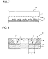
- Fig. 7 is a sectional view showing a structure example of a liquid crystal display 20 having a backlight applying the light-emitting device 1.
- the liquid crystal display 20 is provided with a flat liquid crystal panel 21 as, for example, a flat display means and a backlight 22 which illuminates the liquid crystal panel 21 from its back.
- the backlight 22 is arranged directly beneath the liquid crystal panel 21.
- the liquid crystal panel 21 has an array substrate and a color filter substrate, which are glass plates having transparent electrodes formed thereon, disposed to face each other between two polarizing plates. Liquid crystal is filled between the array substrate and the color filter substrate to form a liquid crystal layer. Red (R), green (G) and blue (B) color filters are formed in correspondence with individual pixels on the color filter substrate.
- the backlight 22 is provided with a mounting substrate (base substrate) 23 and the plural light-emitting devices 1 which are arranged and mounted in a matrix form on the mounting substrate 23.
- the specific module structure is as follows.
- the plural light-emitting devices 1 configure the light source of the backlight 22.
- the light-emitting devices 1 are arranged such that the non-light emission surfaces are positioned on the side of the mounting substrate 23.
- An optical sheet 24 such as a diffuser sheet, a prism sheet or the like is arranged on the side of the light emission surfaces 10 of the light-emitting devices 1.
- the backlight 22 is arranged directly beneath the liquid crystal panel 21 such that the optical sheet 24 is positioned on the side of the liquid crystal panel 21.
- the liquid crystal display of the present invention is not limited to one using the directly-beneath type backlight but may apply a side-light type backlight.
- the side-light type backlight has, for example, a light source with the plural light-emitting devices 1 arranged linearly and a light guide plate.
- the light source is disposed at a light incident portion which is disposed at one end surface of the light guide plate. Light having entered through the light incident portion repeats refraction and reflection within the light guide plate and is irradiated from the top surface of the light guide plate in a direction of its normal line.
- the liquid crystal display section is arranged on the side of the top surface (light emission surface) of the light guide plate.
- the reflector 5 was used in plural types such that its distance (L) to the UV-LED element 4 fell in a range of 0.6 to 1.4 mm (Examples 1 through 5).
- the UV-LED element 4 and the reflector 5 was electrically connected by a conductive wire 6, and a phosphor paste which had a mixture of a red phosphor, a green phosphor and a blue phosphor to be excited by ultraviolet rays dispersed into a transparent resin was filled in the reflector 5 and cured by heating to produce a white light-emitting device 1.
- a white light-emitting device 30 shown in Fig. 8 was produced.
- an aluminum nitride substrate 32 (5 mm long x 5 mm wide x 0.5 mm thick), on which terminal metal fittings 31 shown in Fig. 8 were disposed, was prepared.
- a UV-LED element 33 was bonded to a prescribed portion of the aluminum nitride substrate 32, and a reflector 35 (1 mm high, reflecting surface angle ( ⁇ ) 45°) formed of silver-plated oxygen-free copper was bonded to a reflecting surface 34.
- individual electrodes of the UV-LED element 33 and the individual terminal metal fittings 31 were electrically connected by conductive wires 36.
- a phosphor paste which had a mixture of a red phosphor, a green phosphor and a blue phosphor to be excited by ultraviolet rays dispersed into a transparent resin was filled in the reflector 35 and cured by heating to produce the white light-emitting device 30.
- the white light-emitting device 30 was determined to have the distance (L) of 1.8 mm between the UV-LED element 33 and the reflector 35 in order to secure the connection points between the conductive wires 36 and the terminal metal fittings 31.
- the white light-emitting device 30 of Comparative Example 1 which has the conductive wires 36 arranged on the aluminum nitride substrate 32 between the UV-LED element 33 and the reflector 35 requires to secure the connection points between the conductive wires 36 and the terminal metal fittings 31, so that the distance (L) between the UV-LED element 33 and the reflector 35 becomes large. Therefore, it was confirmed that light emitted from the UV-LED element 33 tends to be diffused by the phosphor contained in a light-emitting portion 37 before it reaches the reflecting surface 34 of the reflector 35, and a total luminous flux becomes small as a result.
- the light-emitting devices 1 of Examples 1 through 5 using the internal wiring 2 of the aluminum nitride substrate 3 as the electrical conduction to the UV-LED element 4 and the reflector 5 can decrease the distance (L) between the UV-LED element 4 and the reflector 5. Therefore, the light emitted from the UV-LED element 4 is suppressed from being diffused needlessly by the phosphor contained in the light-emitting portion 7 before it reaches the reflecting surface 9 of the reflector 5. Thus, it was confirmed that a total luminous flux was improved. Especially, it was confirmed that a total luminous flux was improved greatly when the distance (L) between the UV-LED element 4 and the reflector 5 was determined to be 1 mm or less.
- the uneven luminance was visually observed on the light emission surfaces of the directly-beneath type backlights and evaluated depending on a degree of appearance that the light of the white light-emitting device 1 was seen as a dot.
- Table 2 “A” indicates that no part was seen as a dot, “B” indicates that some parts were seen as a dot, and “C” indicates that many parts were seen as a dot.
- the emission luminance the light emission surfaces of the directly-beneath type backlights were visually observed. And, “A” indicates that the emission luminance of the directly-beneath type backlight is sufficient, and “B” indicates that the emission luminance is somewhat insufficient.
- the white light-emitting device 1 used for the directly-beneath type backlight is desired to have the angle ( ⁇ ) of the reflecting surface 9 of the reflector 5 determined to be 35° or more and 45° or less from viewpoints of the suppression of the uneven luminance and the improvement of the emission luminance.
- the side light type backlights were evaluated for the presence or not of the uneven luminance and the emission luminance. The obtained results are shown in Table 3.
- the uneven luminance and the emission luminance were evaluated in the same manner as in Examples 6 through 10.
- the side light type backlights each were produced with the ten white light-emitting devices uniformly arranged at equal intervals.
- the side light type backlight has no occurrence of uneven luminance regardless of the angle ( ⁇ ) of the reflecting surface 9 of the reflector 5 of the white light-emitting device 1. Since the side light type backlight uses the light guide plate, the occurrence of uneven luminance is suppressed regardless of the angle ( ⁇ ) of the reflecting surface 9 of the reflector 5 of the white light-emitting device 1. It was confirmed that when the angle ( ⁇ ) of the reflecting surface 9 of the reflector 5 was determined to be less than 35°, the emission luminance was degraded. It is seen that the white light-emitting device 1 used for the side light type backlight is desired to have the angle ( ⁇ ) of the reflecting surface 9 of the reflector 5 determined to be 35° or more.
- the light-emitting device can irradiate light, which is emitted from the semiconductor light-emitting element, to the reflector without diffusing needlessly within the light-emitting portion, so that excellent emission luminance can be obtained.
- the productivity and reliability of the light-emitting device can be enhanced.
- Such a light-emitting device is effectively used for various lighting usages such as a backlight.
Landscapes
- Led Device Packages (AREA)
- Planar Illumination Modules (AREA)
Applications Claiming Priority (2)
| Application Number | Priority Date | Filing Date | Title |
|---|---|---|---|
| JP2005241692 | 2005-08-23 | ||
| PCT/JP2006/316400 WO2007023807A1 (ja) | 2005-08-23 | 2006-08-22 | 発光装置とそれを用いたバックライトおよび液晶表示装置 |
Publications (3)
| Publication Number | Publication Date |
|---|---|
| EP1919002A1 true EP1919002A1 (de) | 2008-05-07 |
| EP1919002A4 EP1919002A4 (de) | 2011-01-12 |
| EP1919002B1 EP1919002B1 (de) | 2018-07-18 |
Family
ID=37771550
Family Applications (1)
| Application Number | Title | Priority Date | Filing Date |
|---|---|---|---|
| EP06796614.3A Not-in-force EP1919002B1 (de) | 2005-08-23 | 2006-08-22 | Lichtemittierende vorrichtung, rückbeleuchtung damit und flüssigkristallanzeige |
Country Status (7)
| Country | Link |
|---|---|
| US (1) | US7709855B2 (de) |
| EP (1) | EP1919002B1 (de) |
| JP (1) | JPWO2007023807A1 (de) |
| KR (1) | KR20080037734A (de) |
| CN (1) | CN101248533B (de) |
| TW (1) | TW200727045A (de) |
| WO (1) | WO2007023807A1 (de) |
Cited By (3)
| Publication number | Priority date | Publication date | Assignee | Title |
|---|---|---|---|---|
| WO2015114477A1 (en) * | 2014-01-29 | 2015-08-06 | Koninklijke Philips N.V. | Shallow reflector cup for phosphor-converted led filled with encapsulant |
| WO2020185866A1 (en) * | 2019-03-11 | 2020-09-17 | Lumileds Llc | Light extraction bridge in cups |
| US11112652B2 (en) | 2018-12-11 | 2021-09-07 | Lg Display Co., Ltd. | Backlight unit and display device including the same technical field |
Families Citing this family (26)
| Publication number | Priority date | Publication date | Assignee | Title |
|---|---|---|---|---|
| JP5441316B2 (ja) * | 2007-04-05 | 2014-03-12 | ローム株式会社 | 半導体発光装置 |
| US8487525B2 (en) | 2007-05-04 | 2013-07-16 | Seoul Semiconductor Co., Ltd. | Light emitting device including optical lens |
| JP2008300573A (ja) * | 2007-05-30 | 2008-12-11 | Toshiba Corp | 発光装置 |
| JP5151301B2 (ja) * | 2007-08-06 | 2013-02-27 | 日亜化学工業株式会社 | 半導体発光素子及びその製造方法 |
| JP4381439B2 (ja) * | 2007-09-18 | 2009-12-09 | 株式会社沖データ | Ledバックライト装置及び液晶表示装置 |
| JP5277610B2 (ja) * | 2007-10-29 | 2013-08-28 | 日亜化学工業株式会社 | 発光装置及び面発光装置並びに発光装置用パッケージ |
| JP4968014B2 (ja) * | 2007-11-22 | 2012-07-04 | ソニー株式会社 | バックライト装置及び液晶表示装置 |
| JP5056372B2 (ja) * | 2007-11-22 | 2012-10-24 | ソニー株式会社 | バックライト装置及び液晶表示装置 |
| JP5064278B2 (ja) * | 2008-03-25 | 2012-10-31 | 日東電工株式会社 | 光半導体素子封止用樹脂シートおよび光半導体装置 |
| KR101406787B1 (ko) * | 2008-06-24 | 2014-06-12 | 삼성전자주식회사 | Led 패키지 |
| JP2010171379A (ja) * | 2008-12-25 | 2010-08-05 | Seiko Instruments Inc | 発光デバイス |
| JP5343831B2 (ja) * | 2009-04-16 | 2013-11-13 | 日亜化学工業株式会社 | 発光装置 |
| KR100939304B1 (ko) * | 2009-06-18 | 2010-01-28 | 유트로닉스주식회사 | Led어레이모듈 및 그 제조방법 |
| KR101186648B1 (ko) * | 2009-12-21 | 2012-09-28 | 서울반도체 주식회사 | Led 패키지 및 그의 제조 방법 |
| KR101055081B1 (ko) * | 2010-01-15 | 2011-08-08 | 엘지이노텍 주식회사 | 발광 소자, 발광 소자 제조방법 및 백라이트 유닛 |
| DE102010025319B4 (de) * | 2010-06-28 | 2022-05-25 | OSRAM Opto Semiconductors Gesellschaft mit beschränkter Haftung | Verfahren zur Herstellung eines oberflächenmontierbaren Halbleiterbauelements und oberflächenmontierbare Halbleiterbauelemente |
| JP2012054460A (ja) * | 2010-09-02 | 2012-03-15 | Citizen Electronics Co Ltd | 半導体発光装置 |
| KR101142152B1 (ko) | 2011-02-01 | 2012-05-21 | 서울대학교산학협력단 | 긴 소수성 사슬이 도입된 리간드로 코팅된 나노입자 및 이의 제조방법 |
| US8382333B2 (en) * | 2011-06-03 | 2013-02-26 | Kuei-Fang Chen | Light emitting device |
| JP6282419B2 (ja) * | 2012-07-27 | 2018-02-21 | エルジー イノテック カンパニー リミテッド | 照明装置 |
| JP6135721B2 (ja) * | 2015-08-10 | 2017-05-31 | 大日本印刷株式会社 | 樹脂付リードフレームおよびその製造方法、ならびに半導体装置およびその製造方法 |
| JP6283013B2 (ja) * | 2015-11-24 | 2018-02-21 | カルソニックカンセイ株式会社 | 照明構造 |
| CN110794614B (zh) * | 2018-08-03 | 2022-10-25 | 日亚化学工业株式会社 | 发光模块 |
| KR102736892B1 (ko) * | 2018-12-06 | 2024-12-03 | 엘지디스플레이 주식회사 | 백라이트 유닛 및 디스플레이 장치 |
| KR102736900B1 (ko) * | 2018-12-11 | 2024-12-03 | 엘지디스플레이 주식회사 | 백라이트 유닛 및 그를 포함하는 표시장치 |
| KR102564142B1 (ko) * | 2019-07-03 | 2023-08-07 | 엘지디스플레이 주식회사 | 백라이트 유닛 및 그를 포함하는 표시장치 |
Family Cites Families (29)
| Publication number | Priority date | Publication date | Assignee | Title |
|---|---|---|---|---|
| TW383508B (en) | 1996-07-29 | 2000-03-01 | Nichia Kagaku Kogyo Kk | Light emitting device and display |
| JP2000277813A (ja) * | 1999-03-26 | 2000-10-06 | Matsushita Electric Works Ltd | 光源装置 |
| JP3696021B2 (ja) * | 2000-01-20 | 2005-09-14 | 三洋電機株式会社 | 光照射装置 |
| JP2001210122A (ja) | 2000-01-28 | 2001-08-03 | Matsushita Electric Ind Co Ltd | 照明装置、映像表示装置、映像表示装置の駆動方法、液晶表示パネル、液晶表示パネルの製造方法、液晶表示パネルの駆動方法、アレイ基板、表示装置、ビューファインダおよびビデオカメラ |
| JP2001267637A (ja) * | 2000-03-15 | 2001-09-28 | Nippon Aleph Corp | 発光装置 |
| JP2001332760A (ja) * | 2000-05-25 | 2001-11-30 | Toyoda Gosei Co Ltd | Iii族窒化物系化合物半導体発光素子 |
| JP4737842B2 (ja) | 2001-01-30 | 2011-08-03 | 京セラ株式会社 | 発光素子収納用パッケージの製造方法 |
| JP3844196B2 (ja) * | 2001-06-12 | 2006-11-08 | シチズン電子株式会社 | 発光ダイオードの製造方法 |
| US6531328B1 (en) * | 2001-10-11 | 2003-03-11 | Solidlite Corporation | Packaging of light-emitting diode |
| JP2003160785A (ja) | 2001-11-27 | 2003-06-06 | Toshiba Corp | 赤色発光蛍光体とそれを用いた発光装置 |
| US7429757B2 (en) * | 2002-06-19 | 2008-09-30 | Sanken Electric Co., Ltd. | Semiconductor light emitting device capable of increasing its brightness |
| JP4542329B2 (ja) | 2002-11-25 | 2010-09-15 | パナソニック株式会社 | Led照明光源 |
| CN100352069C (zh) * | 2002-11-25 | 2007-11-28 | 松下电器产业株式会社 | Led照明光源 |
| JP3948417B2 (ja) * | 2003-02-28 | 2007-07-25 | ノーリツ鋼機株式会社 | 光源ユニット |
| US7518155B2 (en) * | 2003-03-18 | 2009-04-14 | Sumitomo Electric Industries, Ltd. | Light emitting element mounting member, and semiconductor device using the same |
| US7095053B2 (en) * | 2003-05-05 | 2006-08-22 | Lamina Ceramics, Inc. | Light emitting diodes packaged for high temperature operation |
| US7528421B2 (en) * | 2003-05-05 | 2009-05-05 | Lamina Lighting, Inc. | Surface mountable light emitting diode assemblies packaged for high temperature operation |
| US7495322B2 (en) * | 2003-05-26 | 2009-02-24 | Panasonic Electric Works Co., Ltd. | Light-emitting device |
| JP4238980B2 (ja) * | 2003-06-05 | 2009-03-18 | 株式会社ファインラバー研究所 | 赤色発光蛍光体及び発光装置 |
| DE602004020906D1 (de) * | 2003-09-19 | 2009-06-10 | Panasonic Corp | Beleuchtungseinrichtung |
| JP4206334B2 (ja) | 2003-12-25 | 2009-01-07 | 京セラ株式会社 | 発光装置 |
| KR100586944B1 (ko) * | 2003-12-26 | 2006-06-07 | 삼성전기주식회사 | 고출력 발광다이오드 패키지 및 제조방법 |
| JP2005223222A (ja) * | 2004-02-06 | 2005-08-18 | Toyoda Gosei Co Ltd | 固体素子パッケージ |
| JP2006012868A (ja) * | 2004-06-22 | 2006-01-12 | Toshiba Corp | 半導体発光素子用パッケージおよびそれを用いた半導体発光装置 |
| DE102004031391B4 (de) * | 2004-06-29 | 2009-06-04 | Osram Opto Semiconductors Gmbh | Elektronisches Bauteil mit Gehäuse zum ESD-Schutz |
| JP2006134975A (ja) * | 2004-11-04 | 2006-05-25 | Hitachi Displays Ltd | 照明装置及びこの照明装置を用いた表示装置 |
| JP4711715B2 (ja) * | 2005-03-30 | 2011-06-29 | 株式会社東芝 | 半導体発光装置及び半導体発光ユニット |
| KR100703218B1 (ko) * | 2006-03-14 | 2007-04-09 | 삼성전기주식회사 | 발광다이오드 패키지 |
| KR100735310B1 (ko) * | 2006-04-21 | 2007-07-04 | 삼성전기주식회사 | 다층 반사 면 구조를 갖는 엘이디 패키지 및 그 제조방법 |
-
2006
- 2006-08-22 JP JP2007532123A patent/JPWO2007023807A1/ja active Pending
- 2006-08-22 CN CN2006800300476A patent/CN101248533B/zh not_active Expired - Fee Related
- 2006-08-22 WO PCT/JP2006/316400 patent/WO2007023807A1/ja not_active Ceased
- 2006-08-22 KR KR1020087006952A patent/KR20080037734A/ko not_active Ceased
- 2006-08-22 US US12/064,519 patent/US7709855B2/en not_active Expired - Fee Related
- 2006-08-22 EP EP06796614.3A patent/EP1919002B1/de not_active Not-in-force
- 2006-08-23 TW TW095131003A patent/TW200727045A/zh not_active IP Right Cessation
Cited By (8)
| Publication number | Priority date | Publication date | Assignee | Title |
|---|---|---|---|---|
| WO2015114477A1 (en) * | 2014-01-29 | 2015-08-06 | Koninklijke Philips N.V. | Shallow reflector cup for phosphor-converted led filled with encapsulant |
| US9634208B2 (en) | 2014-01-29 | 2017-04-25 | Koninklijke Philips N.V. | Shallow reflector cup for phosphor-converted LED filled with encapsulant |
| US10062819B2 (en) | 2014-01-29 | 2018-08-28 | Lumileds Llc | Shallow reflector cup for phosphor-converted LED filled with encapsulant |
| US11112652B2 (en) | 2018-12-11 | 2021-09-07 | Lg Display Co., Ltd. | Backlight unit and display device including the same technical field |
| GB2581420B (en) * | 2018-12-11 | 2021-10-13 | Lg Display Co Ltd | Backlight unit and display device including the same |
| WO2020185866A1 (en) * | 2019-03-11 | 2020-09-17 | Lumileds Llc | Light extraction bridge in cups |
| US11092311B2 (en) | 2019-03-11 | 2021-08-17 | Lumileds Llc | Light extraction bridge in cups |
| KR20210128011A (ko) * | 2019-03-11 | 2021-10-25 | 루미레즈 엘엘씨 | 컵들 내의 광 추출 브리지 |
Also Published As
| Publication number | Publication date |
|---|---|
| US7709855B2 (en) | 2010-05-04 |
| US20090097233A1 (en) | 2009-04-16 |
| EP1919002A4 (de) | 2011-01-12 |
| CN101248533B (zh) | 2010-06-02 |
| EP1919002B1 (de) | 2018-07-18 |
| JPWO2007023807A1 (ja) | 2009-02-26 |
| KR20080037734A (ko) | 2008-04-30 |
| CN101248533A (zh) | 2008-08-20 |
| TW200727045A (en) | 2007-07-16 |
| TWI345109B (de) | 2011-07-11 |
| WO2007023807A1 (ja) | 2007-03-01 |
Similar Documents
| Publication | Publication Date | Title |
|---|---|---|
| EP1919002B1 (de) | Lichtemittierende vorrichtung, rückbeleuchtung damit und flüssigkristallanzeige | |
| EP1271664B1 (de) | Lichtemittierende Vorrichtung | |
| US7078737B2 (en) | Light-emitting device | |
| EP1840977A1 (de) | Lichtquelle und beleuchtungseinrichtung | |
| KR100958759B1 (ko) | 백라이트와 그것을 이용한 액정 표시 장치 | |
| EP2445020B1 (de) | Leuchtdioden-Gehäuse | |
| KR102098318B1 (ko) | 형광체 및 이를 구비한 발광 소자 | |
| HK1144978B (en) | Light emitting device and display | |
| HK1144982B (en) | Light-emitting device | |
| HK1027668B (en) | Method of preparing a white light emitting device | |
| HK1144979B (en) | Light emitting device and display | |
| HK1149851B (en) | Light emitting device and display | |
| HK1144980B (en) | Light emitting device and display |
Legal Events
| Date | Code | Title | Description |
|---|---|---|---|
| PUAI | Public reference made under article 153(3) epc to a published international application that has entered the european phase |
Free format text: ORIGINAL CODE: 0009012 |
|
| 17P | Request for examination filed |
Effective date: 20080218 |
|
| AK | Designated contracting states |
Kind code of ref document: A1 Designated state(s): DE NL |
|
| RBV | Designated contracting states (corrected) |
Designated state(s): DE NL |
|
| A4 | Supplementary search report drawn up and despatched |
Effective date: 20101213 |
|
| DAX | Request for extension of the european patent (deleted) | ||
| 17Q | First examination report despatched |
Effective date: 20131121 |
|
| REG | Reference to a national code |
Ref country code: DE Ref legal event code: R079 Ref document number: 602006055859 Country of ref document: DE Free format text: PREVIOUS MAIN CLASS: H01L0033000000 Ipc: H01L0033620000 |
|
| RIC1 | Information provided on ipc code assigned before grant |
Ipc: H01L 33/60 20100101ALI20171221BHEP Ipc: H01L 33/62 20100101AFI20171221BHEP |
|
| GRAP | Despatch of communication of intention to grant a patent |
Free format text: ORIGINAL CODE: EPIDOSNIGR1 |
|
| STAA | Information on the status of an ep patent application or granted ep patent |
Free format text: STATUS: GRANT OF PATENT IS INTENDED |
|
| INTG | Intention to grant announced |
Effective date: 20180129 |
|
| GRAS | Grant fee paid |
Free format text: ORIGINAL CODE: EPIDOSNIGR3 |
|
| GRAA | (expected) grant |
Free format text: ORIGINAL CODE: 0009210 |
|
| STAA | Information on the status of an ep patent application or granted ep patent |
Free format text: STATUS: THE PATENT HAS BEEN GRANTED |
|
| AK | Designated contracting states |
Kind code of ref document: B1 Designated state(s): DE NL |
|
| REG | Reference to a national code |
Ref country code: DE Ref legal event code: R096 Ref document number: 602006055859 Country of ref document: DE |
|
| REG | Reference to a national code |
Ref country code: NL Ref legal event code: MP Effective date: 20180718 |
|
| PG25 | Lapsed in a contracting state [announced via postgrant information from national office to epo] |
Ref country code: NL Free format text: LAPSE BECAUSE OF FAILURE TO SUBMIT A TRANSLATION OF THE DESCRIPTION OR TO PAY THE FEE WITHIN THE PRESCRIBED TIME-LIMIT Effective date: 20180718 |
|
| RIC2 | Information provided on ipc code assigned after grant |
Ipc: H01L 33/60 20100101ALI20171221BHEP Ipc: H01L 33/62 20100101AFI20171221BHEP |
|
| REG | Reference to a national code |
Ref country code: DE Ref legal event code: R097 Ref document number: 602006055859 Country of ref document: DE |
|
| PLBE | No opposition filed within time limit |
Free format text: ORIGINAL CODE: 0009261 |
|
| STAA | Information on the status of an ep patent application or granted ep patent |
Free format text: STATUS: NO OPPOSITION FILED WITHIN TIME LIMIT |
|
| 26N | No opposition filed |
Effective date: 20190423 |
|
| PGFP | Annual fee paid to national office [announced via postgrant information from national office to epo] |
Ref country code: DE Payment date: 20210713 Year of fee payment: 16 |
|
| REG | Reference to a national code |
Ref country code: DE Ref legal event code: R119 Ref document number: 602006055859 Country of ref document: DE |
|
| PG25 | Lapsed in a contracting state [announced via postgrant information from national office to epo] |
Ref country code: DE Free format text: LAPSE BECAUSE OF NON-PAYMENT OF DUE FEES Effective date: 20230301 |