EP1919024A1 - Vorrichtung zur Ausbreitung elektromagnetischer Wellen mit modulierter Dielektrizitätskonstante - Google Patents
Vorrichtung zur Ausbreitung elektromagnetischer Wellen mit modulierter Dielektrizitätskonstante Download PDFInfo
- Publication number
- EP1919024A1 EP1919024A1 EP07021125A EP07021125A EP1919024A1 EP 1919024 A1 EP1919024 A1 EP 1919024A1 EP 07021125 A EP07021125 A EP 07021125A EP 07021125 A EP07021125 A EP 07021125A EP 1919024 A1 EP1919024 A1 EP 1919024A1
- Authority
- EP
- European Patent Office
- Prior art keywords
- conductive layer
- propagation
- electromagnetic waves
- dielectric constant
- width
- Prior art date
- Legal status (The legal status is an assumption and is not a legal conclusion. Google has not performed a legal analysis and makes no representation as to the accuracy of the status listed.)
- Granted
Links
Images



Classifications
-
- H—ELECTRICITY
- H01—ELECTRIC ELEMENTS
- H01P—WAVEGUIDES; RESONATORS, LINES, OR OTHER DEVICES OF THE WAVEGUIDE TYPE
- H01P1/00—Auxiliary devices
- H01P1/20—Frequency-selective devices, e.g. filters
- H01P1/201—Filters for transverse electromagnetic waves
- H01P1/203—Strip line filters
-
- H—ELECTRICITY
- H01—ELECTRIC ELEMENTS
- H01P—WAVEGUIDES; RESONATORS, LINES, OR OTHER DEVICES OF THE WAVEGUIDE TYPE
- H01P3/00—Waveguides; Transmission lines of the waveguide type
- H01P3/02—Waveguides; Transmission lines of the waveguide type with two longitudinal conductors
- H01P3/08—Microstrips; Strip lines
Definitions
- the present invention relates to the field of electromagnetic wave propagation. More in detail, the present invention relates to the propagation of electromagnetic waves through a microstrip structure with a dielectric constant which varies inside the structure.
- the present invention relates to a device which is used as support for the propagation of electromagnetic waves and which comprises a layer of dielectric material and at least one conductive layer or conductive track, in which the relative dielectric constant of the device is modulated by the shape of said conductive layer or conductive track. More in detail, the present invention is related to a device suited for the propagation of electromagnetic waves where the electric constant is periodically modulated along a predetermined direction by a periodic variation of the shape of said conductive layer along the same predetermined direction.
- the present invention relates to a device which is suited for the propagation of electromagnetic waves whose effective dielectric constant is sinusoidally modulated along a predetermined direction by a periodic variation of the shape of said conductive layer along the same direction.
- Said periodic and/or sinusoidal variation can regard the width of said conductive layer, its thickness, or both of these characteristics.
- EBG materials electromagnetic band gap structures
- the materials are selective in frequency and therefore allow the propagation of electromagnetic waves of a given frequency while blocking the propagation of waves with other frequencies.
- This phenomenon presents strong similarities with the band structure of materials with a crystalline structure.
- materials such as semiconductors which have a band energy structure such that an electron can have only energy values which correspond to an allowed energy band, while it cannot have values which correspond to a forbidden band.
- the EBG materials allow the propagation of electromagnetic waves with frequencies comprised within given bands or intervals while they block the wave propagation of waves with frequencies outside said bands or intervals.
- EBG materials have become widely employed in antenna applications, as for example leaky wave antennas, lens antennas or also surface wave coupling reduction between antennas, etc. (see for example: Fan, Y.; Rahmat-Samii, Y.; "Microstrip antennas integrated with electromagnetic band-gap (EBG) structures: low mutual coupling design for array applications", IEEE Trans. AP, pgs 2936-2946, October 2003 ).
- EBG electromagnetic band-gap
- the EBG behavior can be obtained in different ways, for example by arranging reactive loads, with concentrated or distributed parameters, which are smaller than the wavelength of the wave that propagates in the device or by modulation of the media electromagnetic properties.
- modulation of the electromagnetic properties of a structure can be obtained using different techniques, such as for example the modulation of its physical characteristics, that is placing materials with different dielectric constants side-by-side or one on top of another or by using electro-optic materials, materials which change their dielectric properties under the application of electromagnetic fields.
- the modulation of the parameters of the material can be achieved by drilling holes in the dielectric material.
- a complete characterization of EBG material can be carried out by a dispersion diagram, which represents the wavenumber in function of the frequency of the electromagnetic waves (see for example: Brillouin, L. "Wave Propagation in periodic structures", New York: Dover, 1953 ).
- the drilling techniques (with or without metallization) have proved not to be suited for the microstructures which are required by the demand for ever greater scale reduction of circuits and/or devices; in fact, it has proved very difficult, if not impossible, to realize microholes with dimensions suited for today's circuits such as integrated circuits or the like.
- the object of the present invention is to obtain structures or materials suited to the propagation of electromagnetic waves which present a stable EBG behavior and which are not influenced by environmental factors; furthermore, said materials and/or structures can be realized at competitive costs and present dimensions suited to the demand for an always greater miniaturization of devices and/or circuits in general.
- the proposed structure as it does not present any holes, is easier to realize with lower costs. For the same reason, it also presents a larger mechanical resistance.
- the substrate can be multilayer, meaning that the conductive layer is located in a multilayer structure made of dielectric materials with different relative dielectric constants.
- the conductive layer is located closer to the interface with the air, but not necessarily at the interface air-dielectric; this solution allows to have an M value (modulation factor) which allows control over the position and the width of the forbidden bands.
- the present invention is based on the consideration that a device and/or structure suited for the propagation of electromagnetic waves and which presents an EBG behavior can be obtained by modulation of at least one of the electromagnetic properties of said structure and/or device. Furthermore, the present invention is based on the consideration that the EBG behavior can be obtained by modulation of the effective dielectric constant of the structure or device. Particularly, the present invention is based on the consideration that an appropriate modulation of the dielectric constant of the structure or device, one that provides an EBG behavior, can be obtained by realizing a conductive layer whose shape and/or dimensions are not constant but vary along a predetermined direction so as to modulate the effective dielectric constant of the structure and/or device along said direction and said predefined profile.
- the present invention relates to a device as claimed in main claim 1. That is, a device suited for the propagation of electromagnetic waves and comprising a conductive mass plate, a substrate, and at least one other conductive layer in which at least one electromagnetic property of said device is modulated in a periodic way within said device by said conductive layer.
- the effective dielectric constant of the device is modulated by the shape of said at least one conductive layer.
- the width of said at least one conductive layer varies in a substantially periodic way along a predetermined direction, so that said dielectric constant is periodically modulated along said predetermined direction.
- the width of said at least one conductive layer varies substantially sinusoidally along said predetermined direction, so that said effective dielectric constant is modulated according to a substantially sinusoidal profile along said predetermined direction.
- one possible way to confer an EBG behavior to a structure suited for the propagation and/or transmission of electromagnetic waves is to modulate the effective dielectric constant, for example following a periodic profile, in particular a sinusoidal profile.
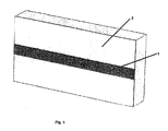
- microstrip structure as represented in Figure 1, which comprises a thin and flat electric conductor 1 separated from a mass plate (not shown in Figure 1) by a dielectric material 2, the following consideration may be made.
- Microstrip structures of this type are widely used as transmission lines for microwaves.
- the electromagnetic waves which propagate in a microstrip structure of this kind diffuse in part in the dielectric material and in part in the air.
- the propagation velocity of the electromagnetic waves corresponds therefore to a value which is comprised between the propagation wave velocity in the dielectric and the propagation velocity in the air.
- the microstrip structure is therefore characterized by an effective dielectric constant ⁇ eff which is given by the formula (for details Hammerstad, E. and Jensen, O., "Accurate Models for Microstrip Computer-Aided Design", Digest of 1980 IEEE MTT-S International Symposium, Washington D.
- ⁇ eff ⁇ r + 1 2 + ⁇ r - 1 2 ⁇ 1 + 10 ⁇ h w - 0.5 in which ⁇ r is the dielectric constant of the dielectric material, h is the thickness of the dielectric material and w is the width of the conductive layer.
- ⁇ r is the dielectric constant of the dielectric material
- h is the thickness of the dielectric material
- w is the width of the conductive layer.
- the inventors faced therefore the problem of determining the behavior of a microstrip structure of the type represented in Figure 2, in which the conductive layer 2 does not have a constant width along the propagation direction of the electromagnetic waves, and they arrived at the conclusion that, as previously shown, the effective dielectric constant of a microstrip structure depends on the width of the conductive layer. By varying this width it is possible to modulate the value of the effective dielectric constant along the propagation direction.
- the inventors arrived therefore at the unexpected conclusion that in this way it is possible to obtain a microstrip structure with new electromagnetic properties, which can bring considerable advantages in many applications.
- the modulation of the effective dielectric constant can allow the structure to block certain wavelengths and let others propagate through, acting therefore as a filter.
- M is a real value, which corresponds to the case without absorption of the electromagnetic wave by the structure.
- the effective dielectric constant becomes complex, which corresponds for example to the heat dissipation by the Joule effect in the dielectric material.
- the effective dielectric constant varies only in the propagation direction of the electromagnetic waves.
- transversal electric field TE
- TM transversal magnetic field
- the transversal magnetic field can be obtained analytically by means of the Hill functions, while the transversal electric field can be obtained in terms of the Mathieu functions, which are a particular case of the Hill functions.
- the limits of the bands which allow the propagation of the electromagnetic waves or stop the electromagnetic waves, can be obtained by the intersection between the line which corresponds to the modulation parameters and the limits of the stability zones of these functions.
- the behavior inside the band is described by the relative functions of non-integer order.
- a microstrip structure with a unique conductive layer in which the effective dielectric constant varies is considered.
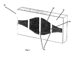
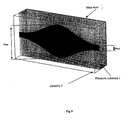
- Figure 2 schematically illustrates a period of a particular embodiment of the present invention in which the structure 20 comprises a dielectric substrate 21 on whose surface is disposed a conductive layer 22.
- the conductive layer 22 extends longitudinally along the entire length of the substrate 21 as shown in Figure 2.
- the electromagnetic waves propagate inside the structure represented in Figure 2 along the direction in which the conductive layer extends longitudinally. In the following, this propagation direction will be defined as the predetermined or predefined direction.
- the shape of the conductive layer and in particular its width varies periodically according to a function which results from the equation (3).
- the structure 30 comprises a dielectric substrate 31 on whose surface is disposed a non-continuous conductive layer 32.
- the conductive layer 32 extends longitudinally along the entire length of the substrate 31 and it is interrupted by non-conductive strips/zones 33 as shown in Figure 3.
- the conductive layer 32 is therefore made up of conductive and non-conductive strips.
- the length in the predefined longitudinal direction of both the conductive and non-conductive strips is constant along all the substrate.
- the width (measured in the transversal direction) of the conductive strips is variable and it describes a periodic profile as shown in Figure 3.
- the length in the longitudinal direction of the non-conductive strips is identified by the reference number 33 and in a further particular embodiment of the present invention said length has a value of 0.2 mm.
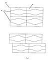
- Figure 6 schematically illustrates a further particular embodiment of the present invention in which the bi-dimensional structure 60 comprises a dielectric substrate 61 on whose surface are disposed a plurality of conductive layers 62.
- the conductive layers are parallel and there is no contact between the different conductive layers as shown in Figure 6.
- the conductive layer 62 extends longitudinally along the entire length of the substrate 61 as shown in Figure 6.
- the different conductive layers have a periodic profile which is substantially sinusoidal and are in phase with one another as shown in the upper part of Figure 6.
- the expression "in phase” it should be understood that the functions of the width of the two conductive adjacent layers which are periodical along the predefined longitudinal direction are in phase between them (at a given value u corresponds the same value of w).
- the conductive layers can be out of phase, as shown in the lower part of Figure 6.
- the functions that express the periodicity along the predefined longitudinal direction of the width of the 2 adjacent conductive layers are out of phase (at a given value of u correspond different values of w).
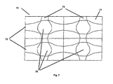
- Figure 7 schematically shows a particular embodiment of the present invention in which the two dimensional structure 70 comprises a dielectric substrate 71 on whose surface are disposed conductive longitudinal layers 72 and conductive transversal layers 73.
- the longitudinal conductive layers are parallel and there is no contact between them, as shown in Figure 7. The same is valid for the transversal conductive layers.
- the longitudinal conductive layers come into contact with their respective transversal layers in the contact points 74.
- Both the longitudinal 72 and transversal 73 conductive layers extend respectively longitudinally and transversally for the entire length/width of the dielectric substrate 71.
- the conductive layers therefore form a radical structure on the dielectric surface 71.
- the electromagnetic waves can propagate in both the longitudinal and transversal directions.
- the dielectric material 2 is made of Arlon 350 with a thickness of 1.58 mm and the conductive layer 11 is made of copper with a thickness of 35 ⁇ m as is the mass layer behind.
- the modulation of the effective dielectric constant takes place in a continuous way in one dimension (1 D) thanks to a continuous conductive layer, as shown in Figure 2, whose width varies periodically and/or substantially sinusoidally.
- the conductive layer is not continuous and it is interrupted by non-conductive zones, that is it is made of conductive strips alternated with non-conductive zones.
- the width of the conductive strips is not constant.
- the width of the strips varies in a periodic way and/or sinusoidal way according to the profile of equation (3) as shown in Figure 3.
- the distance between the different conductive strips is smaller than the wavelength of the electromagnetic waves which propagates in the microstrip structure.
- the frequency of the electromagnetic waves employed is within the range of 0 to 25 GHz.
- the width of the conductive layer varies between a minimum of 0.70 mm and a maximum of 3.50 mm on a period of 10 mm.
- the conductive layer is not continuous and it is interrupted by cuts which have a width of 0.2 mm.
- a plurality of conductive layers are disposed on the dielectric substrate as shown in Figure 6.
- the different conductive layers are disposed on the same plane and are parallel to each other.
- the particular shapes of the conductive layers can be in phase as shown in the upper part of Figure 6 or they can be disposed out of phase as shown in the lower part of the same figure.
- the conductive layers which are disposed on the dielectric substrate can come into contact forming therefore a two-dimensional conductive lattice as shown in Figure 7.
- These two-dimensional embodiments according to the present invention can be employed as a substrate to reduce cross-talk between data transmission lines. Actually, this is the most widely employed application. Furthermore, reducing the coupling means that the lines can be placed closer to each other and therefore the dimensions of the entire circuit can be reduced with an important advantage in terms of costs, volume, etc.
- the modulation of the effective dielectric constant can be obtained by varying the thickness of the conductive layer instead of the width as mentioned in the previous embodiments.
- the thickness of the conductive layer is therefore not constant.
- the modulation of the dielectric constant can also be due to variation in the composition of the conductive layer or by employing different conductive materials.
- Figure 8 represents a further embodiment according to the present invention in which the conductive layer is inside the dielectric material.
- the conductive layer can be disposed between two layers of different dielectric materials like in a sandwich.
- the plurality of conductive layers represented in the Figures 6 and 7 can be inside a dielectric substrate or they can be disposed between two or more layers of different dielectric material.
- a particular embodiment of the present invention comprises a device which is used as support for the propagation of electromagnetic waves which comprises one layer of dielectric material with two conductive layers, one on each side, wherein one is continuous and uniform (mass layer) and the other is made of parallel strips with a width which varies periodically so that the relative effective dielectric constant of the device is periodically modulated by the shape of said conductive layer.
- microstrip structure with a conductive layer with a continuous sinusoidal shape as shown in Figure 2 and the structure with a non-continuous shape as shown in Figure 3 were analyzed in detail to better show the characteristics. In particular these two cases were examined by an eigenvector analysis and by a numerical analysis with transient solver in the time domain. The results were then represented in a dispersion diagram and they were compared also with the dispersion diagram of the structure with a constant width conductive layer as shown in Figure 1 in order to underline the differences in behavior.
- a sinusoidal profile was taken with a width varying between a minimum of 0.70 mm and a maximum of 3.50 mm over a period of 10 mm.
- the interruptions have a width of 0.20 mm.
- the band structure can be easily recognized in Figure 4 which shows frequency bands in which the electromagnetic radiation is propagating and bands where it is stopped.
- the graph is the result of numerical calculation for a structure with a conductive layer with a continuous and not-continuous sinusoidal shape.
- the numerical calculations show that the behavior of these two variants is very similar with the exclusion of the fundamental mode of the continuous structure that is the transverse electromagnetic mode (TEM).
- TEM transverse electromagnetic mode
- the limits of the band which allows the propagation and the bands which stop the propagation are: 0-7, 24-12, 905-16, 23-19, 89-24, 76 GHz.
- the EBG structure according to the present invention can be realized with a low cost, for example by realizing on a dielectric substrate one or more conductive layers or tracks using a lithography process (etching or the like).
- the device of the present invention can function as a filter in order to eliminate frequency bands thanks to the EBG behavior of the material.
- the device of the present invention is moreover adapted in order to be applied in integrated circuits.
- the surface of the device represents a high impedency surface and it is therefore an artificial magnetic conductor.
- the EBG properties of the device can be used in order to reduce the coupling between radiators in the applications in which a plurality of antennas are present. Furthermore, the device can be applied in leaky antennas or for the reduction of the diffraction from the boards of a limited mass plane or more in general in all applications in which it is necessary to eliminate the surface waves.
- the device of the present invention can moreover be employed in order to suppress modes in the case that it is located between two parallel metallic plates (parallel plate mode suppression).
- the device of the present invention can be employed for noise isolations inside devices, for example it can be employed as a substrate for buses in order to reduce the ratio between the signal and the noise and to eliminate cross-talk phenomena.
- This has the advantage that, reducing the coupling between the lines of a bus, it is possible to dispose the lines closer to each other, so that the occupied space can be reduced, which is very important for packaging applications.
- the periodicity of the width of said one or more conductive layers can be realized on the basis of the requested periodicity for the effective dielectric constant and/or to obtain a particular desired EBG behavior.
- This EBG behavior will be stable and not influenced by external factors.
Landscapes
- Physics & Mathematics (AREA)
- Electromagnetism (AREA)
- Shielding Devices Or Components To Electric Or Magnetic Fields (AREA)
- Waveguide Aerials (AREA)
- Variable-Direction Aerials And Aerial Arrays (AREA)
- Aerials With Secondary Devices (AREA)
- Waveguides (AREA)
Priority Applications (1)
| Application Number | Priority Date | Filing Date | Title |
|---|---|---|---|
| PL07021125T PL1919024T3 (pl) | 2006-11-03 | 2007-10-29 | Urządzenie do propagacji fal elektromagnetycznych z modulowaną stałą dielektryczną |
Applications Claiming Priority (1)
| Application Number | Priority Date | Filing Date | Title |
|---|---|---|---|
| IT000064A ITRA20060064A1 (it) | 2006-11-03 | 2006-11-03 | Dispositivo con costante dielettrica modulata per la propagazione di onde elettromagnetiche. |
Publications (2)
| Publication Number | Publication Date |
|---|---|
| EP1919024A1 true EP1919024A1 (de) | 2008-05-07 |
| EP1919024B1 EP1919024B1 (de) | 2012-05-02 |
Family
ID=38962673
Family Applications (1)
| Application Number | Title | Priority Date | Filing Date |
|---|---|---|---|
| EP07021125A Not-in-force EP1919024B1 (de) | 2006-11-03 | 2007-10-29 | Vorrichtung zur Ausbreitung elektromagnetischer Wellen mit modulierter Dielektrizitätskonstante |
Country Status (6)
| Country | Link |
|---|---|
| US (1) | US20080157901A1 (de) |
| EP (1) | EP1919024B1 (de) |
| AT (1) | ATE556462T1 (de) |
| ES (1) | ES2387039T3 (de) |
| IT (1) | ITRA20060064A1 (de) |
| PL (1) | PL1919024T3 (de) |
Cited By (2)
| Publication number | Priority date | Publication date | Assignee | Title |
|---|---|---|---|---|
| EP2585804A4 (de) * | 2010-06-28 | 2015-11-25 | Gen Electric | Temperaturunabhängiger drucksensor und betriebsverfahren dafür |
| CN105789904A (zh) * | 2016-05-03 | 2016-07-20 | 南京信息职业技术学院 | 一种基于矩形槽波导的缝隙天线 |
Families Citing this family (15)
| Publication number | Priority date | Publication date | Assignee | Title |
|---|---|---|---|---|
| US9536122B2 (en) | 2014-11-04 | 2017-01-03 | General Electric Company | Disposable multivariable sensing devices having radio frequency based sensors |
| US9589686B2 (en) | 2006-11-16 | 2017-03-07 | General Electric Company | Apparatus for detecting contaminants in a liquid and a system for use thereof |
| US9538657B2 (en) | 2012-06-29 | 2017-01-03 | General Electric Company | Resonant sensor and an associated sensing method |
| US9658178B2 (en) | 2012-09-28 | 2017-05-23 | General Electric Company | Sensor systems for measuring an interface level in a multi-phase fluid composition |
| US10914698B2 (en) | 2006-11-16 | 2021-02-09 | General Electric Company | Sensing method and system |
| US8542023B2 (en) | 2010-11-09 | 2013-09-24 | General Electric Company | Highly selective chemical and biological sensors |
| US10598650B2 (en) | 2012-08-22 | 2020-03-24 | General Electric Company | System and method for measuring an operative condition of a machine |
| JP6251270B2 (ja) | 2012-08-22 | 2017-12-20 | ゼネラル・エレクトリック・カンパニイ | 機械の動作状態を測定するためのワイヤレスシステムおよび方法 |
| US10684268B2 (en) | 2012-09-28 | 2020-06-16 | Bl Technologies, Inc. | Sensor systems for measuring an interface level in a multi-phase fluid composition |
| US10349513B2 (en) * | 2016-07-28 | 2019-07-09 | Qualcomm Incorporated | Circuits and methods providing electronic band gap (EBG) structures at memory module electrical coupling |
| US10211497B1 (en) * | 2017-03-02 | 2019-02-19 | Northrop Grumman Systems Corporation | 3D RF-substrate patterning |
| US10673116B2 (en) | 2017-09-06 | 2020-06-02 | At&T Intellectual Property I, L.P. | Method and apparatus for coupling an electromagnetic wave to a transmission medium |
| US10305197B2 (en) * | 2017-09-06 | 2019-05-28 | At&T Intellectual Property I, L.P. | Multimode antenna system and methods for use therewith |
| US10608312B2 (en) * | 2017-09-06 | 2020-03-31 | At&T Intellectual Property I, L.P. | Method and apparatus for generating an electromagnetic wave that couples onto a transmission medium |
| US10291286B2 (en) * | 2017-09-06 | 2019-05-14 | At&T Intellectual Property I, L.P. | Method and apparatus for guiding an electromagnetic wave to a transmission medium |
-
2006
- 2006-11-03 IT IT000064A patent/ITRA20060064A1/it unknown
-
2007
- 2007-10-29 PL PL07021125T patent/PL1919024T3/pl unknown
- 2007-10-29 ES ES07021125T patent/ES2387039T3/es active Active
- 2007-10-29 AT AT07021125T patent/ATE556462T1/de active
- 2007-10-29 EP EP07021125A patent/EP1919024B1/de not_active Not-in-force
- 2007-11-01 US US11/981,942 patent/US20080157901A1/en not_active Abandoned
Non-Patent Citations (9)
| Title |
|---|
| BRILLOUIN, L., WAVE PROPAGATION IN PERIODIC STRUCTURES, 1953 |
| KIANG J-F ET AL.: "Transmission properties of microstrip lines with a periodical ground plane", MICROWAVE CONFERENCE, 2001. APMC 2001. 2001 ASIA-PACIFIC, vol. 1, 3 December 2001 (2001-12-03), pages 67 - 70 |
| KIANG J-F ET AL: "Transmission properties of microstrip lines with a periodical ground plane", MICROWAVE CONFERENCE, 2001. APMC 2001. 2001 ASIA-PACIFIC DECEMBER 3-6, 201, PISCATAWAY, NJ, USA,IEEE, vol. 1, 3 December 2001 (2001-12-03), pages 67 - 70, XP010578889, ISBN: 0-7803-7138-0 * |
| LE ROY M ET AL.: "Novel Circuit Models of Arbitrary-Shape Line: Application to Parallel Coupled Microstrip Filters with Suppression of Multi-Harmonic Responses", 2005 EUROPEAN MICROWAVE CONFERENCE CNIT LA DEFENSE, 4 October 2005 (2005-10-04), pages 921 - 924 |
| LE ROY M ET AL: "A new design of microwave filters by using continuously varying transmission lines", MICROWAVE SYMPOSIUM DIGEST, 1997., IEEE MTT-S INTERNATIONAL DENVER, CO, USA 8-13 JUNE 1997, NEW YORK, NY, USA,IEEE, US, vol. 2, 8 June 1997 (1997-06-08), pages 639 - 642, XP010228412, ISBN: 0-7803-3814-6 * |
| LE ROY M ET AL: "Novel Circuit Models of Arbitrary-Shape Line: Application to Parallel Coupled Microstrip Filters with Suppression of Multi-Harmonic Responses", 2005 EUROPEAN MICROWAVE CONFERENCE CNIT LA DEFENSE, PARIS, FRANCE OCT. 4-6, 2005, PISCATAWAY, NJ, USA,IEEE, 4 October 2005 (2005-10-04), pages 921 - 924, XP010903914, ISBN: 2-9600551-2-8 * |
| MICROWAVE SYMPOSIUM DIGEST, vol. 2, 8 June 1997 (1997-06-08), pages 639 - 642 |
| NESIC D ET AL: "1-D microstrip PBG band-pass filter without etching in the ground plane and with sinusoidal variation of the characteristic impedance", TELECOMMUNICATIONS IN MODERN SATELLITE, CABLE AND BROADCASTING SERVICE, 2001. TELSIKS 2001. 5TH INTERNATIONAL CONFERENCE ON 19-21 SEPTEMBER 2001, PISCATAWAY, NJ, USA,IEEE, vol. 1, 19 September 2001 (2001-09-19), pages 181 - 183, XP010560918, ISBN: 0-7803-7228-X * |
| SERVICE, 2001. 5TH INTERNATIONAL CONFERENCE, vol. 1, 19 September 2001 (2001-09-19), pages 181 - 183 |
Cited By (2)
| Publication number | Priority date | Publication date | Assignee | Title |
|---|---|---|---|---|
| EP2585804A4 (de) * | 2010-06-28 | 2015-11-25 | Gen Electric | Temperaturunabhängiger drucksensor und betriebsverfahren dafür |
| CN105789904A (zh) * | 2016-05-03 | 2016-07-20 | 南京信息职业技术学院 | 一种基于矩形槽波导的缝隙天线 |
Also Published As
| Publication number | Publication date |
|---|---|
| EP1919024B1 (de) | 2012-05-02 |
| ATE556462T1 (de) | 2012-05-15 |
| ES2387039T3 (es) | 2012-09-12 |
| PL1919024T3 (pl) | 2012-10-31 |
| US20080157901A1 (en) | 2008-07-03 |
| ITRA20060064A1 (it) | 2008-05-04 |
Similar Documents
| Publication | Publication Date | Title |
|---|---|---|
| EP1919024A1 (de) | Vorrichtung zur Ausbreitung elektromagnetischer Wellen mit modulierter Dielektrizitätskonstante | |
| Bozzi et al. | Broadband and compact ridge substrate-integrated waveguides | |
| Pucci et al. | Study of Q‐factors of ridge and groove gap waveguide resonators | |
| US8248183B2 (en) | Circuit board pad having impedance matched to a transmission line and method for providing same | |
| Elek et al. | Dispersion analysis of the shielded Sievenpiper structure using multiconductor transmission-line theory | |
| Railton et al. | An analysis of microstrip with rectangular and trapezoidal conductor cross sections | |
| RU2584502C2 (ru) | Микрополосковая линия со стабильной задержкой | |
| Beyer | Analysis of the characteristics of an earthed fin line | |
| Basseri et al. | Realization of a low-cost displacement sensor on PCB with two-metal-layer coplanar waveguide loaded by an EBG structure | |
| Kazemzadeh et al. | On the absorption mechanism of ultra thin absorbers | |
| Tong et al. | Substrate-integrated waveguides in glass interposers with through-package-vias | |
| Stickel et al. | Volumetric negative-refractive-index metamaterials based upon the shunt-node transmission-line configuration | |
| Kokolia et al. | Textile‐integrated microwave components based on artificial magnetic conductor | |
| US8378762B2 (en) | Compact filtering structure | |
| Kubwimana et al. | The Impedance of Optically Transparent Thin Mesh Wire RF Devices | |
| EP3399588B1 (de) | Verbundsubstrat für einen wellenleiter und verfahren zur herstellung eines verbundsubstrats | |
| Chen | Finite-element method coupled with method of lines for the analysis of planar or quasi-planar transmission lines | |
| Arab et al. | A Full-Wave Discontinuous Galerkin Time-Domain Finite Element Method for Electromagnetic Field Mode Analysis | |
| WO2005078856A1 (en) | Slot line | |
| Dolatsha et al. | Low-loss millimeter-wave propagation of the E x 11 mode in a synthesized insulated image guide | |
| Marques et al. | A New Recurrence Method for Determining the Green's Function of Planar Structures with Arbitrary Anisotropic Layers (Short Papers) | |
| JP3641226B2 (ja) | 移相器 | |
| Hiramatsu et al. | Measurement and Analysis of Substrate Integrated Waveguide Using Low Temperature Co-Fired Ceramics at 250 GHz | |
| Lee et al. | Electrical characteristics of single and coupled stripline on meshed ground plane in high-speed package | |
| Karim et al. | Design and simulation of LC based patch antenna@ 20 GHz frequency |
Legal Events
| Date | Code | Title | Description |
|---|---|---|---|
| PUAI | Public reference made under article 153(3) epc to a published international application that has entered the european phase |
Free format text: ORIGINAL CODE: 0009012 |
|
| AK | Designated contracting states |
Kind code of ref document: A1 Designated state(s): AT BE BG CH CY CZ DE DK EE ES FI FR GB GR HU IE IS IT LI LT LU LV MC MT NL PL PT RO SE SI SK TR |
|
| AX | Request for extension of the european patent |
Extension state: AL BA HR MK RS |
|
| 17P | Request for examination filed |
Effective date: 20081107 |
|
| AKX | Designation fees paid |
Designated state(s): AT BE BG CH CY CZ DE DK EE ES FI FR GB GR HU IE IS IT LI LT LU LV MC MT NL PL PT RO SE SI SK TR |
|
| RIN1 | Information on inventor provided before grant (corrected) |
Inventor name: OREFICE, MARIO Inventor name: MATEKOVITS, LADISLAU Inventor name: PIRINOLI, PAOLA Inventor name: VIETTI COLOME', GUILLERMO CARLOS |
|
| 17Q | First examination report despatched |
Effective date: 20090428 |
|
| RAP1 | Party data changed (applicant data changed or rights of an application transferred) |
Owner name: SISVEL TECHNOLOGY SRL. |
|
| GRAP | Despatch of communication of intention to grant a patent |
Free format text: ORIGINAL CODE: EPIDOSNIGR1 |
|
| GRAS | Grant fee paid |
Free format text: ORIGINAL CODE: EPIDOSNIGR3 |
|
| GRAA | (expected) grant |
Free format text: ORIGINAL CODE: 0009210 |
|
| AK | Designated contracting states |
Kind code of ref document: B1 Designated state(s): AT BE BG CH CY CZ DE DK EE ES FI FR GB GR HU IE IS IT LI LT LU LV MC MT NL PL PT RO SE SI SK TR |
|
| REG | Reference to a national code |
Ref country code: GB Ref legal event code: FG4D |
|
| REG | Reference to a national code |
Ref country code: AT Ref legal event code: REF Ref document number: 556462 Country of ref document: AT Kind code of ref document: T Effective date: 20120515 Ref country code: CH Ref legal event code: EP |
|
| REG | Reference to a national code |
Ref country code: IE Ref legal event code: FG4D |
|
| REG | Reference to a national code |
Ref country code: DE Ref legal event code: R096 Ref document number: 602007022359 Country of ref document: DE Effective date: 20120628 |
|
| REG | Reference to a national code |
Ref country code: NL Ref legal event code: T3 |
|
| REG | Reference to a national code |
Ref country code: SE Ref legal event code: TRGR |
|
| REG | Reference to a national code |
Ref country code: ES Ref legal event code: FG2A Ref document number: 2387039 Country of ref document: ES Kind code of ref document: T3 Effective date: 20120912 |
|
| REG | Reference to a national code |
Ref country code: LT Ref legal event code: MG4D Effective date: 20120502 |
|
| PG25 | Lapsed in a contracting state [announced via postgrant information from national office to epo] |
Ref country code: CY Free format text: LAPSE BECAUSE OF FAILURE TO SUBMIT A TRANSLATION OF THE DESCRIPTION OR TO PAY THE FEE WITHIN THE PRESCRIBED TIME-LIMIT Effective date: 20120502 Ref country code: IS Free format text: LAPSE BECAUSE OF FAILURE TO SUBMIT A TRANSLATION OF THE DESCRIPTION OR TO PAY THE FEE WITHIN THE PRESCRIBED TIME-LIMIT Effective date: 20120902 Ref country code: LT Free format text: LAPSE BECAUSE OF FAILURE TO SUBMIT A TRANSLATION OF THE DESCRIPTION OR TO PAY THE FEE WITHIN THE PRESCRIBED TIME-LIMIT Effective date: 20120502 |
|
| REG | Reference to a national code |
Ref country code: PL Ref legal event code: T3 |
|
| REG | Reference to a national code |
Ref country code: AT Ref legal event code: MK05 Ref document number: 556462 Country of ref document: AT Kind code of ref document: T Effective date: 20120502 |
|
| PG25 | Lapsed in a contracting state [announced via postgrant information from national office to epo] |
Ref country code: LV Free format text: LAPSE BECAUSE OF FAILURE TO SUBMIT A TRANSLATION OF THE DESCRIPTION OR TO PAY THE FEE WITHIN THE PRESCRIBED TIME-LIMIT Effective date: 20120502 Ref country code: SI Free format text: LAPSE BECAUSE OF FAILURE TO SUBMIT A TRANSLATION OF THE DESCRIPTION OR TO PAY THE FEE WITHIN THE PRESCRIBED TIME-LIMIT Effective date: 20120502 Ref country code: PT Free format text: LAPSE BECAUSE OF FAILURE TO SUBMIT A TRANSLATION OF THE DESCRIPTION OR TO PAY THE FEE WITHIN THE PRESCRIBED TIME-LIMIT Effective date: 20120903 Ref country code: GR Free format text: LAPSE BECAUSE OF FAILURE TO SUBMIT A TRANSLATION OF THE DESCRIPTION OR TO PAY THE FEE WITHIN THE PRESCRIBED TIME-LIMIT Effective date: 20120803 |
|
| PG25 | Lapsed in a contracting state [announced via postgrant information from national office to epo] |
Ref country code: BE Free format text: LAPSE BECAUSE OF FAILURE TO SUBMIT A TRANSLATION OF THE DESCRIPTION OR TO PAY THE FEE WITHIN THE PRESCRIBED TIME-LIMIT Effective date: 20120502 |
|
| PG25 | Lapsed in a contracting state [announced via postgrant information from national office to epo] |
Ref country code: RO Free format text: LAPSE BECAUSE OF FAILURE TO SUBMIT A TRANSLATION OF THE DESCRIPTION OR TO PAY THE FEE WITHIN THE PRESCRIBED TIME-LIMIT Effective date: 20120502 Ref country code: AT Free format text: LAPSE BECAUSE OF FAILURE TO SUBMIT A TRANSLATION OF THE DESCRIPTION OR TO PAY THE FEE WITHIN THE PRESCRIBED TIME-LIMIT Effective date: 20120502 Ref country code: DK Free format text: LAPSE BECAUSE OF FAILURE TO SUBMIT A TRANSLATION OF THE DESCRIPTION OR TO PAY THE FEE WITHIN THE PRESCRIBED TIME-LIMIT Effective date: 20120502 Ref country code: SK Free format text: LAPSE BECAUSE OF FAILURE TO SUBMIT A TRANSLATION OF THE DESCRIPTION OR TO PAY THE FEE WITHIN THE PRESCRIBED TIME-LIMIT Effective date: 20120502 Ref country code: CZ Free format text: LAPSE BECAUSE OF FAILURE TO SUBMIT A TRANSLATION OF THE DESCRIPTION OR TO PAY THE FEE WITHIN THE PRESCRIBED TIME-LIMIT Effective date: 20120502 Ref country code: EE Free format text: LAPSE BECAUSE OF FAILURE TO SUBMIT A TRANSLATION OF THE DESCRIPTION OR TO PAY THE FEE WITHIN THE PRESCRIBED TIME-LIMIT Effective date: 20120502 |
|
| PLBE | No opposition filed within time limit |
Free format text: ORIGINAL CODE: 0009261 |
|
| STAA | Information on the status of an ep patent application or granted ep patent |
Free format text: STATUS: NO OPPOSITION FILED WITHIN TIME LIMIT |
|
| 26N | No opposition filed |
Effective date: 20130205 |
|
| REG | Reference to a national code |
Ref country code: DE Ref legal event code: R097 Ref document number: 602007022359 Country of ref document: DE Effective date: 20130205 |
|
| PG25 | Lapsed in a contracting state [announced via postgrant information from national office to epo] |
Ref country code: MC Free format text: LAPSE BECAUSE OF NON-PAYMENT OF DUE FEES Effective date: 20121031 |
|
| REG | Reference to a national code |
Ref country code: CH Ref legal event code: PL |
|
| PG25 | Lapsed in a contracting state [announced via postgrant information from national office to epo] |
Ref country code: CH Free format text: LAPSE BECAUSE OF NON-PAYMENT OF DUE FEES Effective date: 20121031 Ref country code: LI Free format text: LAPSE BECAUSE OF NON-PAYMENT OF DUE FEES Effective date: 20121031 Ref country code: BG Free format text: LAPSE BECAUSE OF FAILURE TO SUBMIT A TRANSLATION OF THE DESCRIPTION OR TO PAY THE FEE WITHIN THE PRESCRIBED TIME-LIMIT Effective date: 20120802 |
|
| REG | Reference to a national code |
Ref country code: IE Ref legal event code: MM4A |
|
| PG25 | Lapsed in a contracting state [announced via postgrant information from national office to epo] |
Ref country code: IE Free format text: LAPSE BECAUSE OF NON-PAYMENT OF DUE FEES Effective date: 20121029 |
|
| PG25 | Lapsed in a contracting state [announced via postgrant information from national office to epo] |
Ref country code: MT Free format text: LAPSE BECAUSE OF FAILURE TO SUBMIT A TRANSLATION OF THE DESCRIPTION OR TO PAY THE FEE WITHIN THE PRESCRIBED TIME-LIMIT Effective date: 20120502 |
|
| PG25 | Lapsed in a contracting state [announced via postgrant information from national office to epo] |
Ref country code: TR Free format text: LAPSE BECAUSE OF FAILURE TO SUBMIT A TRANSLATION OF THE DESCRIPTION OR TO PAY THE FEE WITHIN THE PRESCRIBED TIME-LIMIT Effective date: 20120502 |
|
| PG25 | Lapsed in a contracting state [announced via postgrant information from national office to epo] |
Ref country code: LU Free format text: LAPSE BECAUSE OF NON-PAYMENT OF DUE FEES Effective date: 20121029 |
|
| PG25 | Lapsed in a contracting state [announced via postgrant information from national office to epo] |
Ref country code: HU Free format text: LAPSE BECAUSE OF FAILURE TO SUBMIT A TRANSLATION OF THE DESCRIPTION OR TO PAY THE FEE WITHIN THE PRESCRIBED TIME-LIMIT Effective date: 20071029 |
|
| PGFP | Annual fee paid to national office [announced via postgrant information from national office to epo] |
Ref country code: FI Payment date: 20141022 Year of fee payment: 8 Ref country code: SE Payment date: 20141022 Year of fee payment: 8 |
|
| REG | Reference to a national code |
Ref country code: FR Ref legal event code: PLFP Year of fee payment: 9 |
|
| PGFP | Annual fee paid to national office [announced via postgrant information from national office to epo] |
Ref country code: NL Payment date: 20151019 Year of fee payment: 9 Ref country code: PL Payment date: 20151012 Year of fee payment: 9 |
|
| REG | Reference to a national code |
Ref country code: SE Ref legal event code: EUG |
|
| PG25 | Lapsed in a contracting state [announced via postgrant information from national office to epo] |
Ref country code: SE Free format text: LAPSE BECAUSE OF NON-PAYMENT OF DUE FEES Effective date: 20151030 |
|
| REG | Reference to a national code |
Ref country code: FR Ref legal event code: PLFP Year of fee payment: 10 |
|
| REG | Reference to a national code |
Ref country code: NL Ref legal event code: MM Effective date: 20161101 |
|
| PG25 | Lapsed in a contracting state [announced via postgrant information from national office to epo] |
Ref country code: FI Free format text: LAPSE BECAUSE OF NON-PAYMENT OF DUE FEES Effective date: 20151029 |
|
| PG25 | Lapsed in a contracting state [announced via postgrant information from national office to epo] |
Ref country code: NL Free format text: LAPSE BECAUSE OF NON-PAYMENT OF DUE FEES Effective date: 20161101 |
|
| REG | Reference to a national code |
Ref country code: FR Ref legal event code: PLFP Year of fee payment: 11 |
|
| PGFP | Annual fee paid to national office [announced via postgrant information from national office to epo] |
Ref country code: DE Payment date: 20171031 Year of fee payment: 11 Ref country code: FR Payment date: 20171023 Year of fee payment: 11 |
|
| PGFP | Annual fee paid to national office [announced via postgrant information from national office to epo] |
Ref country code: IT Payment date: 20171031 Year of fee payment: 11 Ref country code: ES Payment date: 20171114 Year of fee payment: 11 Ref country code: GB Payment date: 20171030 Year of fee payment: 11 |
|
| PG25 | Lapsed in a contracting state [announced via postgrant information from national office to epo] |
Ref country code: PL Free format text: LAPSE BECAUSE OF NON-PAYMENT OF DUE FEES Effective date: 20161029 |
|
| REG | Reference to a national code |
Ref country code: DE Ref legal event code: R119 Ref document number: 602007022359 Country of ref document: DE |
|
| GBPC | Gb: european patent ceased through non-payment of renewal fee |
Effective date: 20181029 |
|
| PG25 | Lapsed in a contracting state [announced via postgrant information from national office to epo] |
Ref country code: DE Free format text: LAPSE BECAUSE OF NON-PAYMENT OF DUE FEES Effective date: 20190501 |
|
| PG25 | Lapsed in a contracting state [announced via postgrant information from national office to epo] |
Ref country code: FR Free format text: LAPSE BECAUSE OF NON-PAYMENT OF DUE FEES Effective date: 20181031 |
|
| PG25 | Lapsed in a contracting state [announced via postgrant information from national office to epo] |
Ref country code: GB Free format text: LAPSE BECAUSE OF NON-PAYMENT OF DUE FEES Effective date: 20181029 Ref country code: IT Free format text: LAPSE BECAUSE OF NON-PAYMENT OF DUE FEES Effective date: 20181029 |
|
| REG | Reference to a national code |
Ref country code: ES Ref legal event code: FD2A Effective date: 20191204 |
|
| PG25 | Lapsed in a contracting state [announced via postgrant information from national office to epo] |
Ref country code: ES Free format text: LAPSE BECAUSE OF NON-PAYMENT OF DUE FEES Effective date: 20181030 |