EP1919067A1 - Circuit de contrôle pour un commutateur dans une alimentation à découpage avec mode rafale - Google Patents
Circuit de contrôle pour un commutateur dans une alimentation à découpage avec mode rafale Download PDFInfo
- Publication number
- EP1919067A1 EP1919067A1 EP06022720A EP06022720A EP1919067A1 EP 1919067 A1 EP1919067 A1 EP 1919067A1 EP 06022720 A EP06022720 A EP 06022720A EP 06022720 A EP06022720 A EP 06022720A EP 1919067 A1 EP1919067 A1 EP 1919067A1
- Authority
- EP
- European Patent Office
- Prior art keywords
- signal
- drive
- switch
- circuit
- voltage
- Prior art date
- Legal status (The legal status is an assumption and is not a legal conclusion. Google has not performed a legal analysis and makes no representation as to the accuracy of the status listed.)
- Granted
Links
- 238000005259 measurement Methods 0.000 claims description 15
- 230000001419 dependent effect Effects 0.000 claims description 10
- 230000001939 inductive effect Effects 0.000 claims description 5
- 230000001105 regulatory effect Effects 0.000 claims description 3
- 230000004044 response Effects 0.000 claims description 2
- 239000003990 capacitor Substances 0.000 description 23
- 238000004804 winding Methods 0.000 description 15
- 230000007704 transition Effects 0.000 description 9
- 230000007274 generation of a signal involved in cell-cell signaling Effects 0.000 description 7
- 230000008859 change Effects 0.000 description 6
- 230000007423 decrease Effects 0.000 description 6
- 101100489713 Saccharomyces cerevisiae (strain ATCC 204508 / S288c) GND1 gene Proteins 0.000 description 5
- 230000000903 blocking effect Effects 0.000 description 5
- 101100385237 Mus musculus Creg1 gene Proteins 0.000 description 3
- 230000004913 activation Effects 0.000 description 3
- 238000001514 detection method Methods 0.000 description 2
- 230000003213 activating effect Effects 0.000 description 1
- 230000033228 biological regulation Effects 0.000 description 1
- 230000005540 biological transmission Effects 0.000 description 1
- 238000010586 diagram Methods 0.000 description 1
- 239000004065 semiconductor Substances 0.000 description 1
Images



Classifications
-
- H—ELECTRICITY
- H02—GENERATION; CONVERSION OR DISTRIBUTION OF ELECTRIC POWER
- H02M—APPARATUS FOR CONVERSION BETWEEN AC AND AC, BETWEEN AC AND DC, OR BETWEEN DC AND DC, AND FOR USE WITH MAINS OR SIMILAR POWER SUPPLY SYSTEMS; CONVERSION OF DC OR AC INPUT POWER INTO SURGE OUTPUT POWER; CONTROL OR REGULATION THEREOF
- H02M3/00—Conversion of DC power input into DC power output
- H02M3/22—Conversion of DC power input into DC power output with intermediate conversion into AC
- H02M3/24—Conversion of DC power input into DC power output with intermediate conversion into AC by static converters
- H02M3/28—Conversion of DC power input into DC power output with intermediate conversion into AC by static converters using discharge tubes with control electrode or semiconductor devices with control electrode to produce the intermediate AC
- H02M3/325—Conversion of DC power input into DC power output with intermediate conversion into AC by static converters using discharge tubes with control electrode or semiconductor devices with control electrode to produce the intermediate AC using devices of a triode or a transistor type requiring continuous application of a control signal
- H02M3/335—Conversion of DC power input into DC power output with intermediate conversion into AC by static converters using discharge tubes with control electrode or semiconductor devices with control electrode to produce the intermediate AC using devices of a triode or a transistor type requiring continuous application of a control signal using semiconductor devices only
- H02M3/33507—Conversion of DC power input into DC power output with intermediate conversion into AC by static converters using discharge tubes with control electrode or semiconductor devices with control electrode to produce the intermediate AC using devices of a triode or a transistor type requiring continuous application of a control signal using semiconductor devices only with automatic control of the output voltage or current, e.g. flyback converters
- H02M3/33523—Conversion of DC power input into DC power output with intermediate conversion into AC by static converters using discharge tubes with control electrode or semiconductor devices with control electrode to produce the intermediate AC using devices of a triode or a transistor type requiring continuous application of a control signal using semiconductor devices only with automatic control of the output voltage or current, e.g. flyback converters with galvanic isolation between input and output of both the power stage and the feedback loop
Definitions
- the present invention relates to a drive circuit for a switch in a standby mode switching converter.
- a switch which regulates the power consumption of the switching converter and is connected in series with an inductive storage element is here intermittently (burst-wise) driven by a sequence of drive pulses, with drive pauses being present between the individual drive intervals.
- a change between control pauses and control intervals can be effected in this case as a function of a comparison of a control signal dependent on an output voltage of the switching converter and determining the power consumption with a first and a second reference value.
- Switching converters that can assume a burst operating state, for example, in US 4,937,738 , of the US 5,703,764 , of the US 6,166,926 or the DE 102 05 706 A1 described.
- the object of the present invention is to provide a drive circuit for driving a switch in a switching converter, in which a threshold value of the control signal, in which a switch is made between a normal mode and a burst mode, can be set in a simple manner.
- This drive circuit for a switched in series with an inductive storage element switch in a switching converter comprises an output for providing a drive signal for the switch, a measuring input for supplying a current dependent on a current through the switch measuring signal, a control signal input for supplying a power consumption regulating control signal and a signal generating circuit which generates the drive signal.
- the signal generating circuit is supplied with a supply potential and the signal generating circuit is adapted to assume a burst operating state in which at least one pulse period during which a drive signal for clocked driving of the switch is generated, and a drive pause, wherein a drive signal is generated for blocking the control of the switch, successive.
- a change between the pulse period and the drive pause occurs depending on a comparison of the control signal with a first and second reference signal, of which at least one of the supply potential of the signal generating circuit is dependent.
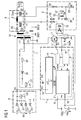
- FIG. 1 shows an electrical equivalent circuit diagram of a switching converter in which, in addition to a drive circuit 1 for a switch T connected in series with an inductive storage element L1, further circuit components of the switching converter are shown.
- Such a switching converter is used to generate a regulated output voltage Vout at output terminals of the switching converter from an input voltage Vin applied to input terminals.
- This input voltage Vin is a DC voltage, for example, by an input filter 6 with a Bridge rectifier D1-D4 and an input capacitor Cin, for example, from an AC voltage Vin 'may be generated.
- the illustrated switching converter is designed as a flyback converter and has a transformer TR with a primary winding and a secondary winding, whose primary winding L1 is connected in series with the switch T.
- the input voltage Vin is present across this series connection with the primary winding L1 and the switch T, which is connected between a terminal for the input voltage or the input potential Vin and a terminal for a primary-side reference potential GND1.
- the switch T of the switching converter shown in Figure 1 is realized as a MOS transistor, especially as an n-channel MOSFET, and driven by a generated by the drive circuit 1 drive signal S2.
- the drive signal S2 is in this case fed to a gate terminal of the MOSFET T.
- any other semiconductor switching elements in particular p-MOSFET or IGBT, can be used as a switch instead of the illustrated n-MOSFET.
- the transformer TR has a secondary winding L2, to which a rectifier circuit 8 is connected, which provides the output voltage Vout at the output terminals. Due to the operation of the switching converter, a pulse-shaped voltage is available at the secondary winding L2, which is converted by the rectifier circuit into a uniform output voltage Vout.
- the rectifier circuit shown in the example comprises a first rectifier with a diode D8 and a capacitor C8 and a second rectifier connected downstream of the first rectifier.
- the second rectifier comprises an inductance L8 and a capacitor Cout, wherein the capacitor Cout of the LC element forms an output capacitor of the switching converter. It should be noted that the two-stage rectifier arrangement 8 illustrated in FIG is to be considered only as an example and that any, the aforementioned rectifier function satisfying rectifier circuits can be used.
- the illustrated switching converter When the switch T is turned on, the illustrated switching converter absorbs energy via the input terminals, which is intermediately stored in the primary winding L1. In the case of switch T, which is subsequently blocked, this energy previously stored in primary winding L1 is transmitted to secondary winding L2 and via rectifier circuit 8 to the output terminals.
- the control signal S3 activating the switch T is a pulse-width-modulated signal whose duty cycle (duty cycle) determines the power consumption of the switching converter during a normal operating state to be explained.
- a control signal Vreg To regulate the power consumption, which takes place with the aim of keeping the output voltage Vout constant at least approximately independently of the input voltage Vin and at least approximately independently of the power consumption of a load Z connectable to the output terminals, a control signal Vreg is available ,
- This control signal Vreg is generated by a control signal generation circuit depending on the output voltage Vout, and is supplied to the drive circuit 1 via a control signal input 13.
- the control signal Vreg is available in the illustrated example via a capacitor Creg. This capacitor causes an integrating control behavior.
- the capacitor Creg can be connected to a terminal for a supply potential Vdd in the drive circuit-for example, via a resistor. This supply potential predetermines an initial value of the control signal, which is varied in the further course of the regulation as a function of the output voltage.
- the illustrated control signal generation circuit 9 is configured to compare the output voltage Vout with a reference value and to generate or modify the control signal Vreg so that the control signal becomes smaller with increasing difference between the output voltage Vout and the reference value when the output voltage Vout is greater than is the reference value, and that the control signal Vreg becomes larger with increasing difference between the reference value and the output voltage Vout when the output voltage Vout is smaller than the reference value.
- the control circuit 9 is arranged on the secondary side in the switching converter shown in Figure 1, the transmission of a control signal generated by this control circuit 9 to the primary side arranged drive circuit 1 via an optocoupler 10, which is connected to the primary side of the control capacitor Creg, via which a voltage available stands, which forms the feedback control signal Vreg.
- the control circuit 9 has a voltage divider 94, 98 connected to the output with a center tap, to which a measuring signal dependent on the output voltage Vout is available.
- the center tap is connected to a comparison and driver circuit 99, which compares the measurement signal with a reference value, which corresponds for example to the blocking voltage of a Zener diode, and which is connected to the optocoupler.
- a voltage supply of the control circuit 9 and the optocoupler 10 takes place in the example via the capacitor C8 of the rectifier arrangement 8, to which the optocoupler is connected via a resistor 92 and the comparison and driver circuit 99 via a resistor 93.
- a filter 95, 96, 97 which is connected between the resistor 93 and the center tap of the voltage divider, serves to regulate the output voltage.
- the drive circuit 1 has a drive signal generating circuit 2 which generates the drive signal S2 for the switch T in response to the control signal Vreg and a current measurement signal Vcs.
- a driver circuit 3 is connected which serves to convert a signal level of the drive signal provided by the drive signal generation circuit 2 to suitable signal levels for driving the switch T.
- a protection circuit 5 which serves, for example, to switch off the switching converter upon detection of a fault condition by interrupting a drive circuit of the switch T via the drive signal generation circuit 2 or the driver 3.
- the detection of an error can be done for example via the control signal Vreg or the current measurement signal Vcs.
- the drive circuit 1 also has an internal power supply circuit which serves to ensure a voltage supply of the circuit components present in the drive circuit 1.
- This internal power supply circuit 4 is connected to the input voltage Vin via a first terminal 15 and to an external power supply circuit 7 via a second terminal 16.
- the external power supply circuit 7 comprises an auxiliary winding L3 inductively coupled to the primary winding L1 and the secondary winding L2, and a rectifier arrangement coupled to this auxiliary winding L3, having a series arrangement of a diode D7 and a capacitor C7.
- a resistor R7 is also connected in series with these components.
- a supply voltage Vcc is available at this external power supply circuit 7 via the capacitor C7.
- the internal power supply circuit 4 is coupled to the input terminals, whereby an initial power supply is ensured. Due to a usually high voltage difference between the input voltage Vin and the supply voltage required for the voltage supply of the drive circuit 1, the provision of this supply voltage from the input voltage Vin is associated with high losses, so that the voltage supply via the input voltage Vin takes place only during a start-up phase of the switching converter.
- the internal power supply circuit 4 is configured accordingly and can be realized in a basically known manner.
- a switch 41 can be provided in the voltage supply circuit 4, which connects the terminal for the supply voltage Vcc to the terminal for the input voltage Vin as a function of a voltage across the capacitor C7. This switch is closed, for example, when the voltage across the capacitor C7 is below a predetermined threshold value to then charge the capacitor C7 via the input voltage Vin.
- the drive signal generation circuit 2 can assume two different operating states, a normal operating state and a so-called burst operating state, which are explained below with reference to FIGS. 2A and 2B.
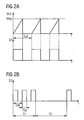
- FIG. 2A illustrates the generation of the drive signal S2 as a function of a current measurement signal Vcs' and the control signal Vreg during the normal operating state.
- the current measurement signal Vcs' shown here depends on the measuring voltage Vcs applied across the measuring resistor (Rcs in FIG. 1) and may be proportional to this measuring voltage Vcs, so that the following applies: Vcs' ⁇ cs
- the current measurement signal can also be proportional to an offset-biased measurement voltage, so that the following applies: Vcs' ⁇ cs + V offset where V offset denotes an offset value.
- drive pulses of the drive signal S2 are generated in time with a clock signal.
- a period of this clock signal is denoted by Tclk in FIG. 2a.
- the duration of the individual drive pulses is dependent on the control signal Vreg and the current measurement signal Vcs.
- the switching converter shown in Figure 1 is designed as a so-called current-mode switching converter. In the case of a conductive activation of the switch T, the current through the switch T, and therefore a voltage drop Vcs, rises linearly across a current measuring resistor Rcs connected in series with the switch T. The switch T remains closed until the current measurement signal Vcs reaches the value of the control signal Vreg or the value of a signal proportional to the control signal Vreg.
- the power consumption of the switching converter is the greater, the longer the individual drive pulses. If the output voltage Vout drops as a result of a higher power consumption of a connected load, the output voltage first decreases, as a result of which the amplitude of the control signal Vreg increases and the duration of the drive pulses likewise increase in order to increase the power consumption and thereby counteract a further decrease in the output voltage Vout. If, on the other hand, the power consumption of the load Z decreases and, as a result, the output voltage Vout initially increases, the control signal decreases, as a result of which the drive pulses shorten in order to reduce the power consumption and to counteract a further increase in the output voltage Vout.
- the drive signal generating circuit 2 In the burst operating mode, the drive signal generating circuit 2 generates the drive signal S2 such that drive intervals and drive pauses alternate. While control intervals of the one shown in Figure 2B and designated T1, a clocked control of the switch T is carried out by each equal-length drive pulses that can be generated in time with a clock signal. A period Tclk of this clock signal during burst operation may correspond to a period of the clock signal during normal operation. Tbp in Fig. 2B denotes the pulse duration of a drive pulse during the burst operation mode. During a drive pause, which is denoted by T2 in FIG. 2B, a blocking actuation of the switch T takes place permanently via the drive signal S2.
- FIG. 3 exemplarily illustrates a time profile of the control signal Vreg and the respective operating state of the switching converter, N denoting the normal operating state and B the burst operating state.
- the control signal Vreg reaches or falls below the value of a first reference signal Vben at a time t1.
- a transition to the burst mode B occurs, which in the example starts with a drive pause.
- the output voltage Vout decreases, as a result of which the control signal Vreg rises.
- the control signal Vreg reaches, at a second time t2, a second reference value Vbon during which a switch-off pause is switched over to a drive interval within the burst operating state the switch T is driven clocked in the manner explained with reference to Figure 2B.
- the output voltage Vout increases during the An horrintervalls, d. H.
- the control signal Vreg decreases.
- the drive interval ends in the illustrated example at a time t3, at which the control signal Vreg has dropped to a third reference value Vboff.
- the switch remains locked, whereby the control signal Vreg rises again until it reaches the value of the second reference value Vbon again at a further time t4.
- the drive signal generating circuit 2 illustrated in FIG. 4 has a pulse width modulator 21 and an operating state circuit 22 which generates the operating state indicating first and second operating state signals ST1, ST2.
- These operating state signals of which a first operating state signal ST1 indicates whether the switching converter is in the normal operating state or in the burst operating state, and of which a second operating state signal ST2 indicates whether the switching converter is within the burst operating state in a drive interval or in a drive pause , be through the Operating state circuit 22 is generated depending on a comparison of the control signal Vreg with the reference signals Vbon, Vboff, Vben and Vbex.
- the first state signal ST1 is available in this circuit at the output of a first flip-flop 221, which is set by a first comparator 223 depending on a comparison of the first reference signal Vben with the control signal Vreg and by a second comparator 224 depending on a comparison of the fourth reference signal Vbex is reset with the control signal Vreg.
- An output of the first comparator 223 is in this case connected to the set input S of the first flip-flop 221 and an output of the second comparator 224 is connected to a reset input R of this flip-flop 221.
- the first flip-flop 221 is set in the illustrated example when the control signal Vreg falls below the first reference value Vben and is reset when the control signal Vreg rises above the value of the fourth reference signal Vbex.
- the first state signal ST1 is a two-valued signal which assumes a high level during burst operation and a low level during normal operation.
- the second state signal ST2 is available at the output of a second flip-flop 222, which is set by a third comparator 225 depending on a comparison of the third reference signal Vbon with the control signal Vreg and by a fourth comparator 226 depending on a comparison of the third reference signal Vboff is reset with the control signal Vreg.
- An output of the third comparator 225 is here connected to the set input of the second flip-flop 222, and an output of the fourth comparator 226 is connected to the reset input of this second flip-flop 222.
- the flip-flop 222 is set when the control signal Vreg rises above the value of the second reference signal Vbon and is reset when the control signal Vreg falls below the value of the second reference signal Vboff.
- the second state signal ST2 in the example is a bivalent signal that is in burst mode during the drive intervals assumes a high level and assumes a low level in burst mode during the control pauses.
- the second and third reference signals Vbon, Vboff are generated in a manner not shown by a reference signal generating circuit (not shown).
- a further reference signal generating circuit 25 is provided, the structure and mode of operation of which will be explained below.
- the drive signal S2 is generated by the pulse width modulator 21 in a manner already explained with reference to FIGS. 2A and 2B, depending on the control signal Vreg, the current measurement signal Vcs and the two state signals ST1, ST2 which predetermine the respective operating state.
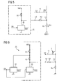
- This reference signal generating circuit 25 includes a voltage divider having voltage dividing resistors R1, R2 connected in series between a terminal for the supply potential Vdd of the drive signal generating circuit 2 and the primary-side reference potential GND 1.
- the voltage divider R1, R2 is connected in the illustrated example via the measuring input 12 and the current measuring resistor Rs to the primary-side reference potential GND1, so that the drive circuit (1 in Figure 1) requires no additional terminal for connecting this voltage divider to the primary-side reference potential GND1.
- the reference signal generating circuit 25 further includes a sample and hold circuit 26 connected between a center tap of the voltage divider and the primary-side reference potential GND1, that is, in the example, parallel to Series connection of the second voltage divider resistor R2 and the current measuring resistor Rs is connected.
- This sample and hold member 26 is for detecting a voltage applied across the series circuit of the second voltage dividing resistor R2 and the current measuring resistor Rs in accordance with an enable signal EN and for providing one of the first and fourth reference voltages Vben, Vbex.
- the reference symbol Vref in FIG. 5 stands for one of these two reference voltages.
- Vref R ⁇ 2 / R ⁇ 1 + R ⁇ 2 ⁇ Vdd
- the reference voltage Vref is thus proportional to the supply potential Vdd of the drive signal generating circuit 25 via the divider ratio of the voltage divider 25.
- This supply potential Vdd which is generated by the voltage supply circuit 4, can be regarded as approximately constant in the steady state of the switching converter.
- the reference voltage Vref is thus adjustable via the voltage divider R1, R2.
- the drive circuit (1 in FIG. 1) can be partially realized as an integrated circuit.
- the second voltage divider resistor R2 can be realized here as an external resistor which is connected to the integrated circuit via a connection terminal 12 '.
- the first resistor R1 can in this case together with other circuit components of Drive circuit 1 can be realized in the integrated circuit.
- the reference voltage Vref can be set exactly and simply via the second voltage divider resistor R2 in the knowledge of the resistance value of the integrated first voltage divider resistor R1 and in the knowledge of the supply voltage Vdd.
- the second voltage divider resistor R2 in this case functions as a setting resistor for the at least one reference value generated by the reference signal generating circuit 25.
- An adjustment of the reference value can be made as needed, for example, depending on the type of load to be supplied by the switching converter.
- the reference values in which a transition from normal operation to burst operation, or a transition from burst operation to normal operation, respectively represent different output powers of the switching converter.
- the output powers in which a change between the normal operation and the burst operation is carried out flexibly via the second voltage divider resistor R2.
- the enable signal EN is in the illustrated reference signal generating circuit 25 depends on the switching state of the switch T and is selected so that the sample and hold member is enabled only during such periods to sample the voltage across the voltage divider voltage during which the switch T blocks. This prevents the reference signal Vref from being superimposed by a signal component which depends on a current through the switch T.
- the voltage applied across the voltage divider R1, R2 is sampled in the burst mode, for example during drive pauses.
- the enable signal EN can, for example, this 4 correspond to the second state signal (ST2 in FIG. 4), wherein the sample and hold element 26 is realized when using an operating state circuit 22 shown in FIG. 4 such that the sample and hold element samples the voltage across the voltage divider at a low level of the enable signal ,
- the enable signal EN can also be derived directly from the drive signal S2 of the switch T, for example for generating the first reference value, which determines the transition from the normal operating state to the burst operating state.
- the reference voltage Vref available at the output of the sample and hold can be used as one of the two first and fourth reference voltages Vben, Vbex.
- An implementation example of a reference signal generation circuit 25 that generates both of the first and fourth reference voltages Vben, Vbex is shown in FIG.
- This reference signal generating circuit 25 comprises a voltage divider with three voltage divider resistors R1, R2, R3, which for example results from the voltage divider according to FIG. 5 by inserting an additional voltage divider resistor R3 between the first and second voltage divider resistors R1, R2.
- a first sample and hold member is connected in this circuit arrangement to a first voltage tap of the voltage divider between the second and third voltage divider resistor R2, R3 and provides at its output the fourth reference voltage Vboff available.
- the reference signal generating circuit 25 has a further sample and hold member which is connected to a second voltage tap of the voltage divider between the first and third voltage divider resistor R1, R3 and which provides at its output the first reference voltage Vben.
- the enable signal EN is derived in this arrangement, for example, directly from the drive signal S2 of the switch T.
- the sample and hold element 26 comprises a series connection of a switch 261 and a capacitor 262, which are connected between the voltage input of the sample and hold element 26 and the primary-side reference potential GND1.
- the switch 261 is driven by the enable signal EN and is at a predetermined signal level, that is, the signal level at which the enable signal EN releases the the triggering holding member 26, conductively energized, thereby charging the capacitor 262 to the voltage applied to the voltage input.
- the voltage applied across the capacitor 262 corresponds to the reference voltage Vref.
- the switch 261 in FIG. 7 can be replaced by a voltage follower controlled by the enable signal EN.
- FIG. 1 Another realization example of a sample and hold element is shown in FIG.
- This sample and hold circuit generates two reference voltages from the reference voltage Vref applied across the capacitor 262 by connecting the capacitor 262 to an analog-to-digital converter 264 which provides a digital value corresponding to the voltage across the capacitor 262.
- a processing unit 265 connected downstream of the analog-to-digital converter 264 generates the two reference voltages Vben, Vbex from this digital value.
- the second and third reference voltages Vbon, Vboff may also be generated as required by one of the reference signal generating circuits explained above.
- This pulse width modulation circuit 21 comprises two pulse width modulators 23, 24, to each of which a clock signal CLK of a clock generator 211 is supplied.
- a first pulse width modulator 23 generates a first pulse width modulated signal S23 depending on the clock signal CLK, the control signal Vreg and the current measurement signal Vcs which is supplied to a multiplexer 218.
- a second pulse width modulator 24 generates a second pulse width modulated signal 24 as a function of the clock signal CLK and the second state signal ST2, which is also supplied to the multiplexer 218.
- the multiplexer 218 is driven by the first state signal ST1 and during normal operation, the first pulse width modulated signal S23 as the control signal S2 and during the burst operation, the second pulse width modulated signal S24 as the drive signal S2 on.
- the first pulse width modulator 23 comprises a flip-flop 212 whose set input S is supplied with the clock signal CLK and which is thus set in time with this clock signal S. To a reset input R of this flip-flop 212, an output of a comparator 214 is connected to which the current measurement signal Vcs and the control signal Vreg are supplied and the flip-flop 212 resets each case when the current measurement signal Vcs' up to the value of the control signal Vreg has risen.
- the second pulse width modulator 24 comprises a further flip-flop 213 whose set input S is supplied with the clock signal CLK in accordance with the second state signal ST2 via a switch 217.
- This switch 217 is closed under control of the second state signal ST2 during drive intervals to set the flip-flop 213 clocked by the clock signal CLK.
- the signal supplied to the set input S of the flip-flop 213 is supplied to the reset input R of the flip-flop 213 with a time delay via a delay element 216 to the flip-flop 213 each reset a predetermined period corresponding to the desired pulse duration during the burst operation (Tbp in Figure 2B).
- the reset input R of this flip-flop 213 is preceded by an OR gate 215 to which the output signal of the delay element 216 and the second state signal ST2 are supplied.
- This OR gate 215 ensures that the flip-flop 213 is safely reset during burst operation upon a change from a drive interval to a drive break.
- the second operating state signal which changes to a low level during a transition from a drive interval to a drive pause, is supplied to the OR gate in this case via an inverting input.
Landscapes
- Engineering & Computer Science (AREA)
- Power Engineering (AREA)
- Dc-Dc Converters (AREA)
Priority Applications (2)
| Application Number | Priority Date | Filing Date | Title |
|---|---|---|---|
| DE200650003628 DE502006003628D1 (de) | 2006-10-31 | 2006-10-31 | Ansteuerschaltung für einen Schalter in einem Schaltwandler mit Burst-Betriebsmodus |
| EP20060022720 EP1919067B1 (fr) | 2006-10-31 | 2006-10-31 | Circuit de contrôle pour un commutateur dans une alimentation à découpage avec mode rafale |
Applications Claiming Priority (1)
| Application Number | Priority Date | Filing Date | Title |
|---|---|---|---|
| EP20060022720 EP1919067B1 (fr) | 2006-10-31 | 2006-10-31 | Circuit de contrôle pour un commutateur dans une alimentation à découpage avec mode rafale |
Publications (2)
| Publication Number | Publication Date |
|---|---|
| EP1919067A1 true EP1919067A1 (fr) | 2008-05-07 |
| EP1919067B1 EP1919067B1 (fr) | 2009-04-29 |
Family
ID=37890177
Family Applications (1)
| Application Number | Title | Priority Date | Filing Date |
|---|---|---|---|
| EP20060022720 Ceased EP1919067B1 (fr) | 2006-10-31 | 2006-10-31 | Circuit de contrôle pour un commutateur dans une alimentation à découpage avec mode rafale |
Country Status (2)
| Country | Link |
|---|---|
| EP (1) | EP1919067B1 (fr) |
| DE (1) | DE502006003628D1 (fr) |
Cited By (2)
| Publication number | Priority date | Publication date | Assignee | Title |
|---|---|---|---|---|
| CN103326584A (zh) * | 2012-03-20 | 2013-09-25 | 英飞凌科技奥地利有限公司 | 在待机模式下具有降低的功耗的功率转换器 |
| CN110289769A (zh) * | 2019-07-29 | 2019-09-27 | 惠州汇能精电科技有限公司 | 控制系统及供电系统 |
Citations (8)
| Publication number | Priority date | Publication date | Assignee | Title |
|---|---|---|---|---|
| US4937738A (en) * | 1984-08-31 | 1990-06-26 | Hitachi, Ltd. | Data processing system which selectively bypasses a cache memory in fetching information based upon bit information of an instruction |
| US5703764A (en) * | 1995-05-23 | 1997-12-30 | Deutsche Thomson Brandt Gmbh | Switched-mode power supply having standby operation |
| US6166926A (en) * | 2000-01-11 | 2000-12-26 | Thomson Licensing S.A. | Zero voltage switching power supply with burst mode |
| DE10146549A1 (de) * | 2001-09-21 | 2003-04-24 | Metz Werke Gmbh & Co Kg | Verfahren zum Betrieb eines Schaltnetzteils sowie danach arbeitendes Schaltnetzteil |
| US20030117813A1 (en) * | 2001-12-21 | 2003-06-26 | Fairchild Korea Semiconductor, Ltd | Switching mode power supply |
| DE10205706A1 (de) * | 2002-02-12 | 2003-08-28 | Infineon Technologies Ag | Ansteuerschaltung für einen Schalter in einem Schaltnetzteil |
| WO2004030194A1 (fr) * | 2002-09-30 | 2004-04-08 | Infineon Technologies Ag | Blocs d'alimentation a mode de commutation |
| US20040120171A1 (en) * | 2002-12-18 | 2004-06-24 | Jin-Ho Choi | Control for a switching power supply having automatic burst mode operation |
-
2006
- 2006-10-31 DE DE200650003628 patent/DE502006003628D1/de active Active
- 2006-10-31 EP EP20060022720 patent/EP1919067B1/fr not_active Ceased
Patent Citations (8)
| Publication number | Priority date | Publication date | Assignee | Title |
|---|---|---|---|---|
| US4937738A (en) * | 1984-08-31 | 1990-06-26 | Hitachi, Ltd. | Data processing system which selectively bypasses a cache memory in fetching information based upon bit information of an instruction |
| US5703764A (en) * | 1995-05-23 | 1997-12-30 | Deutsche Thomson Brandt Gmbh | Switched-mode power supply having standby operation |
| US6166926A (en) * | 2000-01-11 | 2000-12-26 | Thomson Licensing S.A. | Zero voltage switching power supply with burst mode |
| DE10146549A1 (de) * | 2001-09-21 | 2003-04-24 | Metz Werke Gmbh & Co Kg | Verfahren zum Betrieb eines Schaltnetzteils sowie danach arbeitendes Schaltnetzteil |
| US20030117813A1 (en) * | 2001-12-21 | 2003-06-26 | Fairchild Korea Semiconductor, Ltd | Switching mode power supply |
| DE10205706A1 (de) * | 2002-02-12 | 2003-08-28 | Infineon Technologies Ag | Ansteuerschaltung für einen Schalter in einem Schaltnetzteil |
| WO2004030194A1 (fr) * | 2002-09-30 | 2004-04-08 | Infineon Technologies Ag | Blocs d'alimentation a mode de commutation |
| US20040120171A1 (en) * | 2002-12-18 | 2004-06-24 | Jin-Ho Choi | Control for a switching power supply having automatic burst mode operation |
Cited By (3)
| Publication number | Priority date | Publication date | Assignee | Title |
|---|---|---|---|---|
| CN103326584A (zh) * | 2012-03-20 | 2013-09-25 | 英飞凌科技奥地利有限公司 | 在待机模式下具有降低的功耗的功率转换器 |
| US9602018B2 (en) | 2012-03-20 | 2017-03-21 | Infineon Technologies Austria Ag | Power converter with reduced power consumption in standby mode |
| CN110289769A (zh) * | 2019-07-29 | 2019-09-27 | 惠州汇能精电科技有限公司 | 控制系统及供电系统 |
Also Published As
| Publication number | Publication date |
|---|---|
| EP1919067B1 (fr) | 2009-04-29 |
| DE502006003628D1 (de) | 2009-06-10 |
Similar Documents
| Publication | Publication Date | Title |
|---|---|---|
| DE10040413B4 (de) | Schaltungsanordnung zur Erzeugung eines Schaltsignals für ein stromgesteuertes Schaltnetzteil | |
| DE69603697T2 (de) | Schaltnetzteil mit transformator und rückkopplung durch primärwicklung | |
| DE102009045052B4 (de) | Bereitstellen einer Versorgungsspannung für eine Ansteuerschaltung eines Halbleiterschaltelements | |
| DE102009001531A1 (de) | Gleichrichterschaltung | |
| EP0526693A2 (fr) | Circuit de démarrage pour un bloc d'alimentation à commutation | |
| EP2110938B1 (fr) | Circuit de commande primaire pour un convertisseur électronique de puissance comportant un transformateur sans enroulement auxiliaire avec un réglage basé sur la durée de continuité de courant du côté secondaire | |
| EP0205630A1 (fr) | Régulateur de découpage et son application | |
| WO1995020261A1 (fr) | Convertisseur de blocage a tension de sortie regulee | |
| DE3026147C2 (de) | Geregelter fremdgetakteter Gleichspannungswandler | |
| EP1919067B1 (fr) | Circuit de contrôle pour un commutateur dans une alimentation à découpage avec mode rafale | |
| DE19918041B4 (de) | Schaltnetzteil und Verfahren zur Ansteuerung eines Schalters in einem Schaltnetzteil | |
| DE2608167B2 (de) | Geregelter Eintakt-Durchflußumrichter zur Erzeugung mehrerer galvanisch getrennter Ausgangsspannungen | |
| DE10325519A1 (de) | Ansteuerschaltung für einen Schalter in einem Schaltwandler | |
| DE10339470A1 (de) | Steuerschaltung für ein Schaltnetzteil | |
| EP0509343B1 (fr) | Méthode de fonctionnement d'un régulateur à découpage et son dispositif | |
| DE3134599C2 (de) | Verfahren und Schaltungsanordnung zur Regelung der Ausgangsspannung eines fremdgesteuerten Gleichspannungswandlers | |
| EP0301386A2 (fr) | Alimentation régulée à découpage | |
| DE3300285C2 (de) | Elektronisches Schaltnetzteil | |
| EP1533903B1 (fr) | Procédé et dispositif pour la transmission des commutations avec isolation galvanique | |
| AT500563B1 (de) | Schaltwandler | |
| DE3110075C2 (de) | Strombegrenzer für einen Sperrumrichter | |
| EP0913025B1 (fr) | Bloc d'alimentation a decoupage | |
| DE19730220A1 (de) | Getaktete Stromversorgungsanordnung | |
| DE3246320C2 (de) | Gleichspannungswandler | |
| DE10205706B4 (de) | Ansteuerschaltung für einen Schalter in einem Schaltnetzteil |
Legal Events
| Date | Code | Title | Description |
|---|---|---|---|
| PUAI | Public reference made under article 153(3) epc to a published international application that has entered the european phase |
Free format text: ORIGINAL CODE: 0009012 |
|
| 17P | Request for examination filed |
Effective date: 20070512 |
|
| AK | Designated contracting states |
Kind code of ref document: A1 Designated state(s): AT BE BG CH CY CZ DE DK EE ES FI FR GB GR HU IE IS IT LI LT LU LV MC NL PL PT RO SE SI SK TR |
|
| AX | Request for extension of the european patent |
Extension state: AL BA HR MK RS |
|
| GRAP | Despatch of communication of intention to grant a patent |
Free format text: ORIGINAL CODE: EPIDOSNIGR1 |
|
| AKX | Designation fees paid |
Designated state(s): DE FR GB IT |
|
| GRAS | Grant fee paid |
Free format text: ORIGINAL CODE: EPIDOSNIGR3 |
|
| GRAA | (expected) grant |
Free format text: ORIGINAL CODE: 0009210 |
|
| AK | Designated contracting states |
Kind code of ref document: B1 Designated state(s): DE FR GB IT |
|
| REG | Reference to a national code |
Ref country code: GB Ref legal event code: FG4D Free format text: NOT ENGLISH |
|
| REF | Corresponds to: |
Ref document number: 502006003628 Country of ref document: DE Date of ref document: 20090610 Kind code of ref document: P |
|
| PLBE | No opposition filed within time limit |
Free format text: ORIGINAL CODE: 0009261 |
|
| STAA | Information on the status of an ep patent application or granted ep patent |
Free format text: STATUS: NO OPPOSITION FILED WITHIN TIME LIMIT |
|
| 26N | No opposition filed |
Effective date: 20100201 |
|
| REG | Reference to a national code |
Ref country code: FR Ref legal event code: PLFP Year of fee payment: 10 |
|
| REG | Reference to a national code |
Ref country code: FR Ref legal event code: PLFP Year of fee payment: 11 |
|
| REG | Reference to a national code |
Ref country code: FR Ref legal event code: PLFP Year of fee payment: 12 |
|
| REG | Reference to a national code |
Ref country code: FR Ref legal event code: PLFP Year of fee payment: 13 |
|
| PGFP | Annual fee paid to national office [announced via postgrant information from national office to epo] |
Ref country code: GB Payment date: 20211022 Year of fee payment: 16 Ref country code: DE Payment date: 20211206 Year of fee payment: 16 |
|
| PGFP | Annual fee paid to national office [announced via postgrant information from national office to epo] |
Ref country code: IT Payment date: 20211028 Year of fee payment: 16 Ref country code: FR Payment date: 20211021 Year of fee payment: 16 |
|
| REG | Reference to a national code |
Ref country code: DE Ref legal event code: R119 Ref document number: 502006003628 Country of ref document: DE |
|
| GBPC | Gb: european patent ceased through non-payment of renewal fee |
Effective date: 20221031 |
|
| PG25 | Lapsed in a contracting state [announced via postgrant information from national office to epo] |
Ref country code: FR Free format text: LAPSE BECAUSE OF NON-PAYMENT OF DUE FEES Effective date: 20221031 Ref country code: DE Free format text: LAPSE BECAUSE OF NON-PAYMENT OF DUE FEES Effective date: 20230503 |
|
| PG25 | Lapsed in a contracting state [announced via postgrant information from national office to epo] |
Ref country code: IT Free format text: LAPSE BECAUSE OF NON-PAYMENT OF DUE FEES Effective date: 20221031 Ref country code: GB Free format text: LAPSE BECAUSE OF NON-PAYMENT OF DUE FEES Effective date: 20221031 |