EP1921597A2 - Antriebsverfahren für eine Anzeige - Google Patents
Antriebsverfahren für eine Anzeige Download PDFInfo
- Publication number
- EP1921597A2 EP1921597A2 EP07254353A EP07254353A EP1921597A2 EP 1921597 A2 EP1921597 A2 EP 1921597A2 EP 07254353 A EP07254353 A EP 07254353A EP 07254353 A EP07254353 A EP 07254353A EP 1921597 A2 EP1921597 A2 EP 1921597A2
- Authority
- EP
- European Patent Office
- Prior art keywords
- scan
- subframe
- display
- frame
- subframes
- Prior art date
- Legal status (The legal status is an assumption and is not a legal conclusion. Google has not performed a legal analysis and makes no representation as to the accuracy of the status listed.)
- Withdrawn
Links
Images


Classifications
-
- G—PHYSICS
- G09—EDUCATION; CRYPTOGRAPHY; DISPLAY; ADVERTISING; SEALS
- G09G—ARRANGEMENTS OR CIRCUITS FOR CONTROL OF INDICATING DEVICES USING STATIC MEANS TO PRESENT VARIABLE INFORMATION
- G09G3/00—Control arrangements or circuits, of interest only in connection with visual indicators other than cathode-ray tubes
- G09G3/20—Control arrangements or circuits, of interest only in connection with visual indicators other than cathode-ray tubes for presentation of an assembly of a number of characters, e.g. a page, by composing the assembly by combination of individual elements arranged in a matrix no fixed position being assigned to or needed to be assigned to the individual characters or partial characters
- G09G3/22—Control arrangements or circuits, of interest only in connection with visual indicators other than cathode-ray tubes for presentation of an assembly of a number of characters, e.g. a page, by composing the assembly by combination of individual elements arranged in a matrix no fixed position being assigned to or needed to be assigned to the individual characters or partial characters using controlled light sources
- G09G3/30—Control arrangements or circuits, of interest only in connection with visual indicators other than cathode-ray tubes for presentation of an assembly of a number of characters, e.g. a page, by composing the assembly by combination of individual elements arranged in a matrix no fixed position being assigned to or needed to be assigned to the individual characters or partial characters using controlled light sources using electroluminescent panels
-
- G—PHYSICS
- G09—EDUCATION; CRYPTOGRAPHY; DISPLAY; ADVERTISING; SEALS
- G09G—ARRANGEMENTS OR CIRCUITS FOR CONTROL OF INDICATING DEVICES USING STATIC MEANS TO PRESENT VARIABLE INFORMATION
- G09G3/00—Control arrangements or circuits, of interest only in connection with visual indicators other than cathode-ray tubes
- G09G3/20—Control arrangements or circuits, of interest only in connection with visual indicators other than cathode-ray tubes for presentation of an assembly of a number of characters, e.g. a page, by composing the assembly by combination of individual elements arranged in a matrix no fixed position being assigned to or needed to be assigned to the individual characters or partial characters
- G09G3/2007—Display of intermediate tones
- G09G3/2018—Display of intermediate tones by time modulation using two or more time intervals
- G09G3/2022—Display of intermediate tones by time modulation using two or more time intervals using sub-frames
-
- G—PHYSICS
- G09—EDUCATION; CRYPTOGRAPHY; DISPLAY; ADVERTISING; SEALS
- G09G—ARRANGEMENTS OR CIRCUITS FOR CONTROL OF INDICATING DEVICES USING STATIC MEANS TO PRESENT VARIABLE INFORMATION
- G09G3/00—Control arrangements or circuits, of interest only in connection with visual indicators other than cathode-ray tubes
- G09G3/20—Control arrangements or circuits, of interest only in connection with visual indicators other than cathode-ray tubes for presentation of an assembly of a number of characters, e.g. a page, by composing the assembly by combination of individual elements arranged in a matrix no fixed position being assigned to or needed to be assigned to the individual characters or partial characters
-
- G—PHYSICS
- G09—EDUCATION; CRYPTOGRAPHY; DISPLAY; ADVERTISING; SEALS
- G09G—ARRANGEMENTS OR CIRCUITS FOR CONTROL OF INDICATING DEVICES USING STATIC MEANS TO PRESENT VARIABLE INFORMATION
- G09G3/00—Control arrangements or circuits, of interest only in connection with visual indicators other than cathode-ray tubes
- G09G3/20—Control arrangements or circuits, of interest only in connection with visual indicators other than cathode-ray tubes for presentation of an assembly of a number of characters, e.g. a page, by composing the assembly by combination of individual elements arranged in a matrix no fixed position being assigned to or needed to be assigned to the individual characters or partial characters
- G09G3/2007—Display of intermediate tones
- G09G3/2018—Display of intermediate tones by time modulation using two or more time intervals
- G09G3/2022—Display of intermediate tones by time modulation using two or more time intervals using sub-frames
- G09G3/2033—Display of intermediate tones by time modulation using two or more time intervals using sub-frames with splitting one or more sub-frames corresponding to the most significant bits into two or more sub-frames
-
- G—PHYSICS
- G09—EDUCATION; CRYPTOGRAPHY; DISPLAY; ADVERTISING; SEALS
- G09G—ARRANGEMENTS OR CIRCUITS FOR CONTROL OF INDICATING DEVICES USING STATIC MEANS TO PRESENT VARIABLE INFORMATION
- G09G3/00—Control arrangements or circuits, of interest only in connection with visual indicators other than cathode-ray tubes
- G09G3/20—Control arrangements or circuits, of interest only in connection with visual indicators other than cathode-ray tubes for presentation of an assembly of a number of characters, e.g. a page, by composing the assembly by combination of individual elements arranged in a matrix no fixed position being assigned to or needed to be assigned to the individual characters or partial characters
- G09G3/22—Control arrangements or circuits, of interest only in connection with visual indicators other than cathode-ray tubes for presentation of an assembly of a number of characters, e.g. a page, by composing the assembly by combination of individual elements arranged in a matrix no fixed position being assigned to or needed to be assigned to the individual characters or partial characters using controlled light sources
- G09G3/30—Control arrangements or circuits, of interest only in connection with visual indicators other than cathode-ray tubes for presentation of an assembly of a number of characters, e.g. a page, by composing the assembly by combination of individual elements arranged in a matrix no fixed position being assigned to or needed to be assigned to the individual characters or partial characters using controlled light sources using electroluminescent panels
- G09G3/32—Control arrangements or circuits, of interest only in connection with visual indicators other than cathode-ray tubes for presentation of an assembly of a number of characters, e.g. a page, by composing the assembly by combination of individual elements arranged in a matrix no fixed position being assigned to or needed to be assigned to the individual characters or partial characters using controlled light sources using electroluminescent panels semiconductive, e.g. using light-emitting diodes [LED]
-
- H—ELECTRICITY
- H05—ELECTRIC TECHNIQUES NOT OTHERWISE PROVIDED FOR
- H05B—ELECTRIC HEATING; ELECTRIC LIGHT SOURCES NOT OTHERWISE PROVIDED FOR; CIRCUIT ARRANGEMENTS FOR ELECTRIC LIGHT SOURCES, IN GENERAL
- H05B33/00—Electroluminescent light sources
-
- G—PHYSICS
- G09—EDUCATION; CRYPTOGRAPHY; DISPLAY; ADVERTISING; SEALS
- G09G—ARRANGEMENTS OR CIRCUITS FOR CONTROL OF INDICATING DEVICES USING STATIC MEANS TO PRESENT VARIABLE INFORMATION
- G09G2310/00—Command of the display device
- G09G2310/02—Addressing, scanning or driving the display screen or processing steps related thereto
- G09G2310/0224—Details of interlacing
-
- G—PHYSICS
- G09—EDUCATION; CRYPTOGRAPHY; DISPLAY; ADVERTISING; SEALS
- G09G—ARRANGEMENTS OR CIRCUITS FOR CONTROL OF INDICATING DEVICES USING STATIC MEANS TO PRESENT VARIABLE INFORMATION
- G09G2320/00—Control of display operating conditions
- G09G2320/02—Improving the quality of display appearance
- G09G2320/0247—Flicker reduction other than flicker reduction circuits used for single beam cathode-ray tubes
-
- G—PHYSICS
- G09—EDUCATION; CRYPTOGRAPHY; DISPLAY; ADVERTISING; SEALS
- G09G—ARRANGEMENTS OR CIRCUITS FOR CONTROL OF INDICATING DEVICES USING STATIC MEANS TO PRESENT VARIABLE INFORMATION
- G09G2320/00—Control of display operating conditions
- G09G2320/02—Improving the quality of display appearance
- G09G2320/0261—Improving the quality of display appearance in the context of movement of objects on the screen or movement of the observer relative to the screen
-
- G—PHYSICS
- G09—EDUCATION; CRYPTOGRAPHY; DISPLAY; ADVERTISING; SEALS
- G09G—ARRANGEMENTS OR CIRCUITS FOR CONTROL OF INDICATING DEVICES USING STATIC MEANS TO PRESENT VARIABLE INFORMATION
- G09G2320/00—Control of display operating conditions
- G09G2320/02—Improving the quality of display appearance
- G09G2320/0266—Reduction of sub-frame artefacts
-
- G—PHYSICS
- G09—EDUCATION; CRYPTOGRAPHY; DISPLAY; ADVERTISING; SEALS
- G09G—ARRANGEMENTS OR CIRCUITS FOR CONTROL OF INDICATING DEVICES USING STATIC MEANS TO PRESENT VARIABLE INFORMATION
- G09G3/00—Control arrangements or circuits, of interest only in connection with visual indicators other than cathode-ray tubes
- G09G3/20—Control arrangements or circuits, of interest only in connection with visual indicators other than cathode-ray tubes for presentation of an assembly of a number of characters, e.g. a page, by composing the assembly by combination of individual elements arranged in a matrix no fixed position being assigned to or needed to be assigned to the individual characters or partial characters
- G09G3/22—Control arrangements or circuits, of interest only in connection with visual indicators other than cathode-ray tubes for presentation of an assembly of a number of characters, e.g. a page, by composing the assembly by combination of individual elements arranged in a matrix no fixed position being assigned to or needed to be assigned to the individual characters or partial characters using controlled light sources
- G09G3/30—Control arrangements or circuits, of interest only in connection with visual indicators other than cathode-ray tubes for presentation of an assembly of a number of characters, e.g. a page, by composing the assembly by combination of individual elements arranged in a matrix no fixed position being assigned to or needed to be assigned to the individual characters or partial characters using controlled light sources using electroluminescent panels
- G09G3/32—Control arrangements or circuits, of interest only in connection with visual indicators other than cathode-ray tubes for presentation of an assembly of a number of characters, e.g. a page, by composing the assembly by combination of individual elements arranged in a matrix no fixed position being assigned to or needed to be assigned to the individual characters or partial characters using controlled light sources using electroluminescent panels semiconductive, e.g. using light-emitting diodes [LED]
- G09G3/3208—Control arrangements or circuits, of interest only in connection with visual indicators other than cathode-ray tubes for presentation of an assembly of a number of characters, e.g. a page, by composing the assembly by combination of individual elements arranged in a matrix no fixed position being assigned to or needed to be assigned to the individual characters or partial characters using controlled light sources using electroluminescent panels semiconductive, e.g. using light-emitting diodes [LED] organic, e.g. using organic light-emitting diodes [OLED]
- G09G3/3225—Control arrangements or circuits, of interest only in connection with visual indicators other than cathode-ray tubes for presentation of an assembly of a number of characters, e.g. a page, by composing the assembly by combination of individual elements arranged in a matrix no fixed position being assigned to or needed to be assigned to the individual characters or partial characters using controlled light sources using electroluminescent panels semiconductive, e.g. using light-emitting diodes [LED] organic, e.g. using organic light-emitting diodes [OLED] using an active matrix
- G09G3/3233—Control arrangements or circuits, of interest only in connection with visual indicators other than cathode-ray tubes for presentation of an assembly of a number of characters, e.g. a page, by composing the assembly by combination of individual elements arranged in a matrix no fixed position being assigned to or needed to be assigned to the individual characters or partial characters using controlled light sources using electroluminescent panels semiconductive, e.g. using light-emitting diodes [LED] organic, e.g. using organic light-emitting diodes [OLED] using an active matrix with pixel circuitry controlling the current through the light-emitting element
Definitions
- Embodiments of the present invention relate to a driving method of a display. More particularly, embodiments relate to a method for digitally driving a display.
- Flat panel displays include liquid crystal displays (LCDs), field emission displays (FEDs), plasma display panels (PDPs), and organic light emitting displays.
- LCDs liquid crystal displays
- FEDs field emission displays
- PDPs plasma display panels
- organic light emitting displays include organic light emitting displays.
- Organic light emitting displays make use of organic light emitting diodes (OLEDs) that emit light by re-combination of electrons and holes.
- OLEDs organic light emitting diodes
- An organic light emitting display has advantages of high response speed and small power consumption.
- a pixel of a conventional organic light emitting display may include an OLED and a pixel circuit, coupled to a data line Dm and a scan line Sn, to control the OLED, i.e., the OLED may generate light of a predetermined luminance corresponding to an electric current from the pixel circuit.
- the pixel circuit may control an amount of an electric current provided to the OLED corresponding to a data signal provided to the data line Dm.
- the pixel circuit may include a transistor and a storage capacitor.
- the transistor may be coupled between a first power supply and the OLED.
- the OLED may be between a second power supply and the pixel circuit.
- the transistor may control an amount of an electric current flowing from the first power supply ELVDD to the second power supply ELVSS through the OLED according to the voltage stored in the storage capacitor.
- exact expression of desired gradations may be difficult.
- the pixels should express a plurality of gradations using a constant voltage to be stored in the storage capacitor. Thus, in the conventional organic light emitting display, accurate brightness difference between adjacent gradations may not be expressed.
- the threshold voltage and electron mobility of the transistor may vary between pixels due to a process deviation.
- each pixel may generate light of different gradations in response to the same gradation voltage.
- the conventional organic light emitting display may not display an image of uniform luminance.
- Embodiments of the present invention are therefore directed to a method for driving a display, which substantially overcomes one or more of the problems due to the limitations and disadvantages of the related art.
- an organic light emitting display device having an interlace system for sequentially supplying a scan signal to odd numbered scan lines, followed by sequentially supplying a scan signal to even numbered scan lines to display one frame of a picture twice, wherein the organic light emitting display device is driven at a time difference of 1/2 frame period in a drive timing between the odd numbered scan lines and their adjacent even numbered scan lines.
- FIG. 1 illustrates an organic light emitting display according to an embodiment of the present invention
- FIG. 2 illustrates one frame in a method for driving an organic light emitting display according to an embodiment of the present invention
- FIG. 3 illustrates an occurrence of pseudo contour noise during a digital drive
- FIG. 4 illustrates one frame in a method for driving a display according to an embodiment of the present invention.
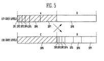
- FIG. 5 illustrates minimized pseudo contour noise using the driving method of FIG. 4 .
- FIG. 1 to FIG. 5 When one element is connected to another element one element may be not only directly connected to another element, but also may be indirectly connected to another element via another element. Further, irrelevant elements may be omitted for clarity. Also, like reference numerals refer to like elements throughout.
- FIG. 1 illustrates an organic light emitting display according to an embodiment of the present invention
- the organic light emitting display includes a pixel portion 30 having pixels 40, a scan driver 10, a data driver 20, and a timing control unit 50.
- the pixels 40 are connected to scan lines S1 through Sn and data lines D1 through Dm.
- the scan driver 10 drives the scan lines S 1 through Sn.
- the data driver 20 drives the data lines D1 through Dm.
- the timing control unit 50 controls the scan driver 10 and the data driver 20.
- the timing control unit 50 generates a data driving signal DCS and a scan driving signal SCS corresponding to externally supplied synchronizing signals.
- the data driving signal DCS generated from the timing control part 50 is provided to the data driver 20, and the scan driving signal SCS is provided to the scan driver 10. Further, the timing control unit 50 provides an externally supplied data DATA to the data driver 20.
- the scan driver 10 sequentially provides a scan signal to scan lines S1 to Sn every subframe period.
- the scan signal is sequentially provided to the scan lines S1 to Sn
- the pixels 40 are sequentially selected by lines, and the selected pixels 40 receive the first data signal or the second data signal from the data lines D1 to Dm.
- the pixel portion 30 receives power of the first power supply ELVDD and power of the second power supply ELVSS from the exterior, and supplies power to the pixels 40.
- the pixels 40 receive the power of the first power supply ELVDD and the power of the second power supply ELVSS
- the pixels 40 receive a data signal (the first data signal or the second data signal), and emit light or not according to the data signal.
- the pixels 40 that receive the first data signal emit light during a corresponding subframe period.
- the pixels 40 that receive the second data signal do not emit light during a corresponding subframe period.
- opposite logic may be used in accordance with a structure of the circuit controlling the pixels 40.
- FIG. 2 illustrates a method for driving one frame in an organic light emitting display according to an embodiment of the present invention.
- one frame 1F may be divided into a plurality of subframes SF1 ⁇ SF8 to be driven by digital drive.
- the respective subframes SF1 ⁇ SF8 may be divided into a scan period to sequentially supply a scan signal, an emission period to cause pixels 40 that receive the first data signal during the scan period to emit light, and a reset period to cause the pixels 40 to be changed into a non-emission state.
- the scan signal is sequentially provided to the scan lines S1 to Sn. Also during the scan period, the first data signal or the second data signal may be supplied to respective data lines D 1 to Dm. That is, the pixels 40 may receive the first data signal or the second data signal.
- the pixels 40 emit light or not during the emission period while maintaining the first data signal or the second data signal supplied during the scan period. That is, the pixels 40 that receive the first data signal during the scan period are set in an emission state during a corresponding subframe period, while the pixels 40 that receive the second data signal are set in a non-emission state during a corresponding subframe period.
- the one frame illustrated in FIG. 2 is merely one example of frames with which embodiments of the present invention may be employed. Thus, embodiments of the present invention are not limited thereto.
- one frame maybe divided into more than ten subframes, and an emission period of each subframe may be variously set by a designer.
- the pixels 40 are set to a non-emission state. Additional wirings and transistors may be further included in each of the pixels 40 to achieve this reset state. Alternatively, the reset period may be eliminated.
- the aforementioned digital drive expresses gradations using a turning-on or turning-off state of a transistor, an image of uniform luminance may be displayed. Furthermore, because embodiments of the invention express gradations using a time division, i.e., a digital drive, more exact gradations may be expressed as compared with expressing gradations using a constant voltage range, i.e., an analog drive.
- a region "A" expressing a gradation of 127 and a region “B” expressing a gradation of 128 adjacent thereto will appear to a viewer as a gradation of 255.
- a region “C” expressing a gradation of 128 and a region “D” expressing a gradation (grey level) of 127 adjacent thereto will appear as a gradation (grey level) of zero.
- Such pseudo contour noise is a main factor deteriorating display quality in a digital drive.
- a scan signal may be sequentially supplied to all the scan lines S 1 to Sn. Because the supply period of the scan signal to the scan lines S 1 to Sn does not contribute to emission, an emission time of the pixels 40 is shortened. In other words, when one frame includes eight subframes, a scan signal may be supplied to respective scan lines S 1 to Sn eight times, shortening emission time.
- the number of subframes may be increased to drive a display device, but the increase in the number of the subframes increases driving frequency.
- some embodiments of the present invention employ spatial averaging between adjacent lines, e.g., odd numbered scan lines and their adjacent even numbered scan lines.
- the adjacent lines are driven with a non-progressive scan system, e.g., an interlaced scan system, in which scan signals applied to adjacent lines may be offset by a fraction, e.g., 1 ⁇ 2, of a frame period.
- FIG. 4 illustrates one frame in a method for driving a display, e.g., an organic light emitting display, according to an embodiment of the present invention. While FIG. 4 illustrates one frame being divided into eight subframes, embodiments of the present invention are not limited thereto.
- a method for driving a display may reduce or eliminate flicker and/or false contour by a spatial averaging effect between adjacent lines by driving adjacent lines with signals having a time difference of a fraction, e.g., 1 ⁇ 2, of a frame period therebetween.
- offset signals may be supplied to odd numbered scan lines and adjacent even numbered scan lines in an interlace system, in which one frame of a picture is scanned twice, for example, by sequentially supplying a scan signal to the odd numbered scan lines and sequentially supplying a scan signal to the even numbered scan lines.
- Each of the subframes (SF1 ⁇ SF8) constituting one frame correspond to each bit of the data signal, wherein the least significant bit (LSB) corresponds to a first subframe (SF1), and the most significant bit (MSB) corresponds to an eighth subframe (SF8).
- LSB least significant bit
- MSB most significant bit
- a pixel may emit light during a corresponding subframe period when receiving a first data signal, e.g., "1”, and may not emit light when receiving a second data signal, e.g., "0".
- the pixels display a predetermined grey level of an image by controlling whether or not individual pixels 40 emit light in each of the subframes (SF1 ⁇ SF8).
- Each pixel 40 displays a predetermined grey level of an image during one frame period using the sum of the emission time of that pixel during the subframe periods.
- the one frame may be generally sequentially turned on in order of the first subframe (SF1) to the eighth subframe (SF8). Therefore, certain subframes are selected in order from the first subframe (SF1) to the eighth subframe (SF8) by the input digital data. Then, the selected subframes are allowed to emit light, and the grey levels are displayed in accordance with the sum of the emission time of the subframes.
- a pixel is to display a grey level of 127, i.e., input data is "01111111”, then the pixel emits light during the first subframe (SF1) to a seventh subframe (SF7), but not during the eighth subframe (SF8).
- a pixel is to display a grey level of 128, i.e., the input data is "10000000”, then the pixel does not emit light during the first subframe (SF1) to the seventh subframe (SF7), but does emit light during the eighth subframe (SF8).
- dynamic false contouring may be caused if a pixel displaying a grey level of 127 is adjacent to a pixel displaying a grey level of 128.
- embodiments of the present invention may reduce or eliminate flicker and/or false contour by a spatial averaging effect between adjacent lines being driven at a time difference of a fraction, e.g., 1 ⁇ 2, of a frame period in a drive timing between odd numbered scan lines and their adjacent even numbered scan lines in the interlace driving system.
- a spatial averaging effect between adjacent lines being driven at a time difference of a fraction, e.g., 1 ⁇ 2, of a frame period in a drive timing between odd numbered scan lines and their adjacent even numbered scan lines in the interlace driving system.
- one frame may be sequentially turned on in order of SF1, SF2, ..., SF8 for a first scan line (an odd numbered scan line), while being sequentially turned on in order of SF8, SF1, ..., SF7, e.g., may be shifted by 1 ⁇ 2 a frame period relative to the first scan line, for a second scan line (an even numbered scan line) adjacent to the first scan line.
- data of one frame may be displayed while being shifted at a predetermined time in subsequent odd numbered scan lines (3, 5, ..., 2 n -1), as shown in FIG. 4 .
- the predetermined time may correspond to an amount of time required to provide a signal to the final odd numbered 2 n -1 st scan line or at an interval of every x scan line identical to that of the first scan line.
- data of one frame may be displayed while being shifted at a predetermined time in subsequent even numbered scan lines (4, 6, ..., 2 n ), as shown in FIG. 4 , i.e., the time difference between subsequent adjacent odd and even scan lines may remain constant.
- a region of more significant bits may emit light in predetermined scan lines when less significant bits emit light in adjacent scan lines, while less significant bits may emit the light in predetermined scan lines when more significant bits emit the light in adjacent scan lines. This may reduce or eliminate dynamic false contour and/or flicker, since the spatially adjacent scan lines are averaged together.
- FIG. 5 illustrates how dynamic false contour may be reduced or eliminated in accordance with the driving method of FIG. 4 .
- FIG. 5 illustrates that the line of vision moves between a first pixel displaying a grey level of 127 (an odd numbered line) and a second pixel displaying a grey level of 128 (an even numbered line).
- Dynamic false contouring caused by a time difference in light emission of the MSB and less significant bits, may be compensated using the driving method.
- a first pixel of the odd numbered line is to display a grey level of 127, i.e., input data is "01111111”
- the first pixel emits light during the first subframe (SF1) to the seventh subframe (SF7), but not during the eighth subframe (SF8).
- a second pixel of the even numbered line, adjacent to the odd numbered line is to display a grey level of 128, i.e., input data is "10000000”
- the second pixel emits light during the eighth subframe (SF8), but not during the first subframe (SF1) to the seventh subframe (SF7).
- the region "B” will appear as a grey level of 0 when the region “A” displays a grey level of 127 and the region “B” displays a grey level of 0, as shown in FIG. 5 .
- the region “D” will appear as a grey level of 128 when the region “C” displays a grey level of 128 and the region “D” displays a grey level of 0.
- display quality may be maintained using the digital driving method illustrated in FIG. 4 even when displaying a quickly moving image.
- a display being driven in accordance with embodiments described above may reduce or eliminate flicker and/or false contour by a spatial averaging effect between adjacent lines being driven by signals offset from one another, e.g., by a difference of 1 ⁇ 2 a frame period.
- digital driving method of embodiments of the invention may reduce or eliminate false contour and/or flicker without an increase in the number of subframes, which may allow power consumption to be lowered, and may be implemented easily by changing a driving order, e.g., without installation of additional external parts.
Landscapes
- Engineering & Computer Science (AREA)
- Physics & Mathematics (AREA)
- Computer Hardware Design (AREA)
- General Physics & Mathematics (AREA)
- Theoretical Computer Science (AREA)
- Control Of El Displays (AREA)
- Control Of Indicators Other Than Cathode Ray Tubes (AREA)
- Electroluminescent Light Sources (AREA)
- Liquid Crystal Display Device Control (AREA)
Applications Claiming Priority (1)
| Application Number | Priority Date | Filing Date | Title |
|---|---|---|---|
| KR1020060110571A KR100844769B1 (ko) | 2006-11-09 | 2006-11-09 | 유기전계발광 표시장치의 구동방법 |
Publications (2)
| Publication Number | Publication Date |
|---|---|
| EP1921597A2 true EP1921597A2 (de) | 2008-05-14 |
| EP1921597A3 EP1921597A3 (de) | 2010-05-05 |
Family
ID=39020764
Family Applications (1)
| Application Number | Title | Priority Date | Filing Date |
|---|---|---|---|
| EP07254353A Withdrawn EP1921597A3 (de) | 2006-11-09 | 2007-11-02 | Antriebsverfahren für eine Anzeige |
Country Status (5)
| Country | Link |
|---|---|
| US (1) | US20080111837A1 (de) |
| EP (1) | EP1921597A3 (de) |
| JP (1) | JP2008122892A (de) |
| KR (1) | KR100844769B1 (de) |
| CN (1) | CN101178872A (de) |
Cited By (1)
| Publication number | Priority date | Publication date | Assignee | Title |
|---|---|---|---|---|
| CN106097966A (zh) * | 2016-08-25 | 2016-11-09 | 深圳市华星光电技术有限公司 | 一种oled pwm像素驱动方法 |
Families Citing this family (20)
| Publication number | Priority date | Publication date | Assignee | Title |
|---|---|---|---|---|
| JP2009053576A (ja) * | 2007-08-29 | 2009-03-12 | Eastman Kodak Co | アクティブマトリクス型表示装置 |
| TW200949807A (en) * | 2008-04-18 | 2009-12-01 | Ignis Innovation Inc | System and driving method for light emitting device display |
| KR100926635B1 (ko) | 2008-05-28 | 2009-11-13 | 삼성모바일디스플레이주식회사 | 유기전계발광 표시장치 및 그의 구동방법 |
| KR101717135B1 (ko) * | 2010-08-31 | 2017-03-28 | 삼성디스플레이 주식회사 | 유기전계발광 표시장치 및 그의 구동방법 |
| KR20130131668A (ko) * | 2012-05-24 | 2013-12-04 | 삼성디스플레이 주식회사 | 유기 발광 표시 장치의 디지털 구동 방법 |
| KR101969959B1 (ko) * | 2012-05-25 | 2019-04-18 | 삼성디스플레이 주식회사 | 유기 발광 표시 장치의 디지털 구동 방법 |
| KR20140124998A (ko) * | 2013-04-17 | 2014-10-28 | 삼성디스플레이 주식회사 | 의사 윤곽 감소용 표시 장치 |
| KR20150028000A (ko) | 2013-09-05 | 2015-03-13 | 삼성디스플레이 주식회사 | 표시장치 및 그 구동방법 |
| CN103745686B (zh) * | 2013-12-04 | 2015-11-25 | 西安诺瓦电子科技有限公司 | 扫描led显示屏驱动控制装置及方法 |
| CN104751772B (zh) * | 2013-12-26 | 2019-03-15 | 昆山工研院新型平板显示技术中心有限公司 | 有机发光显示器及其数据驱动芯片、数据驱动方法 |
| KR102196908B1 (ko) * | 2014-07-18 | 2020-12-31 | 삼성디스플레이 주식회사 | 유기전계발광 표시장치 및 그의 구동방법 |
| KR102334407B1 (ko) * | 2014-12-04 | 2021-12-03 | 삼성디스플레이 주식회사 | 유기 발광 표시 장치 및 그 구동 방법 |
| CN104485070B (zh) * | 2014-12-16 | 2017-09-05 | 西安诺瓦电子科技有限公司 | 扫描led显示屏的驱动控制装置及方法 |
| KR102367216B1 (ko) | 2015-09-25 | 2022-02-25 | 엘지디스플레이 주식회사 | 표시장치와 그 구동 방법 |
| KR102330860B1 (ko) | 2015-10-05 | 2021-11-25 | 엘지디스플레이 주식회사 | 유기발광 표시장치와 그 구동방법 |
| CN209388677U (zh) * | 2018-09-11 | 2019-09-13 | 重庆惠科金渝光电科技有限公司 | 一种驱动电路和显示面板 |
| CN115398525B (zh) * | 2020-12-18 | 2024-12-31 | 京东方科技集团股份有限公司 | 显示面板及其驱动方法、显示装置 |
| CN113299236A (zh) * | 2021-05-24 | 2021-08-24 | 京东方科技集团股份有限公司 | 一种显示面板的驱动方法、装置和显示面板 |
| CN114420029B (zh) * | 2022-01-25 | 2023-08-22 | 武汉华星光电半导体显示技术有限公司 | 显示面板及显示装置 |
| US11749157B2 (en) | 2022-01-25 | 2023-09-05 | Wuhan China Star Optoelectronics Semiconductor Display Technology Co., Ltd. | Display panel and display device |
Family Cites Families (12)
| Publication number | Priority date | Publication date | Assignee | Title |
|---|---|---|---|---|
| JP3276406B2 (ja) * | 1992-07-24 | 2002-04-22 | 富士通株式会社 | プラズマディスプレイの駆動方法 |
| WO1998039762A1 (en) * | 1997-03-07 | 1998-09-11 | Koninklijke Philips Electronics N.V. | A circuit for and method of driving a flat panel display in a sub field mode and a flat panel display with such a circuit |
| JP2000148084A (ja) * | 1998-11-09 | 2000-05-26 | Matsushita Electric Ind Co Ltd | プラズマディスプレイの駆動方法 |
| US7456808B1 (en) * | 1999-04-26 | 2008-11-25 | Imaging Systems Technology | Images on a display |
| JP2003114646A (ja) * | 2001-08-03 | 2003-04-18 | Semiconductor Energy Lab Co Ltd | 表示装置及びその駆動方法。 |
| FR2830116B1 (fr) * | 2001-09-26 | 2005-01-07 | Thomson Licensing Sa | Procede d'affichage d'images video sur un dispositif d'affichage pour corriger le papillotement large zone et les pics de consommation |
| JP2003216100A (ja) * | 2002-01-21 | 2003-07-30 | Matsushita Electric Ind Co Ltd | El表示パネルとel表示装置およびその駆動方法および表示装置の検査方法とel表示装置のドライバ回路 |
| KR100831228B1 (ko) * | 2002-01-30 | 2008-05-21 | 삼성전자주식회사 | 유기 전계발광 표시장치 및 그의 구동방법 |
| KR100475160B1 (ko) * | 2002-02-28 | 2005-03-08 | 엘지전자 주식회사 | 액티브 매트릭스 전계방출표시패널의 구동 장치 및 방법 |
| KR100515351B1 (ko) * | 2003-07-08 | 2005-09-15 | 삼성에스디아이 주식회사 | 표시 패널, 이를 이용한 발광 표시 장치 및 그 구동 방법 |
| JP2005134546A (ja) * | 2003-10-29 | 2005-05-26 | Seiko Epson Corp | 電流生成回路、電気光学装置及び電子機器 |
| JP4594215B2 (ja) * | 2004-11-26 | 2010-12-08 | 三星モバイルディスプレイ株式會社 | 順次走査及び飛び越し走査兼用の駆動回路 |
-
2006
- 2006-11-09 KR KR1020060110571A patent/KR100844769B1/ko not_active Expired - Fee Related
-
2007
- 2007-01-05 JP JP2007000820A patent/JP2008122892A/ja active Pending
- 2007-07-12 US US11/826,096 patent/US20080111837A1/en not_active Abandoned
- 2007-11-02 EP EP07254353A patent/EP1921597A3/de not_active Withdrawn
- 2007-11-08 CN CNA2007101695027A patent/CN101178872A/zh active Pending
Cited By (2)
| Publication number | Priority date | Publication date | Assignee | Title |
|---|---|---|---|---|
| CN106097966A (zh) * | 2016-08-25 | 2016-11-09 | 深圳市华星光电技术有限公司 | 一种oled pwm像素驱动方法 |
| US10360843B2 (en) | 2016-08-25 | 2019-07-23 | Shenzhen China Star Optoelectronics Technology Co., Ltd | OLED PWM pixel driving method |
Also Published As
| Publication number | Publication date |
|---|---|
| KR20080042320A (ko) | 2008-05-15 |
| KR100844769B1 (ko) | 2008-07-07 |
| US20080111837A1 (en) | 2008-05-15 |
| EP1921597A3 (de) | 2010-05-05 |
| JP2008122892A (ja) | 2008-05-29 |
| CN101178872A (zh) | 2008-05-14 |
Similar Documents
| Publication | Publication Date | Title |
|---|---|---|
| EP1921597A2 (de) | Antriebsverfahren für eine Anzeige | |
| US8054247B2 (en) | Driving method of a display | |
| TWI550576B (zh) | 具有像素之有機發光顯示器及其驅動方法 | |
| US9099037B2 (en) | Organic light emitting diode display and method of driving the same | |
| CN100410991C (zh) | 发光显示器及其驱动方法 | |
| KR101681210B1 (ko) | 유기 전계발광 표시장치 | |
| US20120212517A1 (en) | Organic light-emitting display and method of driving the same | |
| CN100444224C (zh) | 发光显示器、dc/dc转换器和驱动发光显示器的方法 | |
| US8432342B2 (en) | Pixel and organic light emitting display using the same | |
| KR20140134047A (ko) | 화소 및 이를 이용한 유기전계발광 표시장치 | |
| US20060061529A1 (en) | Pixel and organic light emitting display comprising the same, and driving method thereof | |
| KR100602356B1 (ko) | 발광 표시장치와 그의 구동방법 | |
| KR20150004554A (ko) | 화소 및 이를 이용한 유기전계발광 표시장치 | |
| US9099035B2 (en) | Organic light emitting display and method of driving the same | |
| KR20150101035A (ko) | 유기전계발광 표시장치 | |
| US9129558B2 (en) | Organic light emitting display and method of driving the same | |
| KR101999759B1 (ko) | 유기전계발광 표시장치 및 그의 구동방법 | |
| KR101999761B1 (ko) | 유기전계발광 표시장치 및 그의 구동방법 | |
| KR20150028000A (ko) | 표시장치 및 그 구동방법 | |
| KR20140106013A (ko) | 의사 윤곽 감소용 표시 장치 | |
| EP1667099A2 (de) | Organische lichtemittierende Anzeige, Ansteuerverfahren für eine organische lichtemittierende Anzeige und Pixelschaltung | |
| KR101871905B1 (ko) | 유기전계발광 표시장치 및 그의 구동방법 | |
| KR20150008714A (ko) | 화소회로, 이를 이용한 표시장치 및 표시장치의 구동 방법 | |
| KR20150022236A (ko) | 화소 회로 및 이를 이용한 표시장치 | |
| KR20100045657A (ko) | 유기전계 발광 디스플레이장치의 구동방법 |
Legal Events
| Date | Code | Title | Description |
|---|---|---|---|
| PUAI | Public reference made under article 153(3) epc to a published international application that has entered the european phase |
Free format text: ORIGINAL CODE: 0009012 |
|
| 17P | Request for examination filed |
Effective date: 20071108 |
|
| AK | Designated contracting states |
Kind code of ref document: A2 Designated state(s): AT BE BG CH CY CZ DE DK EE ES FI FR GB GR HU IE IS IT LI LT LU LV MC MT NL PL PT RO SE SI SK TR |
|
| AX | Request for extension of the european patent |
Extension state: AL BA HR MK RS |
|
| RAP1 | Party data changed (applicant data changed or rights of an application transferred) |
Owner name: SAMSUNG MOBILE DISPLAY CO., LTD. |
|
| PUAL | Search report despatched |
Free format text: ORIGINAL CODE: 0009013 |
|
| AK | Designated contracting states |
Kind code of ref document: A3 Designated state(s): AT BE BG CH CY CZ DE DK EE ES FI FR GB GR HU IE IS IT LI LT LU LV MC MT NL PL PT RO SE SI SK TR |
|
| AX | Request for extension of the european patent |
Extension state: AL BA HR MK RS |
|
| AKX | Designation fees paid |
Designated state(s): DE FR GB HU |
|
| STAA | Information on the status of an ep patent application or granted ep patent |
Free format text: STATUS: THE APPLICATION IS DEEMED TO BE WITHDRAWN |
|
| 18D | Application deemed to be withdrawn |
Effective date: 20101106 |