EP1922541B1 - Facteur de mise a l'echelle pour une sortie d'une cellule electrochimique - Google Patents
Facteur de mise a l'echelle pour une sortie d'une cellule electrochimique Download PDFInfo
- Publication number
- EP1922541B1 EP1922541B1 EP06779334.9A EP06779334A EP1922541B1 EP 1922541 B1 EP1922541 B1 EP 1922541B1 EP 06779334 A EP06779334 A EP 06779334A EP 1922541 B1 EP1922541 B1 EP 1922541B1
- Authority
- EP
- European Patent Office
- Prior art keywords
- thickness
- track
- working electrode
- electrode
- cells
- Prior art date
- Legal status (The legal status is an assumption and is not a legal conclusion. Google has not performed a legal analysis and makes no representation as to the accuracy of the status listed.)
- Active
Links
Images



Classifications
-
- G—PHYSICS
- G01—MEASURING; TESTING
- G01N—INVESTIGATING OR ANALYSING MATERIALS BY DETERMINING THEIR CHEMICAL OR PHYSICAL PROPERTIES
- G01N27/00—Investigating or analysing materials by the use of electric, electrochemical, or magnetic means
- G01N27/26—Investigating or analysing materials by the use of electric, electrochemical, or magnetic means by investigating electrochemical variables; by using electrolysis or electrophoresis
- G01N27/28—Electrolytic cell components
- G01N27/30—Electrodes, e.g. test electrodes; Half-cells
- G01N27/327—Biochemical electrodes, e.g. electrical or mechanical details for in vitro measurements
- G01N27/3271—Amperometric enzyme electrodes for analytes in body fluids, e.g. glucose in blood
- G01N27/3274—Corrective measures, e.g. error detection, compensation for temperature or hematocrit, calibration
Definitions
- the present invention relates to a method of determining a scaling factor for scaling an output of a sensor.
- the scaling factor is for use in compensating for the effect on the output caused by any variation in the thickness of a working electrode of the first cell from a reference value of the thickness.
- Sensors comprising electrochemical cells having micro-electrodes are used to detect or measure the concentration of a particular compound in a test sample.
- a biosensor comprising such a cell may for example be used to screen blood, urine or other such biological fluids for determination of their contents.
- a cell having a micro-electrode and which may be used in a biosensor is described in WO-A-03/056319 .
- the cell described in WO-A-03/056319 comprises a working electrode and a pseudo-reference electrode, at least one of which, typically the working electrode is a micro-electrode.
- a micro-electrode has at least one dimension not exceeding 50 micrometers.
- the working electrode is in the form of a band around the walls of the cell.
- An insulating material separates the working and counter electrodes.
- An electro-active substance is located in the cell and on contact of a measurement sample with the electro-active substance an electrochemical reaction may occur which may induce a measurable current, voltage or charge in the cell.
- the electrochemical response of a microelectrode is a function of the electrode dimensions.
- the thickness or width of the electrode constitutes the smallest dimension of the microelectrode dimensions.
- the measurable current also depends upon the thickness of the working electrode, so it is important to normalise for the variations in the thickness of the working electrode in order to accurately correlate the measured current to the concentration of the analyte.
- the measurable current generated by an electrochemical reaction varies in a known relation to the concentration of the analyte under test. This known relation depends upon the thickness of the working electrode.
- US-A-2004/194302 discloses a broad field laser ablation technique for forming highly detailed, high resolution and multiple electrode patterns with high edge quality on a substrate. It is stated that this technique enables electrodes to be provided for the purposes of obtaining correction factors for basic measurement electrodes.
- US-A-2005/023137 discloses a biosensor having multiple electrical functionalities located inside and outside the measurement zone in which a fluid sample is interrogated. Incredibly small and complex electrical patterns with high quality edges provide electrical functionalities in the biosensor and provide the electrical wiring for various other electrical devices.
- US-A-2005/163657 discloses a disposable blood test device which comprises a substrate configured for carrying a chemical reagent and circuitry formed on the substrate.
- the circuitry comprises a sensor portion associated with the chemical reagent to enable measurement of the presence or concentration of a blood analyte and an information storage portion configured to store information indicative of a property of the chemical reagent.
- EP 1 431 758 A1 discloses an electrochemical biosensor additionally comprising an attribute information output section which comprises additional breakable conductive tracks which are utilized for enabling the measuring device to select a calibration curve.
- Embodiments of the present invention aims to alleviate the above-mentioned problems.
- the present invention provides a method for determining a scaling factor for scaling an output of a sensor according to claim 1 and a method of scaling a measurement of an output of an electrochemical cell using said scaling factor defined in claim 3.
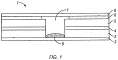
- an electrochemical cell 1 illustrated in a cross sectional side view, comprises a base layer 2 formed from a non -conducting porous material.
- the base layer 2 is preferably formed from PET or a laminated material and has a thickness of 100 - 250 ⁇ m, preferably around 125 ⁇ m.
- a non -conducting supporting layer 3 is formed on the base layer 2.
- the supporting layer 3 is also preferably formed from PET and has a thickness in the range of 100 ⁇ m to 500 ⁇ m, preferably 250 ⁇ m.
- the supporting layer 3 forms a support on which a working electrode 4 is formed.
- the working electrode 4 is preferably in the form of a continuous band around the wall(s) of the cell 1.
- the thickness of the working electrode 4, which is its dimension in a vertical direction when the cell 1 is placed on the base 2, is typically from 0.01 to 50 micro meters. Preferred and other possible thicknesses of the working electrode are as described in our co-pending application WO 03/056319 .
- the working electrode 4 is preferably formed from carbon, for example in the form of conducting ink.
- a preferred carbon based conducting ink comprises a suspension of carbon dispersed in a resin solution.
- the working material may be formed of other materials and inks as detailed in WO 03/056319 . Furthermore, two or more layers of the same or different materials may be used to form the working electrode.
- a dielectric layer 5 comprising an insulating material typically a polymer, a plastic or ceramic again as detailed in WO 03/056319 is formed on and insulates the working electrode 4 from a pseudo-reference or counter electrode 6.
- the dielectric layer 5 is of thickness 1 to 1000 ⁇ m.
- the dielectric layer could be formed of more than one layer.
- the pseudo-reference or counter electrode 6 in a preferred embodiment comprises silver/silver chloride and forms part of the top of the cell 1.
- the material of the counter electrode 6 is provided in the form of a conductive ink and the pseudo-reference electrode 6 has a thickness of the order of 5 microns or greater. A range of possible materials, inks and thicknesses suitable for the pseudo-reference electrode are also discussed in WO 03/056319 .
- the layers are deposited in a layer by layer fashion.
- a working electrode 3 preferably formed of carbon is screen printed on the supporting layer 2 and the dielectric layer 5 is printed on the working electrode 3.
- the dielectric layer 5 may be printed as two layers so that any pin-holes that occur in the first layer of printing are filled.
- the pseudo-reference electrode 6, preferably formed of silver/silver chloride is screen printed on the dielectric layer 5.
- Laser drilling, mechanical punching or other drilling means is used to form a hole 7 through the dielectric layer 5, the working electrode 4 and the supporting layer 3.
- the hole 7 has a diameter of about 0.5 to 1.0 mm.
- the pseudo-reference electrode ends around 0.4 to 0.5mm from the edge of the hole 7.
- the base layer 2 is fixed, for example by a suitable adhesive, to the un-printed side of the supporting layer 3 to produce the base of the cell 1.
- the base layer 2 may take the form of a porous membrane containing air holes so that air in the well can be displaced when a measurement sample is introduced into the well formed by hole 7.
- An electro-active substance 8 is contained within the hole 7.
- the electro-active substance 8 may be freeze dried to form a porous cake.
- a measurement sample not shown
- the electro-active substance 8 resuspends and an electrochemical reaction may occur and a measurable current, voltage or charge may occur in the cell.
- Electro-active substances are discussed in more detail in our co-pending application WO 03/056319 .
- the open end of the cell is covered with a membrane 9 that is permeable to components of the sample to be tested, for example blood.
- the membrane may also be used to filter out components of the sample that should not enter the cell, for example red blood cells.
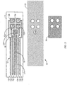
- the sensor strip 10 comprises an insulating substrate sheet 11. Formed on the insulating substrate sheet 11 is a patterned layer 12 of material that forms four working electrodes 12a, 12b, 12c and 12d, one for each of the respective four cells and four conductive tracks 12e, 12f, 12g and 12h each of which in electrical contact with a respective one of the four working electrodes 12a, 12b, 12c and 12d.
- the patterned layer 12 also defines an additional pad 12i, a fifth conductive track 12j in electrical contact with the additional pad 12i and an additional conductive track 12k.
- the patterned layer 12 is formed from carbon and is screen printed on the insulating substrate sheet 11.
- the four cells each further comprises a dielectric insulating layer 13 deposited over the four working electrodes 12a, 12b, 12c and 12d and a pseudo-reference electrode layer 14, in a preferred embodiment formed from silver/ silver chloride and screen printed on the dielectric layer 13.
- the dielectric layer 13 and the pseudo-reference electrode layer 14 are each illustrated shifted laterally sideways from their true positions in the strip 10.
- Each of the four cells further comprises a respective one of four holes 15a, 15b, 15c and 15d formed through the, the dielectric layer 13 its respective working electrode 12a, 12b, 12c and 12d and the supporting layer 11 ending at a base layer (not illustrated).
- a fifth hole 15e is printed on the dielectric layer 13 to the additional pad 12i.
- the pseudo-reference electrode 14 makes electrical contact with the additional pad 12i.
- Each of the four conductive tracks 12e, 12f, 12g and 12h allows the respective working electrode 12a, 12b, 12c and 12d with which it is in electrical contact to be placed in a circuit with the pseudo-reference electrode 14, measuring instruments and voltage sources.
- the fifth conductive track 12j which is in electrical contact with the pseudo-reference electrode 14 via the additional pad 12i, allows the pseudo-reference electrode 14 to be placed in a circuit with any of the four working electrodes 12a, 12b, 12c and 12d, measuring instruments and voltage sources.
- This second conductive layer is preferably deposited before and hence underneath the first, although for reasons of clarity, it is illustrated as being above the first layer in Figure 2 .
- this second conductive layer does not extend underneath any of the four working electrodes 12a, 12b, 12c and 12d or underneath the additional pad 12i.
- the first track layer is carbon and the second is silver an overall track resistance is reduced form around 2 k ⁇ in the absence of the silver to around 200 ⁇ in its presence.
- the additional conductive track 12k is electrically connected to the fifth conductive track 12j, and hence the pseudo-reference electrode 14 by a portion 16 of the second conductive layer.
- a first section 17 of the additional conductive track 12k comprises both the relatively poor conductor, for example carbon and underneath this, the better conductor, for example silver.
- a second section 18 of the additional conductive track 12k comprises the relatively poor conductor only.
- Additional conductive track 12k is used to obtain a measurement I meas of the current that flows through the track 12k when a predetermined voltage, for example 100mv, is applied across the additional track 12k and the fifth conductive track 12j.
- the measurement I meas is indicative of the thickness of the in this example carbon, that forms the second section 18 of the track 12k.
- this measurement is also indicative of the thickness of the carbon working electrodes 12a, 12b, 12c and 12d. These electrodes have the same thickness as the carbon in additional conductive track 12k, as they were deposited at the same time as the additional track 12k and under the same conditions.
- the measured value I meas may then be used in determining a normalising or correction factor F, which during a subsequent test on a sample using more than one of the cells can be used to compensate the current output from a cell for the effect thereon of any variation in the working electrode thickness from a reference thickness.
- I nom is taken as an arbitrary value within limits determined by the sheet thickness. In essence, in this alternative embodiment, I nom is indicative of the thickness of a notional working electrode.
- F will be lower than the value 1 if the thickness of the additional track of the given strip is greater than the average thickness of the additional tracks of the strips in the sample (or greater than the thickness of the notional electrode), F will be higher than the value 1 if the thickness of the additional track of the given strip is less than the average (or less than the thickness of the notional electrode), and F will be equal to the value 1 if the thickness of the additional track of the given strip is equal to the average (or equal to the thickness of the notional electrode).
- the thickness of the deposited additional track is effectively being measured by means of determining the electrical resistance of the track.
- the resulting measurement is used to obtain the correction factor F.
- the obtained correction factor F for a given strip is used to scale the electrochemical current generated by an electrochemical cell of the strip during analysis of an actual sample, for example, a blood sample.
- the meter or measurement apparatus used to measure the electrochemical current may be programmed with the correction factor F for that strip. After measuring the electrochemical current, the meter scales the current with the correction factor to generate a scaled current measurement. The scaled current reading is then used to calculate the concentration of one or more components in the sample.
- each strip (or its packaging) may be provided with a data tag such as bar code encoding the correction factor for that strip and each measuring meter may be provided with a data tag reader, such as a bar code reader.
- a data tag reader such as a bar code reader.
- a user may program values for I nom , K, X and Y into a meter by scanning the relevant bar code with the meter's bar code reader so that the necessary correction can be performed based on I meas .
- the values may be programmed into the meter by other electronic or opto electronic data tag means, for example using RFID or using a ROM chip.
- data from the data tag may be input manually.
- the data tag may be applied to the sensor strip as a part of the manufacturing process, following a parameter measurement stage.
- the processing to obtain the scaling/correction factor may be effected prior to storing the data on the tag or subsequently (for example by the meter).
- the data tag may be representative of a single strip or may be representative of a batch of sensors, for example an array of sensors provided on a substrate sheet.
- correction factor or Imeas value
- the meter detects that a correction factor (or Imeas value) is outside of this range then an error message may be presented to a user, prompting the user to use a fresh strip. The number of strips in a batch that are rejected in this way may be used to evaluate the stability of the ink used to make the strips.
- embodiments of the invention allow the manufacture of sensor strips using the inexpensive techniques referred to in the introduction. Calculating an appropriate correction factor and applying it to a current produced when a sample is tested, compensates the current of the effect of any variation in the measuring parameters working electrode (e.g. thickness) norm value for the parameter for the batch average for the parameter or from the notional norm value for the parameter for the working electrode.
- working electrode e.g. thickness
- meters configured to work with cells having working electrodes of thickness equal to that of the batch average thickness (or the thickness of the notional working electrode) can also work with cells whose working electrode thickness varies from this.
- each of the strips 10 on a sheet is provided with its own additional conductive track 12.
- the conductive tracks 12 and in particular the additional conductive track 12k can have various configurations, and exemplary configurations are shown in Figures 3A to 3E .
- the tracks are deposited in accordance with the embodiment of Figure 2 .
- the additional conductive track 12k is connected to the conductive track 12; which is in electrical conduct with the pseudo reference electrode.
- the additional conductive track 12 forms an extension leg at the free end of the track 12; connected to the pseudo reference electrode.
- a short circuit current flows when a voltage is applied across the track 12 between the points X and Y in the diagram.
- the additional conductive track 12k extends from a free end X in a loop about the working electrodes 12a, 12d and returns to a second free end Y.
- a current flows in track 12k when a voltage is applied across X and Y.
- the arrangement of Figure 3D is generally similar to the arrangement of Figure 3C however the track 12k includes a terminal return portion at one of its free ends.
- a voltage can be applied across X Y or XW to flow current either along a short length of track 12k between X and Y or the longer length between X and W. Generally the results will be most representative of the relevant track parameter when using the longer length track length.
- the track 12 k is entirely separate from the track 12j connected to the pseudo reference (winter) electrode;
- the voltage can be applied across the ends X Y of track 12k or at spaced positions along the length of track 12k.
- Substrate sheets were printed with carbon electrode strip tracks (such as those shown in Figure 3A ). Each sheet had a 126 electrode strips (7 rows, 18 columns).
- Example 1 Variation of sheet resistance with thickness of carbon layer.
- the electrode design was as shown in figure 3a .
- the resistance of each electrode was measured between the exposed carbon legs of the Counter Electrode 12; and extra leg 12k with calibrated multimeter. An average was taken in order to get the average sheet resistance.
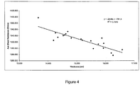
- the thickness of the carbon layer was measured at centre of each sheet using a Mitutuyo surftest SV2000 Tallysurf unit.
- the average sheet resistance was plotted against the carbon thickness at the center of the sheet ( figure 4 ). This shows that there is a correlation between the sheet resistance and the thickness of the carbon layer.
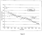
- Example 2 The average sheet resistance was taken for every 2 nd sheet in a batch. The resistance measured with calibrated multimeter between the exposed carbon legs of counter electrode (leg 12; and the extra leg 12k for resistance measurement ( figure 5 ). The average was calculated from array of measurement over a sheet (example show in table 1 below) Table 1: resistance measurements across a sheet.
- Example 3 In order to investigate the relationship between the thickness of the Carbon layer and the resistance of the carbon layer, some PET sheets were printed with different carbon thicknesses. To do so, the carbon printing and drying stages were repeated up to four times. The printed cards thus had 1, 2, 3 or 4 layers of carbon, giving carbon heights of between 17 - 56 ⁇ m.
- the thickness profiles of the printed tracks and pads were measured using a Mitutoyo Surftest SV-2000 talystep.
- the resistance of the spare carbon leg was calculated by measuring the short circuit current using an Autolab PGSTAT12 potentiostat.
- Ru hexaammine solution was deposited in the well and a cyclic voltammogram recorded at 100 mVs -1 .
- Ru Hexaammine Test Solution The Ru hexaammine test solution consisted of 10mM [Ru(NH 3 ) 6 ]Cl 3 (Alfa Aesar, 010511) in Tris pH 9 buffer (Sigma, T-1444) with 100 mM KCl (BDH, 101984L), 50 mM MgSO 4 (Sigma, M-5921) and 1 % Sodium Taurocholate (Sigma T4009-5G) .
- the cards were cut to form wells and the thickness profiles of the carbon spare legs were measured.
- the design was as shown in figure 3a . Strips with different carbon thicknesses were then ruthenium tested according to the protocol described above.
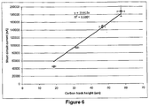
- the graph in Figure 6 presents the variation of the short circuit current as a function of the carbon track height.
- the short circuit measurement is linearly linked to the track and thus to the electrode thickness.
- the electrode thickness compensation allows the global coefficient of variation (CV) to be reduced from 13.89% to 6.4%. The reproducibility is therefore improved thanks to the correction.
- the short circuit current values vary from 47300 to 51200 nA. It corresponds to a variation from 15.0 ⁇ m to 16.3 ⁇ m in carbon thickness.
- Example 4 Resistance compensation implemented via a data tag barcode.
- the barcode may consist of encoded non-variable and variable data associated with a product, for example: Product Code (PPP) Expiry Date (DDMMMYY) Lot/Batch Number (BATCH) Calibration Data (CALIBRATION)
- PPP Product Code
- DDMMMYY Expiry Date
- BATCH Lot/Batch Number
- Calibration Data CALIBRATION
- this barcode will be the same for each strip within a batch.
- the compensation resistance value for the batch will be calculated (for example using the methods shown in example 3) and will be included within the calibration information for the barcode. For example: if a value of 1.975 kOhms is calculated, then the 1975 will be included within the calibration information. This will then be read by an associated electronic device to perform a correction or be looked up against a known curve/equation.
- the batch compensation resistance value will be measured from the additional leg electrode or test-points and calculated prior to printing the product barcode during the manufacturing process.
- each strip could have it own strip barcode with the individual compensation resistance or value.
- Strip Compensation Value Strip Barcode 1 1.975 PPP DDMMMYY 12345 CALIBRA1975 2 1.982 PPP DDMMMYY 12345 CALIBRA1982 3 1.756 PPP DDMMMYY 12345 CALIBRA1756 4 1.888 PPP DDMMMYY 12345 CALIBRA1888 5 1.903 PPP DDMMMYY 12345 CALIBRA1903
- these compensation values will be used by the electronic device to correct via a look up table, curve or equation.
- the manufacturing process may be set up to measure the compensation from an additional strip leg during packaging and print the strip barcode as the individual strip is packed.
Landscapes
- Health & Medical Sciences (AREA)
- Chemical & Material Sciences (AREA)
- Hematology (AREA)
- Life Sciences & Earth Sciences (AREA)
- Analytical Chemistry (AREA)
- Chemical Kinetics & Catalysis (AREA)
- Electrochemistry (AREA)
- Physics & Mathematics (AREA)
- Molecular Biology (AREA)
- Biochemistry (AREA)
- General Health & Medical Sciences (AREA)
- General Physics & Mathematics (AREA)
- Immunology (AREA)
- Pathology (AREA)
- Investigating Or Analyzing Materials By The Use Of Electric Means (AREA)
- Battery Electrode And Active Subsutance (AREA)
Claims (3)
- Procédé de détermination d'un facteur de mise à l'échelle (F) pour la mise à l'échelle d'une sortie d'un capteur (10) comprenant une première cellule électrochimique (1) ayant une électrode de travail (12a) qui est en contact électrique avec une piste conductrice (12e), l'électrode de travail et la piste conductrice étant formées sur un substrat commun, pour compenser l'effet sur la sortie provoqué par une quelconque variation dans l'épaisseur d'une électrode de travail (12a) par rapport à une valeur de référence de l'épaisseur, le procédé comprenant les étapes consistant en :l'obtention d'une première valeur mesurée (Imeas) à partir d'une partie (18) d'une piste conductrice supplémentaire (12k) formée sur le substrat commun de manière à avoir la même épaisseur et formée du même matériau que l'électrode de travail (12a) et déposée en même temps et sous les mêmes conditions que l'électrode de travail (12a) ; etoù la première valeur mesurée est le courant (Imeas) obtenu lorsqu'une tension prédéterminée est appliquée entre la piste supplémentaire (12k) et une autre piste conductrice (12j) également formée sur ledit substrat commun ;la génération du facteur de mise à l'échelle (F) à partir de la première valeur mesurée et d'une seconde valeur mesurée (Inom), où la seconde valeur mesurée se rapporte à l'épaisseur moyenne de l'électrode de travail (12a) d'un lot de cellules (1) et est dépendante de la résistance électrique moyenne d'une pluralité de pistes conductrices supplémentaires (12k), chaque piste conductrice supplémentaire de la pluralité de pistes conductrices supplémentaires (12k) étant formée sur un substrat commun distinct (11) avec une cellule respective des cellules du lot de cellules (1) et formée du même matériau que, et ayant la même épaisseur que, l'électrode de travail (12a) de la cellule respective des cellules du lot de cellules et déposée en même temps et sous les mêmes conditions, où la seconde valeur mesurée pour chaque piste conductrice supplémentaire de la pluralité de pistes conductrices supplémentaires (12k) est obtenue par :l'application d'une tension prédéterminée entre cette piste conductrice supplémentaire (12k) et une autre piste (12j) formée sur chaque substrat commun distinct (11) avec cette piste conductrice supplémentaire pour obtenir une valeur de courant ; etle calcul de la moyenne des valeurs de courant obtenues pour obtenir la seconde valeur mesurée.
- Procédé selon la revendication 1, dans lequel chacune de la pluralité d'autres pistes (12j) est électriquement connectée à une pseudo-électrode de référence (14) d'une cellule respective de la pluralité de cellules (1).
- Procédé de mise à l'échelle d'une mesure d'une sortie d'une cellule électrochimique (1), le procédé comprenant les étapes consistant en :la prise d'une mesure d'une sortie de la cellule électrochimique ;la mise à l'échelle de la mesure à l'aide du facteur de mise à l'échelle (F) obtenu par le procédé selon une quelconque revendication précédente.
Priority Applications (1)
| Application Number | Priority Date | Filing Date | Title |
|---|---|---|---|
| PL06779334T PL1922541T3 (pl) | 2005-09-10 | 2006-09-07 | Sposób wyznaczania współczynnika skalowania sygnału wyjściowego ogniwa elektrochemicznego |
Applications Claiming Priority (2)
| Application Number | Priority Date | Filing Date | Title |
|---|---|---|---|
| GBGB0518527.7A GB0518527D0 (en) | 2005-09-10 | 2005-09-10 | Scaling factor for an output of an electrochemical cell |
| PCT/GB2006/003316 WO2007028998A2 (fr) | 2005-09-10 | 2006-09-07 | Facteur de mise a l'echelle pour une sortie d'une cellule electrochimique |
Publications (2)
| Publication Number | Publication Date |
|---|---|
| EP1922541A2 EP1922541A2 (fr) | 2008-05-21 |
| EP1922541B1 true EP1922541B1 (fr) | 2019-06-26 |
Family
ID=35221295
Family Applications (1)
| Application Number | Title | Priority Date | Filing Date |
|---|---|---|---|
| EP06779334.9A Active EP1922541B1 (fr) | 2005-09-10 | 2006-09-07 | Facteur de mise a l'echelle pour une sortie d'une cellule electrochimique |
Country Status (7)
| Country | Link |
|---|---|
| US (1) | US8239138B2 (fr) |
| EP (1) | EP1922541B1 (fr) |
| JP (1) | JP4969577B2 (fr) |
| ES (1) | ES2744124T3 (fr) |
| GB (1) | GB0518527D0 (fr) |
| PL (1) | PL1922541T3 (fr) |
| WO (1) | WO2007028998A2 (fr) |
Families Citing this family (2)
| Publication number | Priority date | Publication date | Assignee | Title |
|---|---|---|---|---|
| JP6923647B2 (ja) * | 2016-10-24 | 2021-08-25 | エフ.ホフマン−ラ ロシュ アーゲーF. Hoffmann−La Roche Aktiengesellschaft | バイオセンサの導電性エレメントの未補償抵抗の補正方法および装置とシステム |
| US11397161B2 (en) * | 2017-10-11 | 2022-07-26 | Anb Sensors Limited | Calibration electrode |
Citations (1)
| Publication number | Priority date | Publication date | Assignee | Title |
|---|---|---|---|---|
| EP1431758A1 (fr) * | 2001-09-28 | 2004-06-23 | Arkray, Inc. | Instrument de mesure et appareil de mesure de concentration |
Family Cites Families (13)
| Publication number | Priority date | Publication date | Assignee | Title |
|---|---|---|---|---|
| DE4329742C2 (de) | 1993-09-03 | 2003-03-20 | Dieter Haaf | Elektrode zum Messen elektrochemischer Größen einer Probe |
| JPH10253572A (ja) * | 1997-03-07 | 1998-09-25 | Toa Denpa Kogyo Kk | メモリー付き電極を備えた計測装置 |
| JP3702582B2 (ja) * | 1997-06-03 | 2005-10-05 | Nok株式会社 | バイオセンサを用いた測定方法 |
| JP2000019147A (ja) | 1998-07-01 | 2000-01-21 | Nok Corp | 反応生成物測定装置 |
| US7073246B2 (en) * | 1999-10-04 | 2006-07-11 | Roche Diagnostics Operations, Inc. | Method of making a biosensor |
| JP2002156358A (ja) * | 2000-11-20 | 2002-05-31 | Matsushita Electric Ind Co Ltd | バイオセンサ、通知装置、及び測定装置 |
| US6814844B2 (en) * | 2001-08-29 | 2004-11-09 | Roche Diagnostics Corporation | Biosensor with code pattern |
| GB0130684D0 (en) | 2001-12-21 | 2002-02-06 | Oxford Biosensors Ltd | Micro-band electrode |
| JP4217161B2 (ja) * | 2002-03-08 | 2009-01-28 | アークレイ株式会社 | 情報認識機能を有する分析装置、これに用いる分析用具、および分析装置と分析用具のユニット |
| CA2529302C (fr) * | 2003-06-20 | 2011-09-20 | F.Hoffmann-La Roche Ag | Systeme et procede pour coder des informations sur une bande diagnostique utilisee comme biodetecteur |
| EP1642125B1 (fr) | 2003-06-20 | 2017-09-27 | Roche Diabetes Care GmbH | Biocapteur a fonctionnalites electriques multiples |
| US7776559B2 (en) * | 2004-01-22 | 2010-08-17 | Hewlett-Packard Development Company, L.P. | Disposable blood test device |
| US7601299B2 (en) * | 2004-06-18 | 2009-10-13 | Roche Diagnostics Operations, Inc. | System and method for coding information on a biosensor test strip |
-
2005
- 2005-09-10 GB GBGB0518527.7A patent/GB0518527D0/en not_active Ceased
-
2006
- 2006-09-07 JP JP2008529686A patent/JP4969577B2/ja active Active
- 2006-09-07 EP EP06779334.9A patent/EP1922541B1/fr active Active
- 2006-09-07 PL PL06779334T patent/PL1922541T3/pl unknown
- 2006-09-07 ES ES06779334T patent/ES2744124T3/es active Active
- 2006-09-07 US US12/066,068 patent/US8239138B2/en active Active
- 2006-09-07 WO PCT/GB2006/003316 patent/WO2007028998A2/fr not_active Ceased
Patent Citations (1)
| Publication number | Priority date | Publication date | Assignee | Title |
|---|---|---|---|---|
| EP1431758A1 (fr) * | 2001-09-28 | 2004-06-23 | Arkray, Inc. | Instrument de mesure et appareil de mesure de concentration |
Also Published As
| Publication number | Publication date |
|---|---|
| WO2007028998A3 (fr) | 2007-06-28 |
| WO2007028998A2 (fr) | 2007-03-15 |
| US8239138B2 (en) | 2012-08-07 |
| ES2744124T3 (es) | 2020-02-21 |
| US20090093979A1 (en) | 2009-04-09 |
| PL1922541T3 (pl) | 2019-11-29 |
| JP4969577B2 (ja) | 2012-07-04 |
| JP2009508100A (ja) | 2009-02-26 |
| GB0518527D0 (en) | 2005-10-19 |
| EP1922541A2 (fr) | 2008-05-21 |
Similar Documents
| Publication | Publication Date | Title |
|---|---|---|
| US8298389B2 (en) | In vitro analyte sensor, and methods | |
| KR0162623B1 (ko) | 습윤중 마이크로 제작 센서를 분석용으로 사용하기 위한 방법 | |
| EP1600773B1 (fr) | Mesure de substances dans des liquides | |
| EP3032250B1 (fr) | Procédé de mesure de substance et dispositif de mesure employant un biocapteur électrochimique | |
| US8460524B2 (en) | System and methods of chemistry patterning for a multiple well biosensor | |
| US20120241318A1 (en) | System and methods for determining an analyte concentration incorporating a hematocrit correction | |
| US20150082874A1 (en) | Sensor array | |
| EP2232251B1 (fr) | Capteur d'essai à auto-calibrage et son procédé de fabrication | |
| KR20100103483A (ko) | 분석 용구, 분석 장치, 시료 부족의 검지 방법 및 시료 분석 방법 | |
| EP3397954B1 (fr) | Appareil de mesure portatif à utiliser avec une bandelette d'essai analytique de type électrochimique avec des connexions de détection de tension d'électrode | |
| US10073991B2 (en) | Systems and methods for correction of on-strip coding | |
| CN112229884A (zh) | 基于碳糊修饰工艺的维生素检测印刷电极及其制备工艺 | |
| US8239138B2 (en) | Scaling factor for an output of an electrochemical cell | |
| EP0683390A1 (fr) | Electrode ampèrométrique sélective à l'égard des ions | |
| US20060008581A1 (en) | Method of manufacturing an electrochemical sensor | |
| US12265049B2 (en) | Manufacturing method for electrochemical sensor, and electrochemical sensor | |
| CN204165979U (zh) | 电阻结构、辨认信息装置及生物传感器 | |
| US20030087453A1 (en) | Method and device for producing and screening composite arrangements | |
| US6355158B1 (en) | Method of measuring pH | |
| CN206132691U (zh) | 具有代码信息的金属膜试纸 | |
| US20190094170A1 (en) | Analytical test strip with integrated electrical resistor | |
| AU2013204819A1 (en) | Method and apparatus for assay of electrochemical properties |
Legal Events
| Date | Code | Title | Description |
|---|---|---|---|
| PUAI | Public reference made under article 153(3) epc to a published international application that has entered the european phase |
Free format text: ORIGINAL CODE: 0009012 |
|
| 17P | Request for examination filed |
Effective date: 20080304 |
|
| AK | Designated contracting states |
Kind code of ref document: A2 Designated state(s): AT BE BG CH CY CZ DE DK EE ES FI FR GB GR HU IE IS IT LI LT LU LV MC NL PL PT RO SE SI SK TR |
|
| RAP1 | Party data changed (applicant data changed or rights of an application transferred) |
Owner name: F. HOFFMANN-LA ROCHE AG |
|
| RAP1 | Party data changed (applicant data changed or rights of an application transferred) |
Owner name: ROCHE DIAGNOSTICS GMBH Owner name: F. HOFFMANN-LA ROCHE AG |
|
| DAX | Request for extension of the european patent (deleted) | ||
| 17Q | First examination report despatched |
Effective date: 20140828 |
|
| RAP1 | Party data changed (applicant data changed or rights of an application transferred) |
Owner name: F. HOFFMANN-LA ROCHE AG Owner name: ROCHE DIABETES CARE GMBH |
|
| STAA | Information on the status of an ep patent application or granted ep patent |
Free format text: STATUS: EXAMINATION IS IN PROGRESS |
|
| REG | Reference to a national code |
Ref country code: DE Ref legal event code: R079 Ref document number: 602006058214 Country of ref document: DE Free format text: PREVIOUS MAIN CLASS: G01N0027416000 Ipc: G01N0027327000 |
|
| GRAP | Despatch of communication of intention to grant a patent |
Free format text: ORIGINAL CODE: EPIDOSNIGR1 |
|
| STAA | Information on the status of an ep patent application or granted ep patent |
Free format text: STATUS: GRANT OF PATENT IS INTENDED |
|
| RIC1 | Information provided on ipc code assigned before grant |
Ipc: G01N 27/416 20060101ALI20181214BHEP Ipc: G01N 27/327 20060101AFI20181214BHEP |
|
| INTG | Intention to grant announced |
Effective date: 20190118 |
|
| GRAS | Grant fee paid |
Free format text: ORIGINAL CODE: EPIDOSNIGR3 |
|
| GRAA | (expected) grant |
Free format text: ORIGINAL CODE: 0009210 |
|
| STAA | Information on the status of an ep patent application or granted ep patent |
Free format text: STATUS: THE PATENT HAS BEEN GRANTED |
|
| AK | Designated contracting states |
Kind code of ref document: B1 Designated state(s): AT BE BG CH CY CZ DE DK EE ES FI FR GB GR HU IE IS IT LI LT LU LV MC NL PL PT RO SE SI SK TR |
|
| REG | Reference to a national code |
Ref country code: GB Ref legal event code: FG4D |
|
| REG | Reference to a national code |
Ref country code: CH Ref legal event code: EP |
|
| REG | Reference to a national code |
Ref country code: AT Ref legal event code: REF Ref document number: 1148878 Country of ref document: AT Kind code of ref document: T Effective date: 20190715 |
|
| REG | Reference to a national code |
Ref country code: DE Ref legal event code: R096 Ref document number: 602006058214 Country of ref document: DE |
|
| REG | Reference to a national code |
Ref country code: IE Ref legal event code: FG4D |
|
| REG | Reference to a national code |
Ref country code: NL Ref legal event code: FP |
|
| PG25 | Lapsed in a contracting state [announced via postgrant information from national office to epo] |
Ref country code: SE Free format text: LAPSE BECAUSE OF FAILURE TO SUBMIT A TRANSLATION OF THE DESCRIPTION OR TO PAY THE FEE WITHIN THE PRESCRIBED TIME-LIMIT Effective date: 20190626 Ref country code: LT Free format text: LAPSE BECAUSE OF FAILURE TO SUBMIT A TRANSLATION OF THE DESCRIPTION OR TO PAY THE FEE WITHIN THE PRESCRIBED TIME-LIMIT Effective date: 20190626 Ref country code: FI Free format text: LAPSE BECAUSE OF FAILURE TO SUBMIT A TRANSLATION OF THE DESCRIPTION OR TO PAY THE FEE WITHIN THE PRESCRIBED TIME-LIMIT Effective date: 20190626 |
|
| REG | Reference to a national code |
Ref country code: LT Ref legal event code: MG4D |
|
| PG25 | Lapsed in a contracting state [announced via postgrant information from national office to epo] |
Ref country code: GR Free format text: LAPSE BECAUSE OF FAILURE TO SUBMIT A TRANSLATION OF THE DESCRIPTION OR TO PAY THE FEE WITHIN THE PRESCRIBED TIME-LIMIT Effective date: 20190927 Ref country code: BG Free format text: LAPSE BECAUSE OF FAILURE TO SUBMIT A TRANSLATION OF THE DESCRIPTION OR TO PAY THE FEE WITHIN THE PRESCRIBED TIME-LIMIT Effective date: 20190926 Ref country code: LV Free format text: LAPSE BECAUSE OF FAILURE TO SUBMIT A TRANSLATION OF THE DESCRIPTION OR TO PAY THE FEE WITHIN THE PRESCRIBED TIME-LIMIT Effective date: 20190626 |
|
| REG | Reference to a national code |
Ref country code: AT Ref legal event code: MK05 Ref document number: 1148878 Country of ref document: AT Kind code of ref document: T Effective date: 20190626 |
|
| PG25 | Lapsed in a contracting state [announced via postgrant information from national office to epo] |
Ref country code: SK Free format text: LAPSE BECAUSE OF FAILURE TO SUBMIT A TRANSLATION OF THE DESCRIPTION OR TO PAY THE FEE WITHIN THE PRESCRIBED TIME-LIMIT Effective date: 20190626 Ref country code: EE Free format text: LAPSE BECAUSE OF FAILURE TO SUBMIT A TRANSLATION OF THE DESCRIPTION OR TO PAY THE FEE WITHIN THE PRESCRIBED TIME-LIMIT Effective date: 20190626 Ref country code: CZ Free format text: LAPSE BECAUSE OF FAILURE TO SUBMIT A TRANSLATION OF THE DESCRIPTION OR TO PAY THE FEE WITHIN THE PRESCRIBED TIME-LIMIT Effective date: 20190626 Ref country code: AT Free format text: LAPSE BECAUSE OF FAILURE TO SUBMIT A TRANSLATION OF THE DESCRIPTION OR TO PAY THE FEE WITHIN THE PRESCRIBED TIME-LIMIT Effective date: 20190626 Ref country code: RO Free format text: LAPSE BECAUSE OF FAILURE TO SUBMIT A TRANSLATION OF THE DESCRIPTION OR TO PAY THE FEE WITHIN THE PRESCRIBED TIME-LIMIT Effective date: 20190626 Ref country code: PT Free format text: LAPSE BECAUSE OF FAILURE TO SUBMIT A TRANSLATION OF THE DESCRIPTION OR TO PAY THE FEE WITHIN THE PRESCRIBED TIME-LIMIT Effective date: 20191028 |
|
| REG | Reference to a national code |
Ref country code: ES Ref legal event code: FG2A Ref document number: 2744124 Country of ref document: ES Kind code of ref document: T3 Effective date: 20200221 |
|
| PG25 | Lapsed in a contracting state [announced via postgrant information from national office to epo] |
Ref country code: IS Free format text: LAPSE BECAUSE OF FAILURE TO SUBMIT A TRANSLATION OF THE DESCRIPTION OR TO PAY THE FEE WITHIN THE PRESCRIBED TIME-LIMIT Effective date: 20191026 |
|
| PG25 | Lapsed in a contracting state [announced via postgrant information from national office to epo] |
Ref country code: TR Free format text: LAPSE BECAUSE OF FAILURE TO SUBMIT A TRANSLATION OF THE DESCRIPTION OR TO PAY THE FEE WITHIN THE PRESCRIBED TIME-LIMIT Effective date: 20190626 |
|
| PG25 | Lapsed in a contracting state [announced via postgrant information from national office to epo] |
Ref country code: DK Free format text: LAPSE BECAUSE OF FAILURE TO SUBMIT A TRANSLATION OF THE DESCRIPTION OR TO PAY THE FEE WITHIN THE PRESCRIBED TIME-LIMIT Effective date: 20190626 |
|
| PG25 | Lapsed in a contracting state [announced via postgrant information from national office to epo] |
Ref country code: IS Free format text: LAPSE BECAUSE OF FAILURE TO SUBMIT A TRANSLATION OF THE DESCRIPTION OR TO PAY THE FEE WITHIN THE PRESCRIBED TIME-LIMIT Effective date: 20200224 Ref country code: MC Free format text: LAPSE BECAUSE OF FAILURE TO SUBMIT A TRANSLATION OF THE DESCRIPTION OR TO PAY THE FEE WITHIN THE PRESCRIBED TIME-LIMIT Effective date: 20190626 |
|
| REG | Reference to a national code |
Ref country code: CH Ref legal event code: PL |
|
| REG | Reference to a national code |
Ref country code: DE Ref legal event code: R097 Ref document number: 602006058214 Country of ref document: DE |
|
| PLBE | No opposition filed within time limit |
Free format text: ORIGINAL CODE: 0009261 |
|
| STAA | Information on the status of an ep patent application or granted ep patent |
Free format text: STATUS: NO OPPOSITION FILED WITHIN TIME LIMIT |
|
| PG2D | Information on lapse in contracting state deleted |
Ref country code: IS |
|
| PG25 | Lapsed in a contracting state [announced via postgrant information from national office to epo] |
Ref country code: CH Free format text: LAPSE BECAUSE OF NON-PAYMENT OF DUE FEES Effective date: 20190930 Ref country code: LI Free format text: LAPSE BECAUSE OF NON-PAYMENT OF DUE FEES Effective date: 20190930 Ref country code: IE Free format text: LAPSE BECAUSE OF NON-PAYMENT OF DUE FEES Effective date: 20190907 Ref country code: LU Free format text: LAPSE BECAUSE OF NON-PAYMENT OF DUE FEES Effective date: 20190907 |
|
| 26N | No opposition filed |
Effective date: 20200603 |
|
| REG | Reference to a national code |
Ref country code: BE Ref legal event code: MM Effective date: 20190930 |
|
| PG25 | Lapsed in a contracting state [announced via postgrant information from national office to epo] |
Ref country code: BE Free format text: LAPSE BECAUSE OF NON-PAYMENT OF DUE FEES Effective date: 20190930 Ref country code: SI Free format text: LAPSE BECAUSE OF FAILURE TO SUBMIT A TRANSLATION OF THE DESCRIPTION OR TO PAY THE FEE WITHIN THE PRESCRIBED TIME-LIMIT Effective date: 20190626 |
|
| PG25 | Lapsed in a contracting state [announced via postgrant information from national office to epo] |
Ref country code: CY Free format text: LAPSE BECAUSE OF FAILURE TO SUBMIT A TRANSLATION OF THE DESCRIPTION OR TO PAY THE FEE WITHIN THE PRESCRIBED TIME-LIMIT Effective date: 20190626 |
|
| PG25 | Lapsed in a contracting state [announced via postgrant information from national office to epo] |
Ref country code: HU Free format text: LAPSE BECAUSE OF FAILURE TO SUBMIT A TRANSLATION OF THE DESCRIPTION OR TO PAY THE FEE WITHIN THE PRESCRIBED TIME-LIMIT; INVALID AB INITIO Effective date: 20060907 |
|
| PGFP | Annual fee paid to national office [announced via postgrant information from national office to epo] |
Ref country code: NL Payment date: 20250820 Year of fee payment: 20 |
|
| PGFP | Annual fee paid to national office [announced via postgrant information from national office to epo] |
Ref country code: DE Payment date: 20250820 Year of fee payment: 20 |
|
| PGFP | Annual fee paid to national office [announced via postgrant information from national office to epo] |
Ref country code: PL Payment date: 20250820 Year of fee payment: 20 Ref country code: IT Payment date: 20250820 Year of fee payment: 20 |
|
| PGFP | Annual fee paid to national office [announced via postgrant information from national office to epo] |
Ref country code: GB Payment date: 20250820 Year of fee payment: 20 |
|
| PGFP | Annual fee paid to national office [announced via postgrant information from national office to epo] |
Ref country code: FR Payment date: 20250821 Year of fee payment: 20 |
|
| PGFP | Annual fee paid to national office [announced via postgrant information from national office to epo] |
Ref country code: ES Payment date: 20251001 Year of fee payment: 20 |