EP1923739A1 - Optischer Modulator beruhend auf einer M-wertigen Differenz-Phasenumtastung - Google Patents
Optischer Modulator beruhend auf einer M-wertigen Differenz-Phasenumtastung Download PDFInfo
- Publication number
- EP1923739A1 EP1923739A1 EP20070016913 EP07016913A EP1923739A1 EP 1923739 A1 EP1923739 A1 EP 1923739A1 EP 20070016913 EP20070016913 EP 20070016913 EP 07016913 A EP07016913 A EP 07016913A EP 1923739 A1 EP1923739 A1 EP 1923739A1
- Authority
- EP
- European Patent Office
- Prior art keywords
- voltage
- phase
- bias
- shift
- mach
- Prior art date
- Legal status (The legal status is an assumption and is not a legal conclusion. Google has not performed a legal analysis and makes no representation as to the accuracy of the status listed.)
- Withdrawn
Links
Images






Classifications
-
- G—PHYSICS
- G02—OPTICS
- G02F—OPTICAL DEVICES OR ARRANGEMENTS FOR THE CONTROL OF LIGHT BY MODIFICATION OF THE OPTICAL PROPERTIES OF THE MEDIA OF THE ELEMENTS INVOLVED THEREIN; NON-LINEAR OPTICS; FREQUENCY-CHANGING OF LIGHT; OPTICAL LOGIC ELEMENTS; OPTICAL ANALOGUE/DIGITAL CONVERTERS
- G02F1/00—Devices or arrangements for the control of the intensity, colour, phase, polarisation or direction of light arriving from an independent light source, e.g. switching, gating or modulating; Non-linear optics
- G02F1/01—Devices or arrangements for the control of the intensity, colour, phase, polarisation or direction of light arriving from an independent light source, e.g. switching, gating or modulating; Non-linear optics for the control of the intensity, phase, polarisation or colour
- G02F1/21—Devices or arrangements for the control of the intensity, colour, phase, polarisation or direction of light arriving from an independent light source, e.g. switching, gating or modulating; Non-linear optics for the control of the intensity, phase, polarisation or colour by interference
- G02F1/225—Devices or arrangements for the control of the intensity, colour, phase, polarisation or direction of light arriving from an independent light source, e.g. switching, gating or modulating; Non-linear optics for the control of the intensity, phase, polarisation or colour by interference in an optical waveguide structure
- G02F1/2255—Devices or arrangements for the control of the intensity, colour, phase, polarisation or direction of light arriving from an independent light source, e.g. switching, gating or modulating; Non-linear optics for the control of the intensity, phase, polarisation or colour by interference in an optical waveguide structure controlled by a high-frequency electromagnetic component in an electric waveguide structure
-
- G—PHYSICS
- G02—OPTICS
- G02F—OPTICAL DEVICES OR ARRANGEMENTS FOR THE CONTROL OF LIGHT BY MODIFICATION OF THE OPTICAL PROPERTIES OF THE MEDIA OF THE ELEMENTS INVOLVED THEREIN; NON-LINEAR OPTICS; FREQUENCY-CHANGING OF LIGHT; OPTICAL LOGIC ELEMENTS; OPTICAL ANALOGUE/DIGITAL CONVERTERS
- G02F1/00—Devices or arrangements for the control of the intensity, colour, phase, polarisation or direction of light arriving from an independent light source, e.g. switching, gating or modulating; Non-linear optics
- G02F1/01—Devices or arrangements for the control of the intensity, colour, phase, polarisation or direction of light arriving from an independent light source, e.g. switching, gating or modulating; Non-linear optics for the control of the intensity, phase, polarisation or colour
- G02F1/0121—Operation of devices; Circuit arrangements, not otherwise provided for in this subclass
- G02F1/0123—Circuits for the control or stabilisation of the bias voltage, e.g. automatic bias control [ABC] feedback loops
-
- H—ELECTRICITY
- H04—ELECTRIC COMMUNICATION TECHNIQUE
- H04B—TRANSMISSION
- H04B10/00—Transmission systems employing electromagnetic waves other than radio-waves, e.g. infrared, visible or ultraviolet light, or employing corpuscular radiation, e.g. quantum communication
- H04B10/50—Transmitters
- H04B10/516—Details of coding or modulation
- H04B10/548—Phase or frequency modulation
- H04B10/556—Digital modulation, e.g. differential phase shift keying [DPSK] or frequency shift keying [FSK]
- H04B10/5561—Digital phase modulation
-
- H—ELECTRICITY
- H04—ELECTRIC COMMUNICATION TECHNIQUE
- H04L—TRANSMISSION OF DIGITAL INFORMATION, e.g. TELEGRAPHIC COMMUNICATION
- H04L27/00—Modulated-carrier systems
- H04L27/18—Phase-modulated carrier systems, i.e. using phase-shift keying
- H04L27/20—Modulator circuits; Transmitter circuits
- H04L27/2032—Modulator circuits; Transmitter circuits for discrete phase modulation, e.g. in which the phase of the carrier is modulated in a nominally instantaneous manner
- H04L27/2035—Modulator circuits; Transmitter circuits for discrete phase modulation, e.g. in which the phase of the carrier is modulated in a nominally instantaneous manner using a single or unspecified number of carriers
- H04L27/2042—Modulator circuits; Transmitter circuits for discrete phase modulation, e.g. in which the phase of the carrier is modulated in a nominally instantaneous manner using a single or unspecified number of carriers with more than two phase states
- H04L27/205—Modulator circuits; Transmitter circuits for discrete phase modulation, e.g. in which the phase of the carrier is modulated in a nominally instantaneous manner using a single or unspecified number of carriers with more than two phase states in which the data are represented by the change in phase of the carrier
-
- H—ELECTRICITY
- H04—ELECTRIC COMMUNICATION TECHNIQUE
- H04L—TRANSMISSION OF DIGITAL INFORMATION, e.g. TELEGRAPHIC COMMUNICATION
- H04L27/00—Modulated-carrier systems
- H04L27/18—Phase-modulated carrier systems, i.e. using phase-shift keying
- H04L27/20—Modulator circuits; Transmitter circuits
- H04L27/2096—Arrangements for directly or externally modulating an optical carrier
-
- G—PHYSICS
- G02—OPTICS
- G02F—OPTICAL DEVICES OR ARRANGEMENTS FOR THE CONTROL OF LIGHT BY MODIFICATION OF THE OPTICAL PROPERTIES OF THE MEDIA OF THE ELEMENTS INVOLVED THEREIN; NON-LINEAR OPTICS; FREQUENCY-CHANGING OF LIGHT; OPTICAL LOGIC ELEMENTS; OPTICAL ANALOGUE/DIGITAL CONVERTERS
- G02F1/00—Devices or arrangements for the control of the intensity, colour, phase, polarisation or direction of light arriving from an independent light source, e.g. switching, gating or modulating; Non-linear optics
- G02F1/01—Devices or arrangements for the control of the intensity, colour, phase, polarisation or direction of light arriving from an independent light source, e.g. switching, gating or modulating; Non-linear optics for the control of the intensity, phase, polarisation or colour
- G02F1/21—Devices or arrangements for the control of the intensity, colour, phase, polarisation or direction of light arriving from an independent light source, e.g. switching, gating or modulating; Non-linear optics for the control of the intensity, phase, polarisation or colour by interference
- G02F1/212—Mach-Zehnder type
-
- G—PHYSICS
- G02—OPTICS
- G02F—OPTICAL DEVICES OR ARRANGEMENTS FOR THE CONTROL OF LIGHT BY MODIFICATION OF THE OPTICAL PROPERTIES OF THE MEDIA OF THE ELEMENTS INVOLVED THEREIN; NON-LINEAR OPTICS; FREQUENCY-CHANGING OF LIGHT; OPTICAL LOGIC ELEMENTS; OPTICAL ANALOGUE/DIGITAL CONVERTERS
- G02F2203/00—Function characteristic
- G02F2203/20—Intrinsic phase difference, i.e. optical bias, of an optical modulator; Methods for the pre-set thereof
Definitions
- the DQPSK modulation method is a method in which two phase-modulated digital signals are transmitted simultaneously using signal light of one frequency.
- This method requires only half pulse repetition frequencies (for example, 20 GHz) with respect to the speed of data to be transmitted (for example, 40 Gbit/s) and the spectral bandwidth will be half that of the conventional NRZ modulation method, and therefore is superior in frequency utilization efficiency, wavelength dispersion strength, and device transmission properties.
- half pulse repetition frequencies for example, 20 GHz
- the speed of data to be transmitted for example, 40 Gbit/s
- the spectral bandwidth will be half that of the conventional NRZ modulation method, and therefore is superior in frequency utilization efficiency, wavelength dispersion strength, and device transmission properties.
- FIG. 15 is a diagram showing a configuration example of a Mach-Zehnder (hereinafter simply called the MZ type) DQPSK modulator that adopts a conventional DQPSK modulation method.
- MZ type Mach-Zehnder
- a similar DQPSK modulator is also described in Patent Document 1 shown below.
- a DQPSK modulator 100 shown in FIG. 15 is comprised of two child MZ type light modulators 101 and 102, a parent MZ type waveguide 103 comprised of the child MZ type light modulators 101 and 102, and a ⁇ /2 phase shifter 104.
- each of the child MZ type light modulators 101 and 102 comprises MZ type waveguides 101a and 102a, modulating electrodes 101b and 102b, and bias electrodes 101c and 102c adapted to supply a bias voltage to stabilize an operating point.
- light output from an LD (Laser Diode) 105 is input into the childMZ type light modulators 101 and 102.
- Data signals (DATA1, DATA2) output from a DQPSK signal source 106 are amplified by drivers 107 and 108 of differential output and then input into the modulating electrodes 101b and 102b of the child MZ type light modulators 101 and 102 respectively.
- These data signals are thereby to be modulated in the child MZ type light modulators 101 and 102 by the data signals (DATA1, DATA2) from the DQPSK signal source 106 respectively.
- the ⁇ /2 phase shifter 104 performs a phase shift of at least one of signals modulated by the child MZ type light modulators 101 and 102 so that the signals have a phase difference of ⁇ /2 with each other, and the parent MZ type waveguide 103 multiplexes signal lights from the child MZ type light modulators 101 and 102 whose phase shift has been performed by the ⁇ /2 phase shifter 104 so that the light can be output as a DQPSK modulated light.
- continuous light from the LD 105 is modulated by one system of coding data (DATA1) from the DQPSK signal source 106 to output an optical signal carrying information in two optical phases (0 rad or ⁇ rad) (See B in FIG. 16).
- DATA1 continuous light from the LD 105
- DATA2 another system of coding data from the DQPSK signal source 106
- An optical signal carrying information in two optical phases ( ⁇ /2 rad or 3 ⁇ /2 rad) is thereby output (See C in FIG. 16).
- the modulated lights from the child MZ type light modulators 101 and 102 are multiplexed by a multiplexing waveguide constituting the parent MZ type waveguide 103 before being output. That is, by multiplexing the modulated lights from the child MZ type light modulators 101 and 102, the parent MZ type waveguide 103 can output an optical signal carrying information in four optical phases ( ⁇ /4, 3 ⁇ /4, 5 ⁇ /4, and 7 ⁇ /4) with constant light intensity, that is, a DQPSK-modulated optical signal.
- Patent Document 1 describes a DQPSK modulator in which pilot frequency components are provided to a voltage signal supplied to the ⁇ /2 phase shifter 104 and the child MZ type light modulators 101 and 102 to monitor the pilot frequency components in output from the multiplexing waveguide constituting the parent MZ type waveguide 103 to perform feedback control.
- Another obj ect of the present invention is to achieve lower power consumption of the M phase-shift modulator.
- a still another object of the present invention is to achieve simplification of a module configuration.
- a phase-shift voltage to produce a phase shift difference of substantially 2 ⁇ /4 (M) for the n signal lights multiplexed by the multiplexing waveguide can be applied to the two (n) Mach-Zehnder type light modulators together with the driving voltage signal, and therefore a function corresponding to a ⁇ /2 phase shifter in a conventional technique can be added to the two (n) Mach-Zehnder type light modulators and a waveguide space reserved for mounting the ⁇ /2 phase shifter can be left out, achieving reduction in device size.
- electrode lengths can be increased while maintaining the existing device size, and therefore power consumption can advantageously be reduced by lowering the voltage applied to the electrodes.
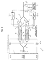
- FIG. 1 is a diagram showing a DQPSK modulator 1 according to the first embodiment of the present invention.
- the DQPSK modulator 1 shown in FIG. 1 comprises a first MZ type light modulator 2, a second MZ type light modulator 3, and a multiplexing waveguide 4, and together with these components, the DQPSK modulator 1 can also be constructed by including a light source 5 composed of LD, a demultiplexing waveguide 6, a DQPSK signal source 7, drivers 8-1 and 8-2, a photo diode (PD) 9, an ABC (Automatic Bias Control) circuit part 10, a phase shift control part 11, bias supply parts 12-1 to 12-3, and a bias-T 13-2.
- a light source 5 composed of LD
- a demultiplexing waveguide 6 a DQPSK signal source 7
- drivers 8-1 and 8-2 drivers 8-1 and 8-2
- PD photo diode
- ABC Automatic Bias Control
- the DQPSK signal source 7 generates original data (DATA1 and DATA2) for modulation as a DQPSK signal light
- the drivers 8-1 and 8-2 amplify electric signals based on (pre-code processed) first data and second data (DATA1, DATA2) from the DQPSK signal source 7 to supply the electric signals to the first MZ type light modulator 2 and second MZ type light modulator 3 as first and second driving electric signals respectively.
- a first driving voltage generating part that generates a first driving voltage signal is constituted by the aforementioned DQPSK signal source 7 and driver 8-1
- a second driving voltage generating part that generates a second driving voltage signal is constituted by the DQPSK signal source 7 and driver 8-2.
- the configuration and operations of the aforementioned DQPSK signal source 7 are described, for example, in PCT National Publication No. 2004-516743.
- the demultiplexing waveguide 6 demultiplexes light from the light source 5 into two, and the first MZ type light modulator 2 can output a first signal light obtained by DPSK-modulating light from the demultiplexing waveguide 6 after applying the first driving voltage signal from the driver 8-1 and has bias electrodes 2c together with a first MZ type optical waveguide 2a to which one output of the demultiplexing waveguide 6 is connected and modulating electrodes 2b adapted to apply the first driving voltage signal.
- the modulating electrodes 2b are a first modulation electrode section adapted to apply the first driving voltage signal in the first MZ type optical waveguide 2a and the bias electrodes 2c are a first bias electrode section adapted to supply a first bias control voltage for bias control when the first driving voltage signal is used for modulation.
- the second MZ type light modulator 3 outputs a second signal light obtained by DPSK-modulating light from the demultiplexing waveguide 6 after applying the second driving voltage signal from the driver 8-2 and has bias electrodes 3c together with a second MZ type optical waveguide 3a to which another output of the demultiplexing waveguide 6 is connected and modulating electrodes 3b adapted to apply the second driving voltage signal. Therefore, the modulating electrodes 3b are a second modulation electrode section adapted to apply the second driving voltage signal in the second MZ type optical waveguide 3a and the bias electrodes 3c are a second bias electrode section adapted to supply a second bias control voltage for bias control when the second driving voltage signal is used for modulation.
- the multiplexing waveguide 4 multiplexes outputs of the first MZ type light modulator 2 and second MZ type light modulator 3, that is, the first and second signal lights DPSK-modulated by the first MZ type light modulator 2 and second MZ type light modulator 3 respectively, and a DQPSK (Differential Quadrature Phase-Shift Keying) -modulated signal light can be output through the multiplexing waveguide 4.
- a DQPSK Different Quadrature Phase-Shift Keying
- the PD 9 monitors power of the DQPSK-modulated signal light output from the multiplexing waveguide 4, and monitoring results are output to the ABC circuit part 10 and the phase shift control part 11. Based on the monitoring results from the PD 9, the ABC circuit part 10 performs feedback control of the bias voltage supplied to the bias electrodes 2c and 3c through the bias supply parts 12-1 and 12-2.
- the ABC circuit part 10 performs feedback control of the bias voltage supplied to the bias electrodes 2c and 3c constituting the first MZ type light modulator 2 and second MZ type light modulator 3 through the bias supply parts 12-1 and 12-2 respectively so that each of the signal lights DPSK-modulated by the first MZ type light modulator 2 and second MZ type light modulator 3 can carry information in one of two phase points (so that operating points are stabilized) having a proper phase difference ( ⁇ phase in this case).
- a technique described in Japanese Patent Application Laid-Open No. HEI 3-251815 or that described in Japanese Patent Application Laid-Open No. 2000-162563 can be applied as a technique to stabilize operating points of the first MZ type light modulator 2 and second MZ type light modulator 3 by the ABC circuit part 10 described above.
- the phase shift control part 11 controls the bias supply part 12-3 to supply the bias voltage for shifting the phase to at least one of the first MZ type light modulator 2 and second MZ type light modulator 3 (in this case, the second MZ type light modulator 3) so that, based on the monitoring results from the PD 9, the signal lights DPSK-modulated by the first MZ type light modulator 2 and second MZ type light modulator 3 have a relatively proper phase difference (in this case, the ⁇ /2 phase) (See C in FIG. 16).
- the bias supply part 12-3 supplies the bias voltage for phase shift to the modulating electrodes 3b of the second MZ type light modulator 3 via the bias-T 13-2, and the aforementioned bias voltage can thereby be supplied to the modulating electrodes 3b formed on each of two arms constituting the second MZ type optical waveguide 3a and thus equivalent phase shifts can be provided to signal lights being propagated through both arms of the second MZ type light modulator 3.
- the bias supply part 12-1 supplies the bias voltage to the bias electrodes 2c so that, under control of the ABC circuit part 10, signal light modulated by the first MZ type light modulator 2 carries information in two phase points having a proper phase difference, that is, having a phase difference of ⁇ (0, ⁇ ) (See B in FIG. 16). Meanwhile, the bias supply part 12-1 may supply the bias voltage through both bias electrodes 2c on two arm waveguides constituting the first MZ type light modulator 2 or through one bias electrode 2c.
- the bias supply part 12-2 supplies the bias voltage to the bias electrodes 2c so that, under control of the ABC circuit part 10, signal light modulated by the second MZ type light modulator 3 carries information in two phase points ( ⁇ /2, 3 ⁇ /2) having a phase difference of ⁇ (See C in FIG. 16). Meanwhile, the bias supply part 12-2 may also supply the bias voltage through both bias electrodes 3c on two modulation waveguides constituting the second MZ type light modulator 3 or through one bias electrode 3c.
- the aforementioned ABC circuit part 10 and the bias supply part 12-1 constitute a first bias control voltage generating part adapted to generate a first bias control voltage for bias control (for stabilization of operating points) when a first driving voltage signal is used for modulation.
- the aforementioned ABC circuit part 10 and the bias supply part 12-2 constitute a second bias control voltage generating part adapted to generate a second bias control voltage for bias control (for stabilization of operating points) when a second driving voltage signal is used for modulation.
- the bias supply part 12-3 outputs the bias voltage to the second MZ type light modulator 3 to shift the phase by ⁇ /2 so that, under control of the phase shift control part 11, signal lights DPSK-modulated by the first MZ type light modulator 2 and second MZ type light modulator 3 have a relatively proper phase difference of ⁇ /2. Then, the bias-T 13-2 superimposes the bias voltage for phase shift from the bias supply part 12-3 on the second driving signal differentially output from the driver 8-2 to be supplied to the modulating electrodes 3b.
- the phase shift control part 11 can stabilize the bias voltage at an optimal control point by dithering and, the aforementioned bias-T 13-2 can superimpose the bias voltage containing low-frequency components for dithering also on the second driving voltage signal (having modulated signal components) from the driver 8-2.
- the phase shift control part 11 can, for example, apply the bias voltage after, for example, low-frequency signals are superimposed by the bias supply part 12-3 to stabilize the bias voltage for phase shift, and also perform feedback control of the bias voltage for phase shift through the bias supply part 12-3 so that applied low-frequency signal components excluding harmonic content contained in monitoring signals output from the PD 9 become maximum.
- a similar technique is described in a specification initially attached to a patent application ( Japanese Patent Application Laid-Open No. 2005-192971 ) submitted by the present applicant.
- the aforementioned PD 9, the phase shift control part 11, and the bias supply part 12-3 constitute a phase-shift voltage generating part adapted to generate a phase-shift voltage so that two signal lights multiplexed by the multiplexing waveguide 4 have a phase shift difference of substantially ⁇ /2
- the bias-T 13-2 constitutes a superimposing part that couples a phase-shift voltage generated by the bias supply part 12-3 to at least one of the first and second driving voltage signals.
- the data signal (DATA1) output from the DQPSK signal source 7 is amplified by the driver 8-1 of differential output and then input into the modulating electrode 2b of the first MZ type light modulator 2 unchanged as a first driving electric signal.
- the data signal (DATA2) output from the DQPSK signal source 7, on the other hand, is amplified by the driver 8-2 of differential output (second driving electric signal) and then, after adding a DC bias for ⁇ /2 phase shift through the bias-T 13-2, input into the modulating electrode 3b of the second MZ type light modulator 3.
- An optical signal output from the light source 5 passes through the first and second MZ type light modulators 2 and 3 and the multiplexing waveguide 4. At this point, the optical signal is phase-modulated by data signals (first and second driving electric signals) output from the drivers 8-1 and 8-2.
- the DC bias feedback-controlled by the ABC circuit part 10 is supplied to the bias electrodes 2c and 3c of the first and second MZ type light modulators 2 and 3 through the bias supply part 12-1 and 12-2 to stabilize operating points of the first and second MZ type light modulators 2 and 3 respectively.
- the DC bias feedback-controlled by the phase shift control part 11 is supplied via the bias supply part 12-3 and the bias-T 13-2 to the modulating electrodes 3b of one of the first and second MZ type light modulators 2 and 3, for example, of the second MZ type light modulator 3 so that the phase difference of an optical signal output from the first MZ type light modulator 2 and that output from the second MZ type light modulator 3 when viewed from the multiplexing waveguide 4 becomes ⁇ /2 with stability.
- the DQPSK modulator 1 is provided with three bias supply parts 12-1 to 12-3, and FIG. 3 exemplifies an algorithm of device control thereof.
- first feedback control of the bias supply part 12-1 and bias supply part 12-2 to supply a bias voltage for determining an operating point of the first MZ type light modulator 2 or second MZ type light modulator 3 is performed by the ABC circuit part 10 (steps S1 and S2).
- the order of control of the bias voltage for the first MZ type light modulator 2 and second MZ type light modulator 3 can be reversed.
- the bias voltage is simultaneously supplied to the two modulating electrodes 3b of the second MZ type light modulator 3 so that the phase difference of an optical signal output from the first MZ type light modulator 2 and that output from the second MZ type light modulator 3 when viewed from the multiplexing waveguide 4 becomes ⁇ /2 with stability through control of the bias supply part 12-3 by the phase shift control part 11 (step S3).
- the bias voltage supplied from the bias supply parts 12-1 to 12-3 can be stabilized by repeating the above-described control (steps S1 to S3) so that quality of DQPSK modulated signals can be maintained.
- a function corresponding to that of the ⁇ /2 phase shifter 104 provided in the parent MZ type waveguide 103 can be added to the modulating electrodes 3b when compared with FIG. 15 shown above, and therefore a waveguide space reserved for mounting the ⁇ /2 phase shifter 104 can now be left out. Therefore, in addition to being able to reduce the device size, by selecting the waveguide space reserved for mounting the ⁇ /2 phase shifter 104 as a formation area of the first and second MZ type light modulators 2 and 3, electrode lengths required for the modulating electrodes 2b and 3b and bias electrodes 2c and 3c can be increased while maintaining the existing device size, advantageously reducing power consumption.
- a bias voltage for phase shift is supplied to the modulating electrodes 3b of the second MZ type light modulator 3 in the first embodiment, but the bias voltage may also be supplied to the modulating electrodes 2b of the first MZ type light modulator 2 by setting up a bias T between the driver 8-1 and modulating electrodes 2b when necessary or to the modulating electrodes 2b and 3b of both the first and second MZ type light modulators 2 and 3.
- bias voltages When a bias voltage is supplied to the modulating electrodes 2b and 3b of both the first and second MZ type light modulators 2 and 3, bias voltages must be set at least in such way that a phase shift amount due to a bias voltage supplied to the modulating electrodes 2b and that due to the bias voltage supplied to the modulating electrodes 3b substantially have a phase difference of ⁇ /2.
- FIG. 4 is a diagram showing a DQPSK modulator 1A according to a first modification of the first embodiment of the present invention.
- the DQPSK modulator 1A shown in FIG. 4 is different from the aforementioned DQPSK modulator 1 shown in FIG. 1 (See numeral 1) in that the bias voltage for phase shift from the bias supply part 12-3 is supplied via the bias electrodes 3c, instead of the modulating electrodes 3b of the second MZ type light modulators 3, but otherwise, the configuration is basically the same as that shown in FIG. 1.
- the same numerals in FIG. 4 as those in FIG. 1 denote approximately the same components.
- the bias electrode 3c is formed on both arms constituting the second MZ type optical waveguide 3a and a bias voltage under control of the phase shift control part 11 is applied to these bias electrodes 3c via the bias supply part 12-3.
- the bias voltage from the bias supply part 12-2 under control of the ABC circuit part 10 is also applied to the bias electrodes 3c, but this bias voltage may be applied to the bias electrodes 3c of both arms or one of the bias electrodes 3c.
- a function corresponding to that of the ⁇ /2 phase shifter 104 (See FIG. 15) can be added to the bias electrodes 3c, and therefore, like the DQPSK modulator 1 shown in FIG. 1, a waveguide space reserved for mounting the ⁇ /2 phase shifter 104 can now be left out to achieve reduction in device size.
- electrode lengths required for the modulating electrodes 2b and 3b and bias electrodes 2c and 3c can be increased while maintaining the existing device size, advantageously reducing power consumption.
- FIG. 5 is a diagram showing a DQPSK modulator 1B according to a second modification of the first embodiment of the present invention.
- the DQPSK modulator 1B shown in FIG. 5 has a bias supply part 12-4 that makes a function of the bias supply part 12-2 and that of the bias supply part 12-3 shareable and is different from the DQPSK modulator 1A shown in FIG. 4 in this respect. Otherwise, the configuration is basically the same as that of the DQPSK modulator 1A shown in FIG. 4 and the same numerals in FIG. 5 as those in FIG. 4 denote approximately the same components.
- a function corresponding to that of the ⁇ /2 phase shifter 104 See FIG. 15
- advantages similar to those of the DQPSK modulator 1 shown in FIG. 1 can be obtained.
- FIG. 6 is a diagram showing a DQPSK modulator 1C according to a third modification of the first embodiment of the present invention.
- the DQPSK modulator 1C shown in FIG. 6 has, instead of the aforementioned bias supply part 12-3 shown in FIG. 4, bias supply parts 12-31 and 12-32 to supply a bias voltage for phase shift to the first and second MZ type light modulators 2 and 3 respectively under control of the phase shift control part 11 and is different from the DQPSK modulator 1A shown in FIG. 4 in this respect.
- the configuration is basically the same as that of the DQPSK modulator 1A shown in FIG. 4 and the same numerals in FIG. 6 as those in FIG. 4 denote approximately the same components.
- the bias electrode 2c is formed on both arms constituting the first MZ type optical waveguide 2a and the bias electrode 3c is formed on both arms constituting the second MZ type optical waveguide 3a.
- the bias supply part 12-31 applies a bias voltage for phase shift to the bias electrodes 2c on both arms constituting the first MZ type optical waveguide 2a under control of the phase shift control part 11 and the bias supply part 12-32 applies a bias voltage for phase shift to the bias electrodes 3c on both arms constituting the second MZ type optical waveguide 3a under control of the phase shift control part 11.
- the bias voltage supplied to the bias electrodes 2c and 3c by the bias supply parts 12-31 and 12-32 respectively is set in such a way that two signal lights output from the first and second MZ type light modulators 2 and 3 to be multiplexed by the multiplexing waveguide 4 have a relative phase difference of ⁇ /2.
- a relative phase difference of two signal lights output from the multiplexing waveguide 4 through the first and second MZ type light modulators 2 and 3 can be ⁇ /2.
- a function corresponding to that of the ⁇ /2 phase shifter 104 (See FIG. 15) can be added to the bias electrodes 2c and 3c, and therefore advantages similar to those of the DQPSK modulator 1 shown in FIG. 1 can be obtained, and the bias voltage required for phase shift can be divided among a plurality of the electrodes 2c and 3c of the MZ type light modulators 2 and 3, further contributing to reduction in power consumption.
- FIG. 7 is a diagram showing a DQPSK modulator 1D according to a fourth modification of the first embodiment of the present invention.
- the DQPSK modulator 1D shown in FIG. 7 has a bias supply part 12-41 that makes a function of the bias supply part 12-1 and that of the bias supply part 12-31 shareable and a bias supply part 12-42 that makes a function of the bias supply part 12-2 and that of the bias supply part 12-32 shareable, and is different from the DQPSK modulator 1C shown in FIG. 6 in this respect.
- the configuration is basically the same as that of the DQPSK modulator 1C shown in FIG. 6 and the same numerals in FIG. 7 as those in FIG. 6 denote approximately the same components.
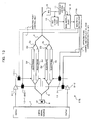
- FIG. 8 is a diagram showing a DQPSK modulator 21 according to a second embodiment of the present invention.
- the DQPSK modulator 21 shown in FIG. 8 is different from the DQPSK modulator 1 in the aforementioned first embodiment in a supply mode of the bias voltage to each of first and second MZ type light modulators 22 and 23 along with the configuration of each of the first and second MZ type light modulators 22 and 23 (See numerals 1 and 2 in FIG. 1). Otherwise, the configuration is basically the same as that of the DQPSK modulator 1 shown in FIG. 1 and the same numerals in FIG. 8 as those in FIG. 1 denote approximately the same components.
- first and second MZ type light modulators 22 and 23 have the first and second MZ type optical waveguides 2a and 3a like the aforementioned first embodiment and also electrodes 2d and 3d for modulation/bias shared use respectively.
- the electrode 2d is formed on both arms constituting the first MZ type optical waveguide 2a and the bias voltage from the bias supply part 12-1 is supplied via the bias-T 13-1 on top of others along with the first driving voltage signal from the driver 8-1.
- the electrode 3d is formed on both arms constituting the second MZ type optical waveguide 3a and the bias voltage from the bias supply parts 12-2 and 12-3 is supplied via the bias-T 13-2 on top of others along with the second driving voltage signal from the driver 8-2.
- the aforementioned electrodes 2d are a first superimposed voltage electrode section adapted to supply a first superimposed voltage in which a first driving voltage signal and a first bias control voltage for bias control for modulation by the first driving voltage signal are superimposed in the first MZ type optical waveguide 2a.
- the electrodes 3d are a second superimposed voltage electrode section adapted to supply a second superimposed voltage in which a second driving voltage signal and a second bias control voltage for bias control for modulation by the second driving voltage signal are superimposed in the second MZ type optical waveguide 3a.
- the aforementioned bias-T 13-1 is a first voltage superimposing part adapted to superimpose a first driving voltage signal generated in the driver 8-1 and a first bias control voltage generated in the bias supply part 12-1 and applies the obtained voltage as a first superimposed voltage to the electrodes 2d as the first superimposed voltage electrode section.
- the bias-T 13-2 is a second voltage superimposing part adapted to superimpose a second driving voltage signal generated in the driver 8-2 and a second bias control voltage generated in the bias supply part 12-2 and applies the obtained voltage as a second superimposed voltage to the electrodes 3d as the second superimposed voltage electrode section. Then, a phase-shift voltage generated in the bias supply part 12-3 is further superimposed on the electrode 3d, which belongs to at least one of the first and second voltage superimposing parts.
- the bias voltage for phase shift can be supplied to the electrode 3d formed on both arms constituting the second MZ type optical waveguide 3a via the bias-T 13-2 in the bias supply part 12-3, equivalent phase shifts can be provided to signal lights propagating through both arms of the second MZ type optical waveguide 3a.
- the first and second MZ type light modulators 22 and 23 are provided with the electrodes 2d and 3d for modulation/bias shared use and accordingly, a waveguide space reserved for forming the bias electrodes 2c and that reserved for forming the bias electrodes 3c in the aforementioned FIG. 1 can be left out to achieve reduction in device size.
- a waveguide space reserved for forming the bias electrodes 2c and 3c in a formation area of the aforementioned electrodes 2d and 3d electrode lengths required for the electrodes 2d and 3d can be increased while maintaining the existing device size, further reducing power consumption.
- the data signal (DATA1) output from the DQPSK signal source 7 is amplified by the driver 8-1 of differential output and then output to the bias-T 13-1 as a first driving electric signal.
- the data signal (DATA2) output from the DQPSK signal source 7, on the other hand, is amplified by the driver 8-2 of differential output and then output to the bias-T 13-2 as a second driving electric signal.
- the first driving voltage signal from the driver 8-1 and the bias voltage for stabilizing operating points from the bias supply part 12-1 under control of the ABC circuit part 10 are superimposed before being supplied to the electrodes 2d.
- the first MZ type light modulator 22 light from the light source 5 is modulated by DATA1 from the DQPSK signal source 7 after stabilizing operating points with the bias voltage from the bias supply part 12-1 before being output as a DPSK-modulated optical signal.
- the second driving voltage signal from the driver 8-2, the bias voltage for stabilizing operating points from the bias supply part 12-2 under control of the ABC circuit part 10, and further the bias voltage for phase shift from the bias supply part 12-3 under control of the phase shift control part 11 are superimposed before being supplied to the electrodes 3d.
- the second MZ type light modulator 23 light from the light source 5 is modulated by DATA2 from the DQPSK signal source 7 after stabilizing the operating points with the bias voltage from the bias supply part 12-2 before being output as a DPSK-modulated optical signal.
- a phase shift can be provided by the bias voltage from the bias supply part 12-3 to the signal light from the second MZ type light modulator 23 to be multiplexed with the signal light from the first MZ type light modulator 22 in the multiplexing waveguide 4 so that the signal light substantially has a phase difference of ⁇ /2 with the signal light from the first MZ type light modulator 22.
- a waveguide space reserved for forming the bias electrodes 2c and that reserved for forming the bias electrodes 3c in the aforementioned FIG. 1 can be left out to achieve reduction in device size.
- electrode lengths required for the electrodes 2d and 3d can be increased while maintaining the existing device size, advantageously reducing power consumption.
- the bias voltage for phase shift is supplied to the electrodes 3d of the second MZ type light modulator 23 in the second embodiment, but may be supplied to the electrodes 2d of the first MZ type light modulator 22 through the bias-T 13-1.
- FIG. 9 is a diagram showing a DQPSK modulator 21A according to a first modification of the second embodiment of the present invention.
- the DQPSK modulator 21A shown in FIG. 9 has, instead of the aforementioned bias supply part 12-3 shown in FIG. 8, a bias supply part 12-33 to supply a bias voltage for phase shift to the first and second MZ type light modulators 22 and 23 respectively under control of the phase shift control part 11 and is different from the DQPSK modulator 21 shown in FIG. 8 in this respect.
- the configuration is basically the same as that of the DQPSK modulator 21 shown in FIG. 8 and the same numerals in FIG. 9 as those in FIG. 8 denote approximately the same components.
- the bias supply part 12-33 applies, under control of the phase shift control part 11 a bias voltage for phase shift to the electrodes 2d formed on both arms constituting the first MZ waveguide 2a and a bias voltage for phase shift to the electrodes 3d formed on both arms constituting the second MZ waveguide 3a.
- the bias voltage to be supplied to the electrodes 2d and the electrodes 3d respectively are set by the bias supply part 12-33 in such a way that two signal lights output from the first and second MZ type light modulators 22 and 23 to be multiplexed by the multiplexing waveguide 4 have a relative phase difference of ⁇ /2.
- a relative phase difference of two signal lights output from the multiplexing waveguide 4 through the first and second MZ type light modulators 22 and 23 can be ⁇ /2.
- allocation of the phase shift amounts to the first and second MZ type light modulators 22 and 23 may be reversed.
- the bias voltage required for phase shift can be divided among a plurality of the electrodes 2d and 3d of the MZ type light modulators 22 and 23, further contributing to reduction in power consumption.
- FIG. 11 is a diagram showing a DQPSK modulator 21C according to a second modification of the second embodiment of the present invention.
- the DQPSK modulator 21C shown in FIG. 11 is obtained by adding a bias ratio setting part 14 to the configuration of the aforementioned DQPSK modulator 21 shown in FIG. 8.
- the bias ratio setting part 14 corrects a deviation of a bias supply ratio due to individual differences for the two electrodes 3d to which a bias voltage for phase shift is supplied.
- the allocation (bias ratio) of the bias voltage from the bias supply part 12-3 can thereby be set by the bias ratio setting part 14 to correct, based on these measurement results, a deviation of the bias supply ratio.
- the bias voltage whose bias ratio is set by the bias ratio setting part 14 is supplied to the corresponding electrode 3d via the bias-T 13-2.
- the aforementioned bias ratio setting part 14 is an application ratio setting part that sets the application ratio of a phase-shift voltage supplied to two electrodes 2d and 3d in each of the first and second Mach-Zehnder type light modulators 22 and 23.
- the DQPSK modulator 21C constructed as described above is provided with the bias ratio setting part 14, and therefore a deviation from ⁇ /2 can be corrected by reducing a difference in bias supply ratio due to, for example, a loss between the two electrodes 3d of the second MZ type light modulator 23.
- the configuration of the bias ratio setting part 14 can also be applied to the DQPSK modulators 21A and 21B shown in FIG. 9 and FIG. 10 respectively.
- a bias ratio setting part 14a as an application ratio setting part may be added to the configuration of the DQPSK modulator 21B shown in FIG. 10.
- the bias ratio setting part 14a shown in FIG. 12 corrects a deviation of the bias supply ratio due to individual differences for the two electrodes 2d and 3d each in the first and second MZ type light modulators 22 and 23 to which a bias voltage for phase shift is supplied.
- the allocation (bias ratio) of the bias voltage from the bias supply part 12-34 can thereby be set by the bias ratio setting part 14a to correct, based on these measurement results, a deviation of the bias supply ratio.
- the bias ratio setting part 14a is provided and therefore a deviation from ⁇ /2 can be corrected by reducing a difference in bias supply ratio due to, for example, a loss between the two electrodes 2d and 3d each of the first and second MZ type light modulators 22 and 23.
- FIG. 13 is a diagram showing a DQPSK modulator 21E according to a third modification of the second embodiment of the present invention.
- the DQPSK modulator 21E shown in FIG. 13 is provided with a bias supply part 12-5 that makes the bias supply parts 12-1 to 12-3 in the aforementioned DQPSK modulator 21 shown in FIG. 8 shareable and also a bias ratio setting part 14b as an application ratio setting part, and is different from the aforementioned DQPSK modulator 21 shown in FIG. 8 in this respect.
- the configuration is basically the same as that of the DQPSK modulator 21 shown in FIG. 8 and the same numerals in FIG. 13 as those in FIG. 8 denote approximately the same components.
- the bias supply part 12-5 outputs a bias voltage for operating point control for the first and second MZ light modulators 22 and 23 based on control from the ABC control part 10 and also that for phase shift for the second MZ light modulator 23 based on control from the phase shift control part 11, and the bias ratio setting part 14b divides the bias voltage signal from the bias supply part 12-5 as a bias voltage signal to the two electrodes 2d and 3d each in the first and second MZ type light modulators 22 and 23 by setting the bias ratio in accordance with individual differences of the electrodes 2d and 3d.
- the bias voltage signal from the bias supply part 12-5 is divided into a bias voltage for operating point control for the first MZ type light modulator 22 and a bias voltage signal for operating point control and phase shift for the second MZ type light modulator 23, and further allocation (bias ratio) of the bias voltage from the bias supply part 12-5 is set to correct a deviation of the bias supply ratio based on individual differences of the two electrodes 2d and 3d each.
- the bias voltage whose bias ratio is set by the bias ratio setting part 14b is supplied to the corresponding electrode 2d via the bias-T 13-1 and to the corresponding electrode 3d via the bias-T 13-2.
- bias supply part made shareable as described above and that of the bias ratio setting part can be applied to the aforementioned DQPSK modulators 21A and 21B shown in FIG. 9 and FIG. 10 respectively.
- a bias supply part 12-6 that makes the bias supply parts 12-1, 12-2, and 12-33 in the DQPSK modulator 21A shown in FIG. 9 shareable may be provided and also a bias ratio setting part 14c may be provided as an application ratio setting part.
- the bias supply part 12-6 outputs a bias voltage for operating point control for the first and second MZ type light modulators 22 and 23 based on control from the ABC circuit part 10 and also that for phase shift for the first and second MZ type light modulators 22 and 23 based on control from the phase shift control part 11, and the bias ratio setting part 14c divides the bias voltage signal from the bias supply part 12-6 as a bias voltage signal to the two electrodes 2d and 3d each in the first and second MZ type light modulators 22 and 23 by setting the bias ratio in accordance with individual differences of the electrodes 2d and 3d.
- allocation (bias ratio) of the bias voltage from the bias supply part 12-6 is set to correct a deviation of the bias supply ratio based on individual differences of the two electrodes 2d and 3d each.
- the bias voltage whose bias ratio is set by the bias ratio setting part 14c is supplied to the corresponding electrode 2d via the bias-T 13-1 and to the corresponding electrode 3d via the bias-T 13-2.
- the bias ratio setting part 14a is provided and therefore a deviation from ⁇ /2 can be corrected by reducing a difference in bias supply ratio due to, for example, a loss between the two electrodes 2d and 3d each of the first and second MZ type light modulators 22 and 23.
- Configurations of the bias ratio setting part as an application ratio setting part shown in FIG. 11 to FIG. 14 can also be applied to each configuration of the first embodiment when necessary.
Landscapes
- Physics & Mathematics (AREA)
- Nonlinear Science (AREA)
- Engineering & Computer Science (AREA)
- Computer Networks & Wireless Communication (AREA)
- Signal Processing (AREA)
- Electromagnetism (AREA)
- General Physics & Mathematics (AREA)
- Optics & Photonics (AREA)
- Optical Modulation, Optical Deflection, Nonlinear Optics, Optical Demodulation, Optical Logic Elements (AREA)
- Optical Communication System (AREA)
Applications Claiming Priority (1)
| Application Number | Priority Date | Filing Date | Title |
|---|---|---|---|
| JP2006308029A JP5055968B2 (ja) | 2006-11-14 | 2006-11-14 | 差動4位相偏移変調器 |
Publications (1)
| Publication Number | Publication Date |
|---|---|
| EP1923739A1 true EP1923739A1 (de) | 2008-05-21 |
Family
ID=39052700
Family Applications (1)
| Application Number | Title | Priority Date | Filing Date |
|---|---|---|---|
| EP20070016913 Withdrawn EP1923739A1 (de) | 2006-11-14 | 2007-08-29 | Optischer Modulator beruhend auf einer M-wertigen Differenz-Phasenumtastung |
Country Status (3)
| Country | Link |
|---|---|
| US (1) | US7840141B2 (de) |
| EP (1) | EP1923739A1 (de) |
| JP (1) | JP5055968B2 (de) |
Cited By (6)
| Publication number | Priority date | Publication date | Assignee | Title |
|---|---|---|---|---|
| EP2169851A3 (de) * | 2008-09-26 | 2010-05-05 | Fujitsu Limited | Optischer Signalgeber |
| EP2282423A1 (de) * | 2009-07-17 | 2011-02-09 | Mitsubishi Electric Corporation | Mehrwertiger optischer Sender |
| EP2296298A4 (de) * | 2008-06-20 | 2012-02-22 | Huawei Tech Co Ltd | Verfahren und vorrichtung zur erzeugung optischer signale |
| US20120106888A1 (en) * | 2009-07-10 | 2012-05-03 | Nippon Telegraph And Telephone Corporation | Optical modulator |
| EP2487524A4 (de) * | 2009-10-09 | 2014-07-09 | Nec Corp | Optisches modulatormodul und verfahren zur modulierung optischer signale |
| WO2015154813A1 (en) * | 2014-04-10 | 2015-10-15 | Fraunhofer-Gesellschaft zur Förderung der angewandten Forschung e.V. | Mach-zehnder modulator and method for operating a mach-zehnder modulator |
Families Citing this family (25)
| Publication number | Priority date | Publication date | Assignee | Title |
|---|---|---|---|---|
| JP4631006B2 (ja) * | 2005-08-24 | 2011-02-16 | 独立行政法人情報通信研究機構 | Fsk変調器の自動調整システム |
| US8687981B2 (en) | 2007-10-02 | 2014-04-01 | Luxtera, Inc. | Method and system for split voltage domain transmitter circuits |
| US8155534B2 (en) * | 2008-06-30 | 2012-04-10 | Alcatel Lucent | Optical modulator for higher-order modulation |
| JP2010028741A (ja) * | 2008-07-24 | 2010-02-04 | Yokogawa Electric Corp | 光送信装置 |
| JP5050003B2 (ja) * | 2008-11-19 | 2012-10-17 | アンリツ株式会社 | 光変調器 |
| JP2010130323A (ja) * | 2008-11-27 | 2010-06-10 | Yokogawa Electric Corp | 光伝送装置 |
| JP5439838B2 (ja) | 2009-02-10 | 2014-03-12 | 富士通オプティカルコンポーネンツ株式会社 | 光変調器 |
| JP5326624B2 (ja) | 2009-02-10 | 2013-10-30 | 富士通オプティカルコンポーネンツ株式会社 | 光変調器 |
| JP5487774B2 (ja) * | 2009-07-27 | 2014-05-07 | 富士通オプティカルコンポーネンツ株式会社 | 光デバイスおよび光送信機 |
| WO2011030763A1 (ja) * | 2009-09-08 | 2011-03-17 | 日本電信電話株式会社 | 光信号送信器、及びバイアス電圧制御方法 |
| JP5267476B2 (ja) * | 2010-01-29 | 2013-08-21 | 富士通オプティカルコンポーネンツ株式会社 | 光デバイスおよび光送信装置 |
| US20110229149A1 (en) * | 2010-03-22 | 2011-09-22 | Infinera Corporation | Optical transmitter supplying optical signals having multiple modulation formats |
| JP5821250B2 (ja) * | 2010-11-19 | 2015-11-24 | 富士通オプティカルコンポーネンツ株式会社 | 光変調装置および光変調制御方法 |
| JP5853386B2 (ja) | 2010-12-16 | 2016-02-09 | 富士通オプティカルコンポーネンツ株式会社 | 光変調装置および光変調制御方法 |
| JP5694089B2 (ja) * | 2011-08-25 | 2015-04-01 | 日本電信電話株式会社 | 光サブキャリア生成器 |
| JP2013122546A (ja) * | 2011-12-12 | 2013-06-20 | Sumitomo Electric Ind Ltd | 半導体光位相変調器及びその駆動方法 |
| US9344194B2 (en) * | 2013-02-21 | 2016-05-17 | Fujitsu Limited | System and method for monitoring and control of an optical modulator for an M-QAM transmitter |
| WO2015120449A2 (en) * | 2014-02-10 | 2015-08-13 | Coriant Advanced Technology, LLC | Distributed traveling-wave mach-zehnder modulator driver |
| CN111181654B (zh) * | 2014-03-20 | 2023-02-28 | 艾里尔大学研究与开发有限公司 | 用于控制信号相位的方法、系统及其应用设备 |
| JP6403276B2 (ja) * | 2015-06-17 | 2018-10-10 | 日本電信電話株式会社 | 光位相変調装置 |
| EP3360247B1 (de) | 2015-10-08 | 2020-12-09 | Ariel-University Research and Development Company Ltd. | Verfahren und system zur steuerung der phase eines signals |
| JP2017116746A (ja) * | 2015-12-24 | 2017-06-29 | 富士通株式会社 | 光送信器及び制御方法 |
| JP6627640B2 (ja) * | 2016-05-16 | 2020-01-08 | 富士通株式会社 | 光送信機 |
| US10547389B2 (en) * | 2016-09-30 | 2020-01-28 | Mitsubishi Electric Corporation | Optical modulation unit, and method for controlling optical modulation unit |
| US10551714B2 (en) * | 2017-05-17 | 2020-02-04 | Finisar Sweden Ab | Optical device |
Citations (5)
| Publication number | Priority date | Publication date | Assignee | Title |
|---|---|---|---|---|
| US4893352A (en) | 1987-06-30 | 1990-01-09 | Massachusetts Institute Of Technology | Optical transmitter of modulated signals |
| WO2002051041A2 (en) * | 2000-12-21 | 2002-06-27 | Bookham Technology Plc. | Improvements in, or relating to, optical communications |
| US20030102938A1 (en) | 2001-11-30 | 2003-06-05 | Hernan Erlig | Photonic RF phase shifter with mitigated RF power fluctuation and devices incorporating the same |
| WO2003049333A1 (en) * | 2001-11-30 | 2003-06-12 | Bookham Technology Plc | Modulation control |
| EP1727303A2 (de) * | 2005-05-23 | 2006-11-29 | Fujitsu Limited | Optische Sendervorrichtung, optische Empfangsvorrichtung und diese enthaltendes Kommunikationssystem |
Family Cites Families (8)
| Publication number | Priority date | Publication date | Assignee | Title |
|---|---|---|---|---|
| JP2642499B2 (ja) | 1990-03-01 | 1997-08-20 | 富士通株式会社 | 光送信器、光変調器の制御回路および光変調方法 |
| DE69127840T2 (de) | 1990-03-01 | 1998-03-05 | Fujitsu Ltd | Optischer Sender |
| US5568614A (en) | 1994-07-29 | 1996-10-22 | International Business Machines Corporation | Data streaming between peer subsystems of a computer system |
| JP3723358B2 (ja) | 1998-11-25 | 2005-12-07 | 富士通株式会社 | 光変調装置及び光変調器の制御方法 |
| JP3999425B2 (ja) * | 1999-11-19 | 2007-10-31 | 日本放送協会 | 高周波信号の光ファイバ伝送用送信機 |
| JP4646048B2 (ja) * | 2001-03-02 | 2011-03-09 | 日本電気株式会社 | 単一側波帯信号光の生成方法および単一側波帯信号光の生成回路 |
| US7346283B2 (en) * | 2004-06-30 | 2008-03-18 | Lucent Technologies Inc. | Method and apparatus for CRZ-DQPSK optical signal generation |
| CN1893324A (zh) * | 2005-07-08 | 2007-01-10 | 富士通株式会社 | 光dqpsk接收机的相位监测装置、相位控制装置及其方法 |
-
2006
- 2006-11-14 JP JP2006308029A patent/JP5055968B2/ja not_active Expired - Fee Related
-
2007
- 2007-08-27 US US11/845,251 patent/US7840141B2/en not_active Expired - Fee Related
- 2007-08-29 EP EP20070016913 patent/EP1923739A1/de not_active Withdrawn
Patent Citations (5)
| Publication number | Priority date | Publication date | Assignee | Title |
|---|---|---|---|---|
| US4893352A (en) | 1987-06-30 | 1990-01-09 | Massachusetts Institute Of Technology | Optical transmitter of modulated signals |
| WO2002051041A2 (en) * | 2000-12-21 | 2002-06-27 | Bookham Technology Plc. | Improvements in, or relating to, optical communications |
| US20030102938A1 (en) | 2001-11-30 | 2003-06-05 | Hernan Erlig | Photonic RF phase shifter with mitigated RF power fluctuation and devices incorporating the same |
| WO2003049333A1 (en) * | 2001-11-30 | 2003-06-12 | Bookham Technology Plc | Modulation control |
| EP1727303A2 (de) * | 2005-05-23 | 2006-11-29 | Fujitsu Limited | Optische Sendervorrichtung, optische Empfangsvorrichtung und diese enthaltendes Kommunikationssystem |
Non-Patent Citations (2)
| Title |
|---|
| S. M. BILAL ET AL: "Automatic bias control of Mach-Zehnder modulators for QPSK and QAM systems", JOURNAL OF OPTICAL TECHNOLOGY, vol. 81, no. 7, 1 July 2014 (2014-07-01), pages 403, XP055184062, ISSN: 1070-9762, DOI: 10.1364/JOT.81.000403 * |
| TAMURA K ET AL: "Phase-noise-canceled differential phase-shift-keying (PNC-DPSK) for coherent optical communication systems", JOURNAL OF LIGHTWAVE TECHNOLOGY USA, vol. 8, no. 2, February 1990 (1990-02-01), pages 190 - 201, XP000103805, ISSN: 0733-8724, DOI: 10.1109/50.47871 * |
Cited By (11)
| Publication number | Priority date | Publication date | Assignee | Title |
|---|---|---|---|---|
| EP2296298A4 (de) * | 2008-06-20 | 2012-02-22 | Huawei Tech Co Ltd | Verfahren und vorrichtung zur erzeugung optischer signale |
| US8831440B2 (en) | 2008-06-20 | 2014-09-09 | Huawei Technologies Co., Ltd. | Method and device for generating optical signals |
| EP2169851A3 (de) * | 2008-09-26 | 2010-05-05 | Fujitsu Limited | Optischer Signalgeber |
| US9419720B2 (en) | 2008-09-26 | 2016-08-16 | Fujitsu Limited | Optical signal transmitter |
| US20120106888A1 (en) * | 2009-07-10 | 2012-05-03 | Nippon Telegraph And Telephone Corporation | Optical modulator |
| EP2453295A4 (de) * | 2009-07-10 | 2012-09-26 | Nippon Telegraph & Telephone | Optischer modulator |
| US8965146B2 (en) * | 2009-07-10 | 2015-02-24 | Nippon Telegraph And Telephone Corporation | Advanced-format optical modulator with low power consumption and low-loss characteristics |
| EP2282423A1 (de) * | 2009-07-17 | 2011-02-09 | Mitsubishi Electric Corporation | Mehrwertiger optischer Sender |
| US8463138B2 (en) | 2009-07-17 | 2013-06-11 | Mitsubishi Electric Corporation | Multi-value optical transmitter |
| EP2487524A4 (de) * | 2009-10-09 | 2014-07-09 | Nec Corp | Optisches modulatormodul und verfahren zur modulierung optischer signale |
| WO2015154813A1 (en) * | 2014-04-10 | 2015-10-15 | Fraunhofer-Gesellschaft zur Förderung der angewandten Forschung e.V. | Mach-zehnder modulator and method for operating a mach-zehnder modulator |
Also Published As
| Publication number | Publication date |
|---|---|
| US20080112710A1 (en) | 2008-05-15 |
| JP5055968B2 (ja) | 2012-10-24 |
| JP2008122786A (ja) | 2008-05-29 |
| US7840141B2 (en) | 2010-11-23 |
Similar Documents
| Publication | Publication Date | Title |
|---|---|---|
| EP1923739A1 (de) | Optischer Modulator beruhend auf einer M-wertigen Differenz-Phasenumtastung | |
| JP5211528B2 (ja) | 光変調装置および光変調方式切替方法 | |
| JP4893637B2 (ja) | 光送信装置およびその制御方法 | |
| JP5476697B2 (ja) | 光信号送信装置 | |
| EP1906564B1 (de) | Optischer Sender | |
| CN101958863B (zh) | 多值光发送器 | |
| JP4522417B2 (ja) | 光変調装置および光変調方法 | |
| US8412047B2 (en) | Polarization multiplexed light transmitter and control method thereof | |
| JP5287239B2 (ja) | 差動4位相偏移変調器およびその位相シフト量制御方法 | |
| JP2010057106A (ja) | 制御装置,偏波多重光変調器,光送信装置および偏波多重光変調器の制御方法 | |
| JP2009033658A (ja) | 光変調装置および光変調方法ならびに光送信装置 | |
| JP6805687B2 (ja) | 光モジュールおよび光変調器のバイアス制御方法 | |
| US9337936B2 (en) | Optical transmission apparatus, optical transmission method and program for optical transmission | |
| JP2016102870A (ja) | 光送信機、及び光変調器のバイアス制御方法 | |
| JP2016045340A (ja) | 光通信装置及び光変調器の制御方法 | |
| JP5321591B2 (ja) | 光送信装置、光受信装置および光通信システム | |
| JP2008066849A (ja) | 光送信機およびその駆動方法 | |
| JP6507524B2 (ja) | 光通信装置及び光変調器の制御方法 | |
| US20120082467A1 (en) | Optical transmitter, optical transmission device, and method of controlling optical transmitter | |
| Zhao et al. | 40G QPSK and DQPSK modulation | |
| JP5030205B2 (ja) | 波長安定化装置および波長安定化方法 | |
| JPH09321709A (ja) | 光送信器 | |
| CN1731710A (zh) | 相位自动校准的多码型可调发射机 |
Legal Events
| Date | Code | Title | Description |
|---|---|---|---|
| PUAI | Public reference made under article 153(3) epc to a published international application that has entered the european phase |
Free format text: ORIGINAL CODE: 0009012 |
|
| AK | Designated contracting states |
Kind code of ref document: A1 Designated state(s): AT BE BG CH CY CZ DE DK EE ES FI FR GB GR HU IE IS IT LI LT LU LV MC MT NL PL PT RO SE SI SK TR |
|
| AX | Request for extension of the european patent |
Extension state: AL BA HR MK RS |
|
| 17P | Request for examination filed |
Effective date: 20081121 |
|
| 17Q | First examination report despatched |
Effective date: 20081219 |
|
| AKX | Designation fees paid |
Designated state(s): DE FR GB |
|
| GRAP | Despatch of communication of intention to grant a patent |
Free format text: ORIGINAL CODE: EPIDOSNIGR1 |
|
| RIC1 | Information provided on ipc code assigned before grant |
Ipc: G02F 1/225 20060101AFI20151029BHEP Ipc: G02F 1/01 20060101ALI20151029BHEP Ipc: H01L 27/20 20060101ALI20151029BHEP |
|
| INTG | Intention to grant announced |
Effective date: 20151123 |
|
| 18D | Application deemed to be withdrawn |
Effective date: 20160405 |