EP1928038B1 - Organischer Dünnfilmtransistor mit Doppelschichtelektroden - Google Patents
Organischer Dünnfilmtransistor mit Doppelschichtelektroden Download PDFInfo
- Publication number
- EP1928038B1 EP1928038B1 EP07121765.7A EP07121765A EP1928038B1 EP 1928038 B1 EP1928038 B1 EP 1928038B1 EP 07121765 A EP07121765 A EP 07121765A EP 1928038 B1 EP1928038 B1 EP 1928038B1
- Authority
- EP
- European Patent Office
- Prior art keywords
- layer
- film transistor
- semiconductor layer
- thin
- source electrode
- Prior art date
- Legal status (The legal status is an assumption and is not a legal conclusion. Google has not performed a legal analysis and makes no representation as to the accuracy of the status listed.)
- Active
Links
Images
Classifications
-
- H—ELECTRICITY
- H10—SEMICONDUCTOR DEVICES; ELECTRIC SOLID-STATE DEVICES NOT OTHERWISE PROVIDED FOR
- H10K—ORGANIC ELECTRIC SOLID-STATE DEVICES
- H10K10/00—Organic devices specially adapted for rectifying, amplifying, oscillating or switching; Organic capacitors or resistors having potential barriers
- H10K10/80—Constructional details
- H10K10/82—Electrodes
- H10K10/84—Ohmic electrodes, e.g. source or drain electrodes
-
- H—ELECTRICITY
- H10—SEMICONDUCTOR DEVICES; ELECTRIC SOLID-STATE DEVICES NOT OTHERWISE PROVIDED FOR
- H10D—INORGANIC ELECTRIC SEMICONDUCTOR DEVICES
- H10D30/00—Field-effect transistors [FET]
- H10D30/60—Insulated-gate field-effect transistors [IGFET]
- H10D30/67—Thin-film transistors [TFT]
- H10D30/6729—Thin-film transistors [TFT] characterised by the electrodes
- H10D30/6737—Thin-film transistors [TFT] characterised by the electrodes characterised by the electrode materials
-
- H—ELECTRICITY
- H10—SEMICONDUCTOR DEVICES; ELECTRIC SOLID-STATE DEVICES NOT OTHERWISE PROVIDED FOR
- H10K—ORGANIC ELECTRIC SOLID-STATE DEVICES
- H10K10/00—Organic devices specially adapted for rectifying, amplifying, oscillating or switching; Organic capacitors or resistors having potential barriers
- H10K10/40—Organic transistors
- H10K10/46—Field-effect transistors, e.g. organic thin-film transistors [OTFT]
- H10K10/462—Insulated gate field-effect transistors [IGFETs]
- H10K10/464—Lateral top-gate IGFETs comprising only a single gate
-
- H—ELECTRICITY
- H10—SEMICONDUCTOR DEVICES; ELECTRIC SOLID-STATE DEVICES NOT OTHERWISE PROVIDED FOR
- H10K—ORGANIC ELECTRIC SOLID-STATE DEVICES
- H10K10/00—Organic devices specially adapted for rectifying, amplifying, oscillating or switching; Organic capacitors or resistors having potential barriers
- H10K10/40—Organic transistors
- H10K10/46—Field-effect transistors, e.g. organic thin-film transistors [OTFT]
- H10K10/462—Insulated gate field-effect transistors [IGFETs]
- H10K10/466—Lateral bottom-gate IGFETs comprising only a single gate
-
- H—ELECTRICITY
- H10—SEMICONDUCTOR DEVICES; ELECTRIC SOLID-STATE DEVICES NOT OTHERWISE PROVIDED FOR
- H10K—ORGANIC ELECTRIC SOLID-STATE DEVICES
- H10K10/00—Organic devices specially adapted for rectifying, amplifying, oscillating or switching; Organic capacitors or resistors having potential barriers
- H10K10/40—Organic transistors
- H10K10/46—Field-effect transistors, e.g. organic thin-film transistors [OTFT]
- H10K10/462—Insulated gate field-effect transistors [IGFETs]
- H10K10/468—Insulated gate field-effect transistors [IGFETs] characterised by the gate dielectrics
- H10K10/472—Insulated gate field-effect transistors [IGFETs] characterised by the gate dielectrics the gate dielectric comprising only inorganic materials
-
- H—ELECTRICITY
- H10—SEMICONDUCTOR DEVICES; ELECTRIC SOLID-STATE DEVICES NOT OTHERWISE PROVIDED FOR
- H10K—ORGANIC ELECTRIC SOLID-STATE DEVICES
- H10K85/00—Organic materials used in the body or electrodes of devices covered by this subclass
- H10K85/10—Organic polymers or oligomers
- H10K85/111—Organic polymers or oligomers comprising aromatic, heteroaromatic, or aryl chains, e.g. polyaniline, polyphenylene or polyphenylene vinylene
- H10K85/113—Heteroaromatic compounds comprising sulfur or selene, e.g. polythiophene
- H10K85/1135—Polyethylene dioxythiophene [PEDOT]; Derivatives thereof
Definitions
- the present disclosure relates, in various embodiments, to multilayer electrodes and thin-film transistors (TFTs) comprising the same.
- TFTs are fundamental components in modern-age electronics, including, for example, sensor, imaging, and display devices. TFT circuits using current mainstream silicon technology may be too costly for some applications, particularly for large-area electronic devices such as backplane switching circuits for displays (e.g., active matrix liquid crystal monitors or televisions) and low-end electronic devices such as radio frequency identification (RFID) tags where high switching speeds and/or high density are not essential.
- RFID radio frequency identification
- OFTs organic TFTs
- OTFTs are generally composed of, on a substrate, an electrically conductive gate electrode, source and drain electrodes, an electrically insulating gate dielectric layer which separate the gate electrode from the source and drain electrodes, and a semiconducting layer which is in contact with the gate dielectric layer and bridges the source and drain electrodes.
- Their performance can be determined by the field effect mobility and the current on/off ratio. High mobility and high on/off ratio are desired.
- R total the total resistance between the source and drain electrodes
- R SC the contact resistance at the interface of each electrode and the semiconductor layer.
- R sc the resistance in the length of the semiconductor layer between the source and drain electrodes.
- R sc One way to lower the total resistance is to lower R sc by reducing the semiconductor channel length between the source and drain electrodes. This increases mobility, but reduces the on/off ratio if the R contact is very low. This limits the application of such a TFT.
- Contact resistance is generally minimized by selecting an electrode material having a work function identical or very close to energy level of the semiconductor.
- the energy level is the highest occupied molecular orbital (HOMO) of the semiconductor in the case of p-type semiconductor or the lowest unoccupied molecular orbital (LUMO) of the semiconductor in the case of n-type semiconductor. If contact resistance is minimized when R sc is low, however, the current on/off ratio decreases because the TFT exhibits high off current.
- US2006/0108581 discloses an organic thin film transistor that has good adhesiveness and good contact resistance as well as allows ohmic contact between an organic semiconductor layer and a source electrode and a drain electrode, and its manufacturing method. There is also provided a flat panel display device using the organic thin film transistor.
- the organic thin film transistor includes a source electrode, a drain electrode, an organic semiconductor layer, a gate insulating layer, and a gate electrode formed on a substrate, and a carrier relay layer including conductor polymer material formed at least between the organic semiconductor layer and the source electrode or the organic semiconductor layer and the drain electrode.
- a thin film transistor according to an aspect of the present invention comprises a source electrode, a drain electrode, and a semiconductor layer.
- the source electrode and drain electrode each comprise a first layer and a second layer.
- the source electrode first layer has a work function differing from the energy level of the semiconductor layer by at least 0.5 eV.
- the source electrode second layer is located between the first layer and the semiconductor layer and has a work function differing from the energy level of the semiconductor layer by at most 0.2 eV.
- the source electrode second layer, and the drain electrode second layer independently comprise a material selected from the group consisting of titanium, platinum, gold, silver, nickel, chromium, copper, iron, tin, antimony, lead, tantalum, indium, palladium, tellurium, rhenium, iridium, aluminum, ruthenium, germanium, molybdenum, tungsten, tin oxide-antimony, indium tin oxide, fluorine-doped zinc oxide, zinc, carbon, graphite, silver paste, carbon paste, lithium, beryllium, sodium, magnesium, potassium, calcium, scandium, manganese, zirconium, gallium, niobium, sodium, sodium-potassium alloy, magnesium, lithium, and alloys thereof.
- the semiconductor layer has a channel length of no more than 20 micrometers.
- the TFTs are organic TFTs, wherein the semiconductor layer is an organic semiconductor layer.
- the source electrode first layer and the drain electrode first layer independently comprise a material selected from the group consisting of titanium, platinum, gold, silver, nickel, chromium, copper, iron, tin, antimony, lead, tantalum, indium, palladium, tellurium, rhenium, iridium, aluminum, ruthenium, germanium, molybdenum, tungsten, tin oxide-antimony, indium tin oxide, fluorine-doped zinc oxide, zinc, carbon, graphite, silver paste, carbon paste, lithium, beryllium, sodium, magnesium, potassium, calcium, scandium, manganese, zirconium, gallium, niobium, sodium, sodium-potassium alloy, magnesium, lithium, and alloys thereof.
- the source electrode first layer and the drain electrode first layer each have a thickness of at most 50 nanometers. In further embodiments, the source electrode first layer and the drain electrode first layer each have a thickness of from about 5 nanometers to about 50 nanometers.
- the source electrode second layer and the drain electrode second layer each have a thickness of at least 5 nanometers. In further embodiments, the source electrode second layer and the drain electrode second layer each have a thickness of from about 20 to about 1000 nanometers.
- the difference between the energy level of the semiconductor layer and the work function of the source electrode first layer is from about 0.5 eV to about 1.0 eV. In other embodiments, the difference is at least 1.0 eV.
- the semiconductor is a p-type semiconductor and the energy level of the semiconductor is based on the HOMO of the semiconductor.
- the semiconductor channel length is at most 20 micrometers. In further embodiments, the semiconductor channel length is at most 10 micrometers. In other embodiments, the semiconductor channel length is from about 5 to about 10 micrometers. In still further embodiments, the semiconductor channel length is from about 1 to about 5 micrometers.
- the source electrode first layer, the drain electrode first layer, the source electrode second layer, and the drain electrode second layer each directly contact the semiconductor layer.
- the source electrode second layer has a work function matching the energy level of the semiconductor layer.
- each first layer comprises titanium.
- each second layer comprises gold.
- the transistor is a bottom-gate bottom-contact transistor.
- the transistor has improved performance with enhanced mobility and on/off current ratio.
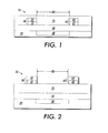
- FIGURE 1 represents a first embodiment of a TFT according to the present disclosure.
- FIGURE 2 represents a second embodiment of a TFT according to the present disclosure.
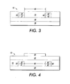
- FIGURE 3 represents a third embodiment of a TFT according to the present disclosure.
- FIGURE 4 represents a fourth embodiment of a TFT according to the present disclosure.
- Each source and drain electrode comprises a first layer including a first conductive material and a second layer including a second conductive material.
- the source electrode first layer may be the same as or different from the drain electrode first layer.
- the source electrode second layer may be the same as or different from the drain electrode second layer.
- References to the energy level of the semiconductor refer to the HOMO or LUMO level of the semiconductor depending on whether it is p-type or n-type semiconductor, respectively.
- FIGURE 1 illustrates a bottom-gate bottom-contact TFT configuration according to the present disclosure.
- the TFT 10 comprises a substrate 20 in contact with the gate electrode 30 and a gate dielectric layer 40.
- the gate electrode 30 is depicted within the substrate 20, this is not required.
- the gate dielectric layer 40 separates the gate electrode 30 from the source electrode 50, drain electrode 60, and the semiconductor layer 70.
- the source electrode 50 comprises a first layer 52 and a second layer 54.
- the drain electrode 60 also comprises a first layer 62 and a second layer 64.
- the first layer 62 is closer to the gate dielectric layer 40 than the second layer 64.
- the semiconductor layer 70 runs over and between the source and drain electrodes 50 and 60. Both layers 52, 54, 62, 64 of the source and drain electrodes 50 and 60 contact the semiconductor layer 70.
- the semiconductor has a channel length 80 between the source and drain electrodes 50 and 60.
- FIGURE 2 illustrates another bottom-gate top-contact TFT configuration according to the present disclosure.
- the TFT 10 comprises a substrate 20 in contact with the gate electrode 30 and a gate dielectric layer 40.
- the semiconductor layer 70 is placed on top of the gate dielectric layer 40 and separates it from the source and drain electrodes 50 and 60.
- the source electrode 50 comprises a first layer 52 and a second layer 54.
- the drain electrode 60 also comprises a first layer 62 and a second layer 64. Both layers 52, 54, 62, 64 of the source and drain electrodes 50 and 60 contact the semiconductor layer 70.
- FIGURE 3 illustrates a bottom-gate bottom-contact TFT configuration according to the present disclosure.
- the TFT 10 comprises a substrate 20 which also acts as the gate electrode and is in contact with a gate dielectric layer 40.
- the source electrode 50 comprises a first layer 52 and a second layer 54.
- the drain electrode 60 also comprises a first layer 62 and a second layer 64.
- the first layer 62 is closer to the gate dielectric layer 40 than the second layer 64.
- Both layers 52, 54, 62, 64 of the source and drain electrodes 50 and 60 contact the semiconductor layer 70.
- FIGURE 4 illustrates a top-gate top-contact TFT configuration according to the present disclosure.
- the TFT 10 comprises a substrate 20 in contact with the source electrode 50, drain electrode 60, and the semiconductor layer 70.
- the source electrode 50 comprises a first layer 52 and a second layer 54.
- the drain electrode 60 also comprises a first layer 62 and a second layer 64.
- the semiconductor layer 70 runs over and between the source and drain electrodes 50 and 60.
- the gate dielectric layer 40 is on top of the semiconductor layer 70.
- the gate electrode 30 is on top of the gate dielectric layer 40 and does not contact the semiconductor layer 70. Both layers 52, 54, 62, 64 of the source and drain electrodes 50 and 60 contact the semiconductor layer 70.
- the substrate may be composed of materials including but not limited to silicon, glass plate, plastic film or sheet.
- plastic substrate such as for example polyester, polycarbonate, polyimide sheets and the like may be preferred.
- the thickness of the substrate may be from about 10 micrometers to over 10 millimeters with an exemplary thickness being from about 50 to about 100 micrometers, especially for a flexible plastic substrate and from about 1 to about 10 millimeters for a rigid substrate such as glass or silicon.
- the gate electrode is composed of an electrically conductive material. It can be a thin metal film, a conducting polymer film, a conducting film made from conducting ink or paste, or the substrate itself, for example heavily doped silicon.
- Examples of gate electrode materials include but are not restricted to aluminum, gold, chromium, indium tin oxide, conductive polymers such as polystyrene sulfonate-doped poly(3,4-ethylenedioxythiophene) (PSS-PEDOT), and conducting ink/paste comprised of carbon black/graphite.
- the gate electrode can be prepared by vacuum evaporation, sputtering of metals or conductive metal oxides, conventional lithography and etching, chemical vapor deposition, spin coating, casting or printing, or other deposition processes.
- the thickness of the gate electrode ranges for example from about 10 to about 200 nanometers for metal films and from about 1 to about 10 micrometers for conductive polymers.
- the gate dielectric layer generally can be an inorganic material film or an organic polymer film.
- inorganic materials suitable as the gate dielectric layer include silicon oxide, silicon nitride, aluminum oxide, barium titanate, barium zirconium titanate and the like.
- suitable organic polymers include polyesters, polycarbonates, poly(vinyl phenol), polyimides, polystyrene, poly(methacrylate)s, poly(acrylate)s, epoxy resin and the like.
- the thickness of the gate dielectric layer depends on the dielectric constant of the material used and can be, for example, from about 5 nanometers to about 5000 nanometers, including from about 100 to about 1000 nanometers.
- the gate dielectric layer may have a conductivity that is, for example, less than about 10 -12 Siemens per centimeter (S/cm).
- the gate dielectric layer is formed using conventional processes known in the art, including those processes described in forming the gate electrode.
- the semiconductor layer generally is an organic semiconducting material.
- organic semiconductors include but are not limited to acenes, such as anthracene, tetracene, pentacene, and substituted pentacenes, perylenes, fullerenes, oligothiophenes, polythiophenes and their substituted derivatives, polypyrrole, poly-p-phenylenes, poly-p-phenylvinylidenes, naphthalenedicarboxylic dianhydrides, naphthalene-bisimides, polynaphthalenes, phthalocyanines such as copper phthalocyanines or zinc phthalocyanines and their substituted derivatives.
- the semiconductor may also be an inorganic semiconductor such as ZnO, ZnS, silicon nanowires, and the like.
- the semiconductors are polythiophenes.
- Polythiophenes include, for example, regioregular and regiorandom poly(3-alkylthiophene)s, polythiophenes comprising substituted and unsubstituted thienylene groups, polythiophenes comprising optionally substituted thieno[3,2-b]thiophene and/or optionally substituted thieno[2,3-b]thiophene groups, polythiophenes comprising fused-ring aromatic groups, polythiophenes comprising heteroatom-containing fused-ring aromatic groups, and polythiophenes comprising non-thiophene based aromatic groups such as phenylene, fluorene, furan, and the like.
- the semiconductor layer is from about 5 nanometers to about 1000 nanometers deep, including from about 20 to about 100 nanometers in depth. In certain configurations, such as the configurations shown in FIGURES 1 and 4 , the semiconductor layer completely covers the source and drain electrodes.
- the semiconductor layer has a channel length defined by the distance between the source and drain electrodes. In specific embodiments, the semiconductor channel length is at most 20 micrometers. In further embodiments, the semiconductor channel length is at most 10 micrometers. In specific embodiments, the semiconductor channel length is from about 5 to about 10 micrometers. In further embodiments, the semiconductor channel length is from about 1 to about 5 micrometers.
- the channel length is critical because a shorter channel length reduces R sc as discussed above. If R sc is large, then there is no need to introduce contact resistance to achieve a high current on/off ratio. In addition, a smaller channel length increase mobility.
- the semiconductor layer can be formed by molecular beam deposition, vacuum evaporation, sublimation, spin-on coating, dip coating, printing (e.g., inkjet printing, screen printing, stencil printing, microcontact printing, flexographic printing), and other conventional processes known in the art, including those processes described in forming the gate electrode.
- the organic semiconductor usually has a conductivity in the range of 10 -8 to 10 -4 S/cm. Various dopants known in the art may also be added to change the conductivity.
- the organic semiconductor can be either a p-type or n-type semiconductor.
- the semiconductor usually has an energy level (HOMO level) of higher than 4.5 eV.
- the p-type semiconductor has a HOMO level of about 5.1 eV.
- the semiconductor usually has a energy level (LUMO level) of lower than 4.5 eV.
- the n-type semiconductor has a LUMO level of about 4.0 eV.
- the semiconductor is a p-type semiconductor.
- the organic semiconductor is a polythiophene. Polythiophenes generally have a HOMO level of from about 4.7 eV to about 5.5 eV.
- the first layer of either the source or drain electrode has a work function differing from the energy level of the semiconductor layer by at least 0.5 eV.
- the work function of the first layer differs by 0.5 to about 1.0 eV.
- the difference is at least 1.0 eV.
- the second layer has a work function differing from the energy level of the semiconductor layer by at most 0.2 eV. In specific embodiments, the work function of the second layer differs from the energy level of the semiconductor layer by at most 0.1 eV.
- the second layer has a work function matching the energy level of the semiconductor layer. This difference is intentional because it introduces contact resistance into the TFT. It was surprisingly found that the combination of decreased R sc and increased R contact produced a TFT with both high mobility and high current on/off ratio.
- Metals suitable for use in the first layer of the source or drain electrode include, but are not limited to, platinum, gold, silver, nickel, chromium, copper, iron, tin, antimony, lead, tantalum, indium, palladium, tellurium, rhenium, iridium, aluminum, ruthenium, germanium, molybdenum, tungsten, tin oxide-antimony, indium tin oxide, fluorine-doped zinc oxide, zinc, carbon, graphite, glassy carbon, silver paste, carbon paste, lithium, beryllium, sodium, magnesium, potassium, calcium, scandium, titanium, manganese, zirconium, gallium, niobium, sodium, sodium-potassium alloy, magnesium, lithium, and their alloys.
- the cheaper conductive materials are used; they are silver, nickel, chromium, copper, iron, tin, antimony, lead, tantalum, indium, aluminum, tungsten, tin oxide-antimony, indium tin oxide, fluorine-doped zinc oxide, zinc, carbon, graphite, silver paste, and carbon paste. That the first layer must differ by at least 0.5 eV and the second layer must differ by at most 0.2 eV from the energy level of the semiconductor layer implies that the two electrode layers always comprise different materials.
- Conductive polymers may be used in the first layer of the source or drain electrode.
- Such conductive polymers include, but are not limited to, a polyaniline, polypyrrole, PSS-PEDOT, or their derivatives or their mixtures. These polymers may also be doped to enhance their conductivity. Generally, their conductivity is greater than 10 -3 S/cm.
- the first layer of either electrode should be no more than about 100 nanometers thick. In further embodiments, the first layer of either electrode has a thickness from about 5 nm to about 50 nm. In specific embodiments, the first layer of either electrode has a thickness at most 50 nm.
- the first layer can be formed by any deposition process known in the art, including those processes described in forming the gate electrode.
- the second layer can be from about 5 nanometers to about 3000 nanometers thick. In specific embodiments, the second layer has a thickness at least 20 nm, including from about 20 to about 1000 nanometers thick. The second layer can be formed by any deposition process known in the art, including those processes described in forming the gate electrode.
- a metal alloy may form at the interface between the first layer and the second layer of each electrode.
- the second metal layer is deposited after the first metal layer, there may be diffusion of the second layer metal into the first layer to form a metal alloy. This diffusion may take place in a range of about 0.1 nm to about 5 nm thickness.
- the first layers of both the source and drain electrodes are preferably composed of the same material, as are the second layers.
- the first layer of both the source and drain electrodes is titanium and the second layer of both electrodes is gold.
- Most p-type organic semiconductors have a work function of about 5.1 eV. Titanium has a work function of 4.1 eV, differing from the semiconductor by at least 0.5 eV.
- Gold has a work function of 5.1 eV as well, matching the semiconductor.
- the present disclosure also contemplates that the materials of both layers of either electrode are independently selected.
- both layers of the source and drain electrode directly contact the semiconductor layer.
- the source electrode first layer is closer to the gate dielectric layer than the source electrode second layer.
- the TFT is a bottom-gate bottom-contact TFT and the source electrode first layer directly contacts the gate dielectric layer.
- the TFT has dual-layer electrodes wherein the first layer of the source and drain electrodes have a work function differing from the energy level of the semiconductor layer by at least 0.5 eV.
- the second layers have a work function differing from the energy level of the semiconductor layer by at most 0.1 eV.
- the semiconductor channel length is at most 20 micrometers.
- both high mobility and high current on/off ratio are achieved.
- the various components of the OTFT may be deposited upon the substrate in any order.
- the gate electrode and the semiconductor layer should both be in contact with the gate dielectric layer.
- the source and drain electrodes should both be in contact with the semiconductor layer.
- both layers of the electrodes should be in contact with the semiconductor layer.
- a bottom-contact thin-film transistor with a configuration illustrated in Figure 3 was built. It comprised an n-doped silicon wafer with a thermally grown silicon oxide layer having a thickness of about 300 nanometers. The wafer functioned as the gate electrode. The silicon oxide layer functioned as the gate dielectric layer.
- a 10-nanometer layer of titanium was applied in two locations corresponding to the source and drain electrodes. This titanium layer was the first layer of the dual-layer electrodes. Next, a 100-nanometer layer of gold was applied to the titanium layers to form the second layer of the dual-layer electrodes.
- the semiconductor channel length i.e. distance between the source and drain electrodes
- the silicon oxide surface was modified with octyltrichlorosilane (OTS-8) by immersing the devices in 0.1 M OTS-8 solution in toluene at 60 °C for 20 min.
- OTS-8 octyltrichlorosilane
- the gold surface was then modified with octanethiol by immersing the devices in 0.01 M octanethiol solution in toluene at room temperature for 20 min.
- the following polythiophene was then deposited to form the semiconductor layer:
- n is a number of from about 5 to about 5,000.
- the polymer possessed an M w of 22,900 and M n of 17,300 relative to polystyrene standards.
- This polythiophene and its preparation are described in U.S. Patent No. 6,770,904 , the disclosure of which is totally incorporated herein by reference.
- the polythiophene was spin coated, then annealed at 140 °C (its phase transition temperature).
- the transistor had a semiconductor channel length of 5 microns and a channel width of 250 microns.
- the semiconductor had a HOMO level of 5.1 eV, which differed from the work function of the source electrode first titanium layer (4.1 eV) by 1.0 eV and matched the work function of the source electrode second gold layer (5.1 eV).
- the device was characterized using a Keithley 4200 SCS semiconductor characterization system.
- Another important property of a thin-film transistor is its current on/off ratio. This is the ratio of the saturation source-drain current when the gate voltage V G is equal to or greater than the drain voltage V D to the source-drain current when the gate voltage V G is zero.
- the mobility was calculated to be 0.39 cm 2 /V ⁇ sec and the current on/off ratio was about 10 7 .
- Comparative Example 1 a transistor was fabricated as in Example 1 except the source and drain electrodes were a single layer of gold and had a channel length of 90 microns. The mobility was calculated to be 0.12 cm 2 /V ⁇ sec and the current on/off ratio was about 10 7 .
- transistors were fabricated as in Example 1 except the source and drain electrodes were a single layer of gold and the channel length was 2 or 5 microns. They had mobility of up to 0.45 cm 2 /V ⁇ sec, but a current on/off ratio of less than 10 4 .
- Comparing Comparative Example 1 with Comparative Example 2 revealed that a short semiconductor channel length increased mobility significantly. Comparing Example 1 with Comparative Example 1 showed that without contact resistance, a short semiconductor channel length also dramatically decreased the current on/off ratio (from 10 7 to 10 4 ). By intentionally introducing contact resistance with the dual-layer electrode design, both high mobility and high current on/off ratio were achieved.
Landscapes
- Chemical & Material Sciences (AREA)
- Engineering & Computer Science (AREA)
- Materials Engineering (AREA)
- Inorganic Chemistry (AREA)
- Thin Film Transistor (AREA)
- Electroluminescent Light Sources (AREA)
- Electrodes Of Semiconductors (AREA)
Claims (15)
- Dünnschichttransistor (10), umfassend:eine Source-Elektrode (50); eine Drain-Elektrode (60); undeine Halbleiterschicht (70);wobei die Source-Elektrode (50) und die Drain-Elektrode (60) jeweils eine erste Schicht (52, 62) und eine zweite Schicht (54, 64) umfassen;wobei die erste Source-Elektrodenschicht (54) eine Austrittsarbeit aufweist, welche sich von dem Energieniveau der Halbleiterschicht (70) um wenigstens 0,5 eV unterscheidet;wobei die zweite Source-Elektrodenschicht (54) zwischen der ersten Schicht und der Halbleiterschicht angeordnet ist und eine Austrittsarbeit aufweist, welche sich von dem Energieniveau der Halbleiterschicht (70) um höchstens 0,2 eV unterscheidet;dadurch gekennzeichnet, dass die zweite Source-Elektrodenschicht (54) und die zweite Drain-Elektrodenschicht (64) unabhängig ein Material umfassen, gewählt aus der Gruppe bestehend aus Titan, Platin, Gold, Silber, Nickel, Chrom, Kupfer, Eisen, Zinn, Antimon, Blei, Tantal, Indium, Palladium, Tellur, Rhenium, Iridium, Aluminium, Ruthenium, Germanium, Molybdän, Wolfram, Zinnoxid-Antimon, Indiumzinnoxid, Fluor dotiertes Zinkoxid, Zink, Kohlenstoff, Graphit, Silberpaste, Karbonpaste, Lithium, Beryllium, Natrium, Magnesium, Kalium, Calcium, Scandium, Mangan, Zirkonium, Gallium, Niob, Natrium, Natriumkaliumlegierung, Magnesium, Lithium und deren Legierungen;wobei die Halbleiterschicht (70) eine Kanallänge von nicht mehr als 20 Mikrometer aufweist.
- Dünnschichttransistor (10) nach Anspruch 1, wobei die erste Source-Elektrodenschicht (52) und die erste Drain-Elektrodenschicht (62) unabhängig ein Material umfassen, gewählt aus der Gruppe bestehend aus Titan, Platin, Gold, Silber, Nickel, Chrom, Kupfer, Eisen, Zinn, Antimon, Blei, Tantal, Indium, Palladium, Tellur, Rhenium, Iridium, Aluminium, Ruthenium, Germanium, Molybdän, Wolfram, Antimon-Zinnoxid, Indiumzinnoxid, Fluor dotiertes Zinkoxid, Zink, Kohlenstoff, Graphit, Silberpaste, Karbonpaste, Lithium, Beryllium, Natrium, Magnesium, Kalium, Calcium, Scandium, Mangan, Zirkonium, Gallium, Niob, Natrium, Natriumkaliumlegierung, Magnesium, Lithium und deren Legierungen.
- Dünnschichttransistor (10) nach Anspruch 1 oder Anspruch 2, wobei die erste Source-Elektrodenschicht (52) und die erste Drain-Elektrodenschicht (62) jeweils eine Dicke von höchstens 50 Nanometer aufweisen.
- Dünnschichttransistor (10) nach einem der vorangehenden Ansprüche, wobei die zweite Source-Elektrodenschicht (54) und die zweite Drain-Elektrodenschicht (64) jeweils eine Dicke von wenigstens 5 Nanometer aufweisen.
- Dünnschichttransistor (10) nach einem der vorangehenden Ansprüche, wobei die zweite Source-Elektrodenschicht (54) und die zweite Drain-Elektrodenschicht (64) jeweils eine Dicke von ungefähr 20 bis ungefähr 1000 Nanometer aufweisen.
- Dünnschichttransistor (10) nach einem der vorangehenden Ansprüche, wobei der Unterschied zwischen dem Energieniveau der Halbleiterschicht (70) und der Austrittsarbeit der ersten Source-Elektrodenschicht (52) von 0,5 eV bis ungefähr 1,0 eV beträgt.
- Dünnschichttransistor (10) nach Anspruch 1 bis 5, wobei der Unterschied zwischen dem Energieniveau der Halbleiterschicht (70) und der Austrittsarbeit der ersten Source-Elektrodenschicht (52) wenigstens 1,0 eV beträgt.
- Dünnschichttransistor (10) nach einem der vorangehenden Ansprüche, wobei die Halbleiterschicht (70) eine Kanallänge von ungefähr 5 bis ungefähr 10 Mikrometer aufweist.
- Dünnschichttransistor (10) nach einem der vorangehenden Ansprüche, wobei die erste Source-Elektrodenschicht (52), die erste Drain-Elektrodenschicht (62), die zweite Source-Elektrodenschicht (54) und die zweite Drain-Elektrodenschicht (64) jeweils direkt die Halbleiterschicht (70) kontaktieren.
- Dünnschichttransistor (10) nach einem der vorangehenden Ansprüche, wobei die zweite Source-Elektrodenschicht (54) eine Austrittsarbeit aufweist, welche dem Energieniveau der Halbleiterschicht (70) entspricht.
- Dünnschichttransistor (10) nach Anspruch 1, wobei der Dünnschichttransistor (10) ein organischer Dünnschichttransistor ist und wobei die Halbleiterschicht (70) eine organische Halbleiterschicht ist;
wobei jede erste Schicht (52, 62) eine Austrittsarbeit aufweist, welche sich von dem Energieniveau der Halbleiterschicht (70) um wenigstens 0,5 eV unterscheidet;
wobei jede zweite Schicht (54, 64) eine Austrittsarbeit aufweist, welche sich von dem Energieniveau der Halbleiterschicht (70) um höchstens 0,2 eV unterscheidet; und
wobei die Halbleiterschicht (70) eine Kanallänge von ungefähr 5 bis ungefähr 10 Mikrometer aufweist. - Dünnschichttransistor (10) nach Anspruch 11, wobei die erste Source-Elektrodenschicht (52) der dielektrischen Gate-Schicht (40) näher ist als die zweite Source-Elektrodenschicht (54).
- Dünnschichttransistor nach Anspruch 11 oder Anspruch 12, wobei der Unterschied der Austrittsarbeit zwischen der Halbleiterschicht (70) und jeder ersten Schicht (54, 64) von 0,5 eV bis ungefähr 1,0 eV beträgt.
- Dünnschichttransistor (10) nach einem der Ansprüche 11 und 12, wobei der Unterschied der Austrittsarbeit zwischen der organischen Halbleiterschicht und jeder ersten Schicht (52, 62) wenigstens 1,0 eV beträgt.
- Dünnschichttransistor (10) nach Anspruch 1, wobei der Dünnschichttransistor ein organischer Dünnschichttransistor ist, in welchem die Halbleiterschicht (70) eine Polythiophen-Halbleiterschicht ist;
wobei die Source-Elektrode (50) und die Drain-Elektrode (60) jeweils eine erste Schicht aus Titan und eine zweite Schicht aus Gold umfassen; und
wobei die Halbleiterschicht (70) eine Kanallänge von höchstens ungefähr 10 Mikrometer aufweist.
Applications Claiming Priority (1)
| Application Number | Priority Date | Filing Date | Title |
|---|---|---|---|
| US11/564,438 US7923718B2 (en) | 2006-11-29 | 2006-11-29 | Organic thin film transistor with dual layer electrodes |
Publications (3)
| Publication Number | Publication Date |
|---|---|
| EP1928038A2 EP1928038A2 (de) | 2008-06-04 |
| EP1928038A3 EP1928038A3 (de) | 2009-07-01 |
| EP1928038B1 true EP1928038B1 (de) | 2013-05-29 |
Family
ID=38947399
Family Applications (1)
| Application Number | Title | Priority Date | Filing Date |
|---|---|---|---|
| EP07121765.7A Active EP1928038B1 (de) | 2006-11-29 | 2007-11-28 | Organischer Dünnfilmtransistor mit Doppelschichtelektroden |
Country Status (7)
| Country | Link |
|---|---|
| US (1) | US7923718B2 (de) |
| EP (1) | EP1928038B1 (de) |
| JP (1) | JP2008141197A (de) |
| KR (1) | KR101474934B1 (de) |
| CN (1) | CN101192623A (de) |
| CA (1) | CA2612033C (de) |
| TW (1) | TW200835010A (de) |
Families Citing this family (17)
| Publication number | Priority date | Publication date | Assignee | Title |
|---|---|---|---|---|
| JP2010040897A (ja) * | 2008-08-07 | 2010-02-18 | Sony Corp | 有機薄膜トランジスタ、有機薄膜トランジスタの製造方法、および電子機器 |
| US20100032654A1 (en) * | 2008-08-11 | 2010-02-11 | Motorola, Inc. | Semiconductor Device Having Silane Treated Interface |
| JP5501604B2 (ja) * | 2008-12-04 | 2014-05-28 | シャープ株式会社 | 有機薄膜トランジスタ |
| GB2467357B (en) * | 2009-01-30 | 2011-09-21 | Cambridge Display Tech Ltd | Organic thin film transistors |
| WO2011145814A2 (ko) * | 2010-05-19 | 2011-11-24 | 경희대학교 산학협력단 | 박막 트랜지스터 및 그 제조 방법 |
| KR101839329B1 (ko) | 2011-07-28 | 2018-03-19 | 엘지디스플레이 주식회사 | 트랜지스터 어레이 기판 및 그의 제조방법 |
| KR101934978B1 (ko) * | 2011-08-04 | 2019-01-04 | 삼성디스플레이 주식회사 | 박막 트랜지스터 및 박막 트랜지스터 표시판 |
| GB201114215D0 (en) * | 2011-08-18 | 2011-10-05 | Cambridge Display Tech Ltd | Electronic device |
| US20140251407A1 (en) * | 2011-09-28 | 2014-09-11 | Fujifilm Corporation | Thermoelectric conversion material and a thermoelectric conversion element |
| US20160141530A1 (en) * | 2013-06-11 | 2016-05-19 | Sharp Kabushiki Kaisha | Semiconductor element and semiconductor element manufacturing method |
| JP5557304B1 (ja) * | 2013-09-26 | 2014-07-23 | 国立大学法人東北大学 | 有機半導体素子及びそれを備えたcmis半導体装置 |
| GB2521138B (en) * | 2013-12-10 | 2019-01-02 | Flexenable Ltd | Source/Drain Conductors for Transistor Devices |
| JP6452126B2 (ja) * | 2014-09-18 | 2019-01-16 | 国立研究開発法人物質・材料研究機構 | 有機半導体トランジスタ及びその製造方法 |
| CN105185835A (zh) * | 2015-07-30 | 2015-12-23 | 京东方科技集团股份有限公司 | 一种薄膜晶体管及其制作方法、阵列基板、显示装置 |
| GB2561246A (en) * | 2017-04-07 | 2018-10-10 | Sumitomo Chemical Co | Gas Sensor system and method |
| CN113506831A (zh) * | 2021-06-21 | 2021-10-15 | 武汉大学 | 一种短沟道ZnO薄膜晶体管及其制备方法 |
| US12615804B1 (en) | 2024-10-31 | 2026-04-28 | Zinite Corporation | Thin-film transistors with metal oxide channel interfaces |
Family Cites Families (26)
| Publication number | Priority date | Publication date | Assignee | Title |
|---|---|---|---|---|
| JP3403949B2 (ja) * | 1998-09-03 | 2003-05-06 | シャープ株式会社 | 薄膜トランジスタ及び液晶表示装置、ならびに薄膜トランジスタの製造方法 |
| US6910933B1 (en) * | 1999-10-05 | 2005-06-28 | Matsushita Electric Industrial Co., Ltd. | Light emitting element and producing method thereof, and display device and lighting device using the same |
| US6953947B2 (en) | 1999-12-31 | 2005-10-11 | Lg Chem, Ltd. | Organic thin film transistor |
| TWI286773B (en) * | 2000-10-26 | 2007-09-11 | Matsushita Electric Works Ltd | Field emission type electron source |
| GB2373095A (en) * | 2001-03-09 | 2002-09-11 | Seiko Epson Corp | Patterning substrates with evaporation residues |
| KR100379684B1 (ko) * | 2001-04-20 | 2003-04-10 | 엘지.필립스 엘시디 주식회사 | 박막 트랜지스터 액정표시소자 제조방법 |
| JP4360801B2 (ja) * | 2001-12-25 | 2009-11-11 | シャープ株式会社 | トランジスタおよびそれを用いた表示装置 |
| US6770904B2 (en) | 2002-01-11 | 2004-08-03 | Xerox Corporation | Polythiophenes and electronic devices generated therefrom |
| US7250625B2 (en) * | 2002-01-11 | 2007-07-31 | Xerox Corporation | Polythiophenes and electronic devices generated therefrom |
| EP1383179A2 (de) * | 2002-07-17 | 2004-01-21 | Pioneer Corporation | Organische Halbleiteranordnung |
| JP2004055654A (ja) * | 2002-07-17 | 2004-02-19 | Pioneer Electronic Corp | 有機半導体素子 |
| JP2004055876A (ja) * | 2002-07-22 | 2004-02-19 | Renesas Technology Corp | 半導体装置及び半導体装置の製造方法 |
| JP2004103905A (ja) | 2002-09-11 | 2004-04-02 | Pioneer Electronic Corp | 有機半導体素子 |
| US7102155B2 (en) * | 2003-09-04 | 2006-09-05 | Hitachi, Ltd. | Electrode substrate, thin film transistor, display device and their production |
| JP4550389B2 (ja) * | 2003-09-12 | 2010-09-22 | 株式会社日立製作所 | 半導体装置 |
| JP4353842B2 (ja) * | 2004-03-31 | 2009-10-28 | 三洋電機株式会社 | 有機薄膜トランジスタの製造方法 |
| JP4774679B2 (ja) | 2004-03-31 | 2011-09-14 | 大日本印刷株式会社 | 有機半導体装置 |
| JP4826074B2 (ja) * | 2004-08-18 | 2011-11-30 | ソニー株式会社 | 電界効果型トランジスタ |
| KR100659061B1 (ko) * | 2004-09-20 | 2006-12-19 | 삼성에스디아이 주식회사 | 유기 박막 트랜지스터 및 이를 구비한 평판표시장치 |
| US7355199B2 (en) * | 2004-11-02 | 2008-04-08 | E.I. Du Pont De Nemours And Company | Substituted anthracenes and electronic devices containing the substituted anthracenes |
| JP4341529B2 (ja) * | 2004-11-05 | 2009-10-07 | セイコーエプソン株式会社 | 電子デバイス、電子デバイスの製造方法および電子機器 |
| CN101057347B (zh) * | 2004-11-09 | 2013-02-20 | 创造者科技有限公司 | 制造有机晶体管的自动对准方法 |
| US7719496B2 (en) * | 2004-11-23 | 2010-05-18 | Samsung Mobile Display Co., Ltd. | Organic thin film transistor, method of manufacturing the same, and flat panel display device with the organic thin film transistor |
| US7262264B2 (en) * | 2005-01-12 | 2007-08-28 | Honeywell International Inc. | Halogenated thiophene monomer for the preparation of regioregular polythiophenes |
| US20060273303A1 (en) | 2005-06-07 | 2006-12-07 | Xerox Corporation. | Organic thin film transistors with multilayer electrodes |
| JP2007200829A (ja) * | 2005-12-27 | 2007-08-09 | Semiconductor Energy Lab Co Ltd | 有機発光トランジスタ |
-
2006
- 2006-11-29 US US11/564,438 patent/US7923718B2/en active Active
-
2007
- 2007-11-22 CA CA2612033A patent/CA2612033C/en not_active Expired - Fee Related
- 2007-11-26 JP JP2007304164A patent/JP2008141197A/ja active Pending
- 2007-11-28 KR KR1020070122019A patent/KR101474934B1/ko active Active
- 2007-11-28 EP EP07121765.7A patent/EP1928038B1/de active Active
- 2007-11-28 CN CNA2007101961472A patent/CN101192623A/zh active Pending
- 2007-11-28 TW TW096145066A patent/TW200835010A/zh unknown
Non-Patent Citations (1)
| Title |
|---|
| STEPHEN R FORREST: "The Limits to Organic Photovoltaic Cell Efficiency", MRS BULLETIN, vol. 30, 1 January 2005 (2005-01-01), pages 28 - 32, XP055050619 * |
Also Published As
| Publication number | Publication date |
|---|---|
| JP2008141197A (ja) | 2008-06-19 |
| EP1928038A3 (de) | 2009-07-01 |
| KR20080048960A (ko) | 2008-06-03 |
| CA2612033A1 (en) | 2008-05-29 |
| US20080121869A1 (en) | 2008-05-29 |
| TW200835010A (en) | 2008-08-16 |
| EP1928038A2 (de) | 2008-06-04 |
| KR101474934B1 (ko) | 2014-12-19 |
| CA2612033C (en) | 2013-09-10 |
| US7923718B2 (en) | 2011-04-12 |
| CN101192623A (zh) | 2008-06-04 |
Similar Documents
| Publication | Publication Date | Title |
|---|---|---|
| CA2612033C (en) | Organic thin film transistor with dual layer electrodes | |
| EP1732150A1 (de) | Organischer Dünnfilmtransistor mit mehrlagigen Elektroden | |
| US7863600B2 (en) | Field-effect transistor | |
| US8293363B2 (en) | Thin-film transistors | |
| US7795611B2 (en) | Field effect organic transistor | |
| US7875878B2 (en) | Thin film transistors | |
| EP2117059B1 (de) | Organische Dünnschichttransistoren | |
| US8952359B2 (en) | Electronic device and method of manufacturing the same, and semiconductor device and method of manufacturing the same | |
| EP2157114A1 (de) | Halbleitende Polymere | |
| US20100090201A1 (en) | Organic thin film transistors | |
| EP2157119A1 (de) | Elektronisches Gerät, das halbleitende Polymere umfasst | |
| US8729222B2 (en) | Organic thin-film transistors | |
| EP1675195A2 (de) | Organischer Dünnfilmtransistor für eine OLED Anzeigevorrichtung | |
| JP5014567B2 (ja) | 基体上の誘電体層とその作製方法 | |
| US7573063B1 (en) | Organic thin film transistors | |
| US8134144B2 (en) | Thin-film transistor |
Legal Events
| Date | Code | Title | Description |
|---|---|---|---|
| PUAI | Public reference made under article 153(3) epc to a published international application that has entered the european phase |
Free format text: ORIGINAL CODE: 0009012 |
|
| AK | Designated contracting states |
Kind code of ref document: A2 Designated state(s): AT BE BG CH CY CZ DE DK EE ES FI FR GB GR HU IE IS IT LI LT LU LV MC MT NL PL PT RO SE SI SK TR |
|
| AX | Request for extension of the european patent |
Extension state: AL BA HR MK RS |
|
| PUAL | Search report despatched |
Free format text: ORIGINAL CODE: 0009013 |
|
| AK | Designated contracting states |
Kind code of ref document: A3 Designated state(s): AT BE BG CH CY CZ DE DK EE ES FI FR GB GR HU IE IS IT LI LT LU LV MC MT NL PL PT RO SE SI SK TR |
|
| AX | Request for extension of the european patent |
Extension state: AL BA HR MK RS |
|
| 17P | Request for examination filed |
Effective date: 20100104 |
|
| AKX | Designation fees paid |
Designated state(s): DE FR GB |
|
| 17Q | First examination report despatched |
Effective date: 20100218 |
|
| GRAP | Despatch of communication of intention to grant a patent |
Free format text: ORIGINAL CODE: EPIDOSNIGR1 |
|
| GRAS | Grant fee paid |
Free format text: ORIGINAL CODE: EPIDOSNIGR3 |
|
| GRAA | (expected) grant |
Free format text: ORIGINAL CODE: 0009210 |
|
| AK | Designated contracting states |
Kind code of ref document: B1 Designated state(s): DE FR GB |
|
| REG | Reference to a national code |
Ref country code: GB Ref legal event code: FG4D |
|
| REG | Reference to a national code |
Ref country code: DE Ref legal event code: R096 Ref document number: 602007030738 Country of ref document: DE Effective date: 20130725 |
|
| REG | Reference to a national code |
Ref country code: DE Ref legal event code: R081 Ref document number: 602007030738 Country of ref document: DE Owner name: SAMSUNG ELECTRONICS CO., LTD., KR Free format text: FORMER OWNER: XEROX CORPORATION, ROCHESTER, US Effective date: 20130820 Ref country code: DE Ref legal event code: R081 Ref document number: 602007030738 Country of ref document: DE Owner name: SAMSUNG ELECTRONICS CO., LTD., SUWON-SI, KR Free format text: FORMER OWNER: XEROX CORPORATION, ROCHESTER, N.Y., US Effective date: 20130820 |
|
| REG | Reference to a national code |
Ref country code: FR Ref legal event code: TP Owner name: SAMSUNG ELECTRONICS CO., LTD., KR Effective date: 20131105 |
|
| REG | Reference to a national code |
Ref country code: GB Ref legal event code: 732E Free format text: REGISTERED BETWEEN 20140306 AND 20140312 |
|
| PLBE | No opposition filed within time limit |
Free format text: ORIGINAL CODE: 0009261 |
|
| STAA | Information on the status of an ep patent application or granted ep patent |
Free format text: STATUS: NO OPPOSITION FILED WITHIN TIME LIMIT |
|
| 26N | No opposition filed |
Effective date: 20140303 |
|
| REG | Reference to a national code |
Ref country code: DE Ref legal event code: R097 Ref document number: 602007030738 Country of ref document: DE Effective date: 20140303 |
|
| REG | Reference to a national code |
Ref country code: FR Ref legal event code: PLFP Year of fee payment: 10 |
|
| REG | Reference to a national code |
Ref country code: FR Ref legal event code: PLFP Year of fee payment: 11 |
|
| REG | Reference to a national code |
Ref country code: FR Ref legal event code: PLFP Year of fee payment: 12 |
|
| REG | Reference to a national code |
Ref country code: DE Ref legal event code: R079 Ref document number: 602007030738 Country of ref document: DE Free format text: PREVIOUS MAIN CLASS: H01L0051100000 Ipc: H10K0010800000 |
|
| PGFP | Annual fee paid to national office [announced via postgrant information from national office to epo] |
Ref country code: DE Payment date: 20251022 Year of fee payment: 19 |
|
| PGFP | Annual fee paid to national office [announced via postgrant information from national office to epo] |
Ref country code: GB Payment date: 20251016 Year of fee payment: 19 |
|
| PGFP | Annual fee paid to national office [announced via postgrant information from national office to epo] |
Ref country code: FR Payment date: 20251023 Year of fee payment: 19 |