EP1928086B1 - Procédés et appareil de gain simultané automatique, phase et correction de décalage cc dans des récepteurs de communication - Google Patents
Procédés et appareil de gain simultané automatique, phase et correction de décalage cc dans des récepteurs de communication Download PDFInfo
- Publication number
- EP1928086B1 EP1928086B1 EP07113614A EP07113614A EP1928086B1 EP 1928086 B1 EP1928086 B1 EP 1928086B1 EP 07113614 A EP07113614 A EP 07113614A EP 07113614 A EP07113614 A EP 07113614A EP 1928086 B1 EP1928086 B1 EP 1928086B1
- Authority
- EP
- European Patent Office
- Prior art keywords
- digital value
- channel
- digital
- equal
- output
- Prior art date
- Legal status (The legal status is an assumption and is not a legal conclusion. Google has not performed a legal analysis and makes no representation as to the accuracy of the status listed.)
- Not-in-force
Links
Images

Classifications
-
- H—ELECTRICITY
- H04—ELECTRIC COMMUNICATION TECHNIQUE
- H04L—TRANSMISSION OF DIGITAL INFORMATION, e.g. TELEGRAPHIC COMMUNICATION
- H04L27/00—Modulated-carrier systems
- H04L27/32—Carrier systems characterised by combinations of two or more of the types covered by groups H04L27/02, H04L27/10, H04L27/18 or H04L27/26
- H04L27/34—Amplitude- and phase-modulated carrier systems, e.g. quadrature-amplitude modulated carrier systems
- H04L27/38—Demodulator circuits; Receiver circuits
- H04L27/3809—Amplitude regulation arrangements
-
- H—ELECTRICITY
- H03—ELECTRONIC CIRCUITRY
- H03D—DEMODULATION OR TRANSFERENCE OF MODULATION FROM ONE CARRIER TO ANOTHER
- H03D3/00—Demodulation of angle-, frequency- or phase- modulated oscillations
- H03D3/007—Demodulation of angle-, frequency- or phase- modulated oscillations by converting the oscillations into two quadrature related signals
- H03D3/008—Compensating DC offsets
-
- H—ELECTRICITY
- H03—ELECTRONIC CIRCUITRY
- H03D—DEMODULATION OR TRANSFERENCE OF MODULATION FROM ONE CARRIER TO ANOTHER
- H03D3/00—Demodulation of angle-, frequency- or phase- modulated oscillations
- H03D3/007—Demodulation of angle-, frequency- or phase- modulated oscillations by converting the oscillations into two quadrature related signals
- H03D3/009—Compensating quadrature phase or amplitude imbalances
-
- H—ELECTRICITY
- H04—ELECTRIC COMMUNICATION TECHNIQUE
- H04L—TRANSMISSION OF DIGITAL INFORMATION, e.g. TELEGRAPHIC COMMUNICATION
- H04L25/00—Baseband systems
- H04L25/02—Details ; arrangements for supplying electrical power along data transmission lines
- H04L25/06—DC level restoring means; Bias distortion correction ; Decision circuits providing symbol by symbol detection
- H04L25/061—DC level restoring means; Bias distortion correction ; Decision circuits providing symbol by symbol detection providing hard decisions only; arrangements for tracking or suppressing unwanted low frequency components, e.g. removal of DC offset
- H04L25/063—Setting decision thresholds using feedback techniques only
-
- H—ELECTRICITY
- H04—ELECTRIC COMMUNICATION TECHNIQUE
- H04L—TRANSMISSION OF DIGITAL INFORMATION, e.g. TELEGRAPHIC COMMUNICATION
- H04L27/00—Modulated-carrier systems
- H04L27/32—Carrier systems characterised by combinations of two or more of the types covered by groups H04L27/02, H04L27/10, H04L27/18 or H04L27/26
- H04L27/34—Amplitude- and phase-modulated carrier systems, e.g. quadrature-amplitude modulated carrier systems
- H04L27/38—Demodulator circuits; Receiver circuits
- H04L27/3845—Demodulator circuits; Receiver circuits using non - coherent demodulation, i.e. not using a phase synchronous carrier
- H04L27/3854—Demodulator circuits; Receiver circuits using non - coherent demodulation, i.e. not using a phase synchronous carrier using a non - coherent carrier, including systems with baseband correction for phase or frequency offset
- H04L27/3863—Compensation for quadrature error in the received signal
-
- H—ELECTRICITY
- H04—ELECTRIC COMMUNICATION TECHNIQUE
- H04L—TRANSMISSION OF DIGITAL INFORMATION, e.g. TELEGRAPHIC COMMUNICATION
- H04L27/00—Modulated-carrier systems
- H04L27/0014—Carrier regulation
- H04L2027/0044—Control loops for carrier regulation
- H04L2027/0053—Closed loops
- H04L2027/0057—Closed loops quadrature phase
-
- H—ELECTRICITY
- H04—ELECTRIC COMMUNICATION TECHNIQUE
- H04L—TRANSMISSION OF DIGITAL INFORMATION, e.g. TELEGRAPHIC COMMUNICATION
- H04L27/00—Modulated-carrier systems
- H04L27/0014—Carrier regulation
Definitions
- the invention relates to a method of DC offset correction in a communication receiver according to the preamble of claim 1. Accordingly, the present invention relates to the field of communication receivers.
- a method of DC offset correction in a communication receiver of the above-mentioned type is known, for example, from WO 00/51254 A .
- An exemplary receiver in which the preferred embodiments of the present invention may be used may have a low noise amplifier coupled to an antenna, a mixer and filter followed by a variable gain amplifier (VGA) and then an analog to digital converter (ADC).
- VGA variable gain amplifier
- ADC analog to digital converter
- the "mixer” may be two mixers providing I and Q channel outputs, each mixer being followed by a filter and VGA. It is assumed for purposes of this disclosure that each VGA is digitally controlled, though that is not a limitation of the invention.
- the ADC is a 2 bit converter having possible outputs of 00, 01, 10 and 11, though this is not a limitation of the invention.
- the minimum and maximum outputs shall be referred to as the extreme outputs.
- the present invention is not limited to use with such converters, and may be used with N bit converters where N is any value of two or more.
- Gain control is required in modern wireless receivers due to the large variations in signal amplitude caused by unpredictable over-the-air channels. Additional gain variation is caused by intra-receiver component variations, causing a decrease in sensitivity unless corrected.
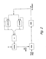
- the gain control loop for a given channel operates by counting the number of extreme codes at the output of the ADC in a given time period. At the end of this time period, the number of extreme codes is compared (COMP) to a predefined reference level or count (Gain Ref), obtained a-priori by studying the expected signal statistics. If the number of counts exceeds the reference level, the output gain code is decreased to decrease the gain of the VGA. In the preferred embodiment, the gain code is decreased by some number proportional to the excess number of counts. If the count falls short, the gain code is increased, again by an appropriately scaled version of the count-to-reference difference.
- the necessary accumulation time and gain control step size can be determined to ensure a given level of gain error. The technique works even when the source signal is dominated by channel noise, since these statistics are also knowable.
- the gain control loop provides the input of the ADC with a constant-power signal that optimally fills the converter, even under adverse communication conditions.
- the gain control scheme described above can also be used to correct gain imbalances arising from component mismatches between the I and Q paths.
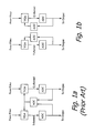
- One known method of gain control in I & Q receivers shown in Figure 1a provides the same gain voltage or code to both the I and Q sections, relying on analog circuit matching to ensure a match in I and Q channel gain.
- the above gain control technique is used independently in both channels as shown in Figure 1b , its self-correcting nature will in fact correct die-to-die analog circuit variations.
- the mismatch will be a uniformly distributed statistical parameter shown in Figure 1d , with the limits of the distribution being no greater than the minimum step size of the VGA used. For typical 6 ⁇ process limits, this leads to a significant improvement in gain mismatch.
- the I and Q channels will exhibit the same power over an appropriate accumulation time.
- Each channel's gain control loop will converge to the same value, and thus the long-term gain error will always be smaller than the minimum gain step size.
- the VGA and ADC circuits exhibit non-zero DC offsets due to parameter mismatches.
- the large baseband gains typically present in the receiver cause these DC offsets to reduce maximum signal handling capability, hence a DC offset correction scheme is necessary.
- the DC offset correction loop of the present invention operates by again counting the number of extreme codes at the output of the ADC as defined in claim 1.
- the registers used in the gain control loop are reused for this purpose.
- the difference between the upper extreme code count and the lower extreme code count over a predefined period of time is, assuming a zero-mean input signal, proportional to the DC offset created by the analog VGA.
- the difference is positive, the DC offset correction must bring the DC offset down.
- the difference is negative, the DC offset correction must bring the DC offset up. This is done in the compensation circuit Comp.
- Two such loops are used in a receiver having I and Q channels. The two loops may operate simultaneously, or alternatively one after the other.
- the DC offset correction is independent of gain control. This is because the two operations which provide the error signal in the two loops (a sum in the case of the gain control loop, a subtraction in the case of the DC control loop) are orthogonal to each other, hence cannot affect each other. In the case of large perturbations of the converged state, the operation of the two loops can be made independent by separating their time constants.
- the accumulation time can easily be increased or decreased to capture the true statistics of the input. In the preferred embodiment, this can be done by modifying the counter length, but the invention is not limited to this method.
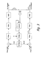
- a phase imbalance correction circuit is illustrated in Figure 3 .
- I t A t ⁇ sin ⁇ t + B t ⁇ cos ⁇ t ⁇ sin ⁇ t
- Q t A t ⁇ sin ⁇ t + B t ⁇ cos ⁇ t ⁇ cos ⁇ t + ⁇
- the second term is simply the cross-correlation of the two bitstreams A(t) B(t), which must be zero since they are uncorrelated.
- the technique is insensitive to gain imbalances between I and Q channels though not, as will be shown, to DC offsets in each.
- phase error cancellation technique is, to a first order, insensitive to DC offsets.
- phase-correction system operates very well with uncorrelated I and Q signals, such as Gaussian noise.
- correlation is present, a different technique can be used.
- a pilot tone is used to train the receiver before receiving data and the present invention is active only during the pilot tone.
- a sinusoid of random phase will have orthogonal components in I and Q, so the relevant integral again reduces to zero.
- the above-described set of control loops can elegantly be implemented in digital logic, taking as their input the output bits of the ADC, and providing as their output a set of digital words that control the analog blocks to close the loops.
- the gain control loop is implemented as a pair of accumulators which count the number of extreme codes in a given time period. At the end of this time period, the sum of the two accumulators is subtracted from a reference bit word. If the difference exceeds some positive threshold, a scaled version of the difference is subtracted from the output gain word. If the difference is smaller than some negative threshold, again a scaled version of the difference is added to the output gain word. In this way, it is possible to control both the gain and hysteresis of the gain loop.
- a limiter is also used in order to avoid causing overflow and underflow of the gain word.
- the DC offset loop takes the same accumulators as the gain control loop but subtracts them. If this number exceeds some positive hysteresis threshold, a scaled version of the difference is subtracted from the output DC offset correction word. Similarly, if the difference is lower than some negative threshold, a scaled version of the difference is added to the output word. This scheme again provides control of the DC loop gain and hysteresis.
- the phase imbalance correction loop is implemented with a digital multiplier that multiplies the I channel and Q channel ADC outputs. This value is accumulated in a large register for a given time period. At the end of this time period, the value of the accumulator represents, the positive half-cycle.
- the input to the Q channel VGA is then inverted using switches, and the output of the I channel ADC is logically inverted.
- the input to the I channel VGA could be inverted using switches, and the output of the Q channel ADC could be logically inverted before the multiplication.
- the signal that is inverted before the respective VGA should be reinverted at the output of the phase imbalance correction block, or in further signal processing circuitry not shown.
- the same accumulation is performed for the same time period.
- the value of the accumulator is proportional to the phase imbalance. If this imbalance exceeds some threshold, a scaled version of the accumulator is used to adjust the I/Q balance in the LO or mixer.
- the method Since a typical implementation is largely digital, there are significant savings in power, and the method has an easily programmable tradeoff between accuracy and speed. By eliminating the need for analog power detectors, phase detectors, and DC servo loops, the method also decreases the precision analog content of the receiver, thereby reducing complexity and increasing robustness against implementation inaccuracies. This leads to lower die area, improved yields, and a reduced off-chip component count.
- the method can operate on received data directly. Thus, in most cases, there is no need for a training sequence or other calibration periods that prevent the receiver from being used to receive useful data.
- the present invention is not limited to use with 2 bit converters, and may be used with N bit converters where N is any value of two or more.
- N any value of two or more.
- a code may be considered extreme if it approaches either limit by some predetermined magnitude, such as by way of example, one half or three quarters of its extreme value.
- different predetermined magnitudes might be used for different compensation loops.
- one may use the same accumulator values for the gain compensation (the sum of the values) as for DC offset compensation (the difference in the values).
- the time constants may be separated by controlling the amount the gain and DC offset are adjusted in a given correction period, as controlling the loop-gain of a correction loop controls its time constant.
- these two loops are intentionally given much different integration times so that they operate independently during startup or in the presence of a large signal disturbance.
- the DC offset compensation loop is not sensitive to signal statistics or on orthogonality or signal independence between channels, so may continue to operate after the training time for signals that are not independent or perfectly orthogonal. Otherwise implementation and operation of the invention can remain as described. Whether N is 2 or is more than 2, the accumulators effectively operate as counters.
Landscapes
- Engineering & Computer Science (AREA)
- Power Engineering (AREA)
- Computer Networks & Wireless Communication (AREA)
- Signal Processing (AREA)
- Analogue/Digital Conversion (AREA)
- Control Of Amplification And Gain Control (AREA)
- Circuits Of Receivers In General (AREA)
- Superheterodyne Receivers (AREA)
- Digital Transmission Methods That Use Modulated Carrier Waves (AREA)
Claims (16)
- Procédé de correction de décalage CC dans un récepteur de communication ayant des canaux I et Q, chaque canal ayant un amplificateur ayant une sortie couplée à un convertisseur analogique-numérique, ADC, délivrant des sorties numériques s'échelonnant d'une valeur numérique la plus faible à une valeur numérique la plus élevée, caractérisé en ce qu'il comprend les étapes consistant à :accumuler, pour chaque canal, pendant une première période de temps, un premier décompte du nombre de sorties de l'ADC égal ou supérieur à une deuxième valeur numérique supérieure et accumuler un deuxième décompte du nombre de sorties numériques égal ou inférieur à une deuxième valeur numérique inférieure, la grandeur d'une différence quelconque entre la deuxième valeur numérique supérieure et une valeur numérique la plus élevée étant la même que la grandeur d'une différence quelconque entre la deuxième valeur numérique inférieure et une valeur numérique la plus faible,réduire, si le premier décompte est supérieur au deuxième décompte pour un canal, le décalage d'entrée pour le canal respectif ; etaugmenter, si le premier décompte est inférieur au deuxième décompte pour un canal, le décalage d'entrée pour le canal respectif.
- Procédé selon la revendication 1, dans lequel le décalage CC est modifié d'une quantité sensible à la différence entre le premier et le deuxième décompte et le gain de l'amplificateur du canal respectif est modifié d'une quantité sensible à la somme des premier et deuxième décomptes.
- Procédé selon la revendication 1, dans lequel la sortie numérique est une sortie numérique de deux bits et la deuxième valeur numérique supérieure est égale à la valeur numérique la plus élevée et la deuxième valeur numérique inférieure est égale à la valeur numérique la plus faible.
- Procédé selon la revendication 1, comprenant une correction de gain dans le récepteur de communication, dans lequel chaque canal a un amplificateur de gain variable, VGA, et comprenant en outre les étapes consistant à :accumuler, pour chaque canal, pendant une deuxième période de temps, un troisième décompte du nombre de sorties de l'ADC égal ou supérieur à une troisième valeur numérique supérieure et accumuler un quatrième décompte du nombre de sorties numériques qui est égal ou inférieur à une troisième valeur numérique inférieure, la grandeur d'une différence quelconque entre la troisième valeur numérique supérieure et la valeur numérique la plus élevée étant identique à la grandeur d'une différence quelconque entre la troisième valeur numérique inférieure et la valeur numérique la plus faible,augmenter, si le total des troisième et quatrième décomptes pour un canal est inférieur à un nombre prédéterminé, le gain du VGA dans le canal respectif ; etréduire, si le total des troisième et quatrième décomptes pour un ou plusieurs canaux est supérieur à un nombre prédéterminé, le gain du VGA dans le canal respectif.
- Procédé selon la revendication 4, dans lequel les première et deuxième périodes de temps sont des périodes de temps différentes.
- Procédé selon la revendication 5, dans lequel les première et deuxième périodes de temps sont des périodes de temps de durée différente.
- Procédé selon la revendication 4, dans lequel les première et deuxième périodes de temps sont des périodes de temps de durée différente.
- Procédé selon la revendication 4, dans lequel le décalage CC est modifié d'une quantité sensible à la différence entre les premier et deuxième décomptes et le gain est modifié d'une quantité sensible à la somme des troisième et quatrième décomptes.
- Procédé selon la revendication 4, dans lequel la deuxième valeur numérique supérieure est égale à la troisième valeur numérique supérieure et la deuxième valeur numérique inférieure est égale à la troisième valeur numérique inférieure.
- Procédé selon la revendication 4, dans lequel la sortie numérique est une sortie numérique de deux bits, et les troisième et deuxième valeurs numériques supérieures sont égales à la valeur numérique la plus élevée et les troisième et deuxièmes valeurs numériques inférieures sont égales à la valeur numérique la plus faible.
- Procédé selon la revendication 1, comprenant une correction de phase dans le récepteur de communication, comprenant en outre les étapes consistant à :accumuler, pendant la moitié d'une deuxième période de temps, le produit de la sortie de l'ADC dans le canal I et de la sortie de l'ADC dans le canal Q et, pendant l'autre moitié de la deuxième période de temps, accumuler le produit de l'inverse de la sortie de l'ADC d'un canal et de l'inverse de l'entrée du VGA de l'autre canal ; etajuster la phase entre les canaux I et Q sensibles aux accumulations combinées pendant les deux moitiés de la deuxième période de temps pour réduire l'erreur de phase.
- Procédé selon la revendication 11, dans lequel la sortie numérique est une sortie numérique de deux bits et la deuxième valeur numérique supérieure est égale à la valeur numérique la plus élevée et la deuxième valeur numérique inférieure est égale à la valeur numérique la plus faible.
- Procédé selon la revendication 1, comprenant une correction de gain et de phase dans un récepteur de communication, comprenant en outre les étapes consistant à :accumuler, pour chaque canal, pendant une deuxième période de temps, un troisième décompte du nombre de sorties de l'ADC égal ou supérieur à une troisième valeur numérique supérieure et accumuler un quatrième décompte du nombre de sorties numériques égal ou inférieur à une troisième valeur numérique inférieure, la grandeur d'une différence quelconque entre la troisième valeur numérique supérieure et la valeur numérique la plus élevée étant identique à la grandeur d'une différence quelconque entre la troisième valeur numérique inférieure et la valeur numérique la plus faible,augmenter, si le total des troisième et quatrième décomptes pour un canal est inférieur à un nombre prédéterminé, le gain du VGA dans le canal respectif ;réduire, si le total des troisième et quatrième décomptes pour un ou plusieurs canaux est supérieur à un nombre prédéterminé, le gain du VGA dans le canal respectif ;accumuler, pendant la moitié de la deuxième période de temps, le produit de la sortie de l'ADC dans le canal I et de la sortie de l'ADC dans le canal Q et, pendant l'autre moitié de la deuxième période de temps, accumuler le produit de l'inverse de la sortie de l'ADC d'un canal et l'inverse de l'entrée du VGA de l'autre canal ; etajuster la phase entre les canaux I et Q sensibles aux accumulations combinées pendant les deux moitiés de la deuxième période de temps pour réduire l'erreur de phase.
- Procédé selon la revendication 13, dans lequel la phase est ajustée en quantité proportionnelle à la somme des produits accumulés.
- Procédé selon la revendication 14, dans lequel la phase est ajustée en quantité proportionnelle à la somme des produits accumulés si les produits accumulés dépassent un seuil prédéterminé.
- Procédé selon la revendication 15, dans lequel la sortie numérique est une sortie numérique de deux bits et les troisième et deuxième valeurs numériques supérieures sont égales à la valeur numérique la plus élevée et les troisième et deuxièmes valeurs numériques inférieures sont égales à la valeur numérique la plus faible.
Applications Claiming Priority (1)
| Application Number | Priority Date | Filing Date | Title |
|---|---|---|---|
| US11/605,617 US7769116B2 (en) | 2006-11-28 | 2006-11-28 | Methods and apparatus for simultaneous automatic gain, phase and DC offset correction in communication receivers |
Publications (3)
| Publication Number | Publication Date |
|---|---|
| EP1928086A2 EP1928086A2 (fr) | 2008-06-04 |
| EP1928086A3 EP1928086A3 (fr) | 2009-06-24 |
| EP1928086B1 true EP1928086B1 (fr) | 2010-11-17 |
Family
ID=39218355
Family Applications (1)
| Application Number | Title | Priority Date | Filing Date |
|---|---|---|---|
| EP07113614A Not-in-force EP1928086B1 (fr) | 2006-11-28 | 2007-08-01 | Procédés et appareil de gain simultané automatique, phase et correction de décalage cc dans des récepteurs de communication |
Country Status (4)
| Country | Link |
|---|---|
| US (1) | US7769116B2 (fr) |
| EP (1) | EP1928086B1 (fr) |
| AT (1) | ATE488908T1 (fr) |
| DE (1) | DE602007010571D1 (fr) |
Families Citing this family (4)
| Publication number | Priority date | Publication date | Assignee | Title |
|---|---|---|---|---|
| US8792590B2 (en) * | 2009-02-25 | 2014-07-29 | Harris Corporation | Communications device with in-phase/quadrature (I/Q) DC offset, gain and phase imbalance compensation and related method |
| JP4809450B2 (ja) * | 2009-02-26 | 2011-11-09 | パナソニック株式会社 | デルタシグマad変調器 |
| CN105610760B (zh) * | 2016-01-29 | 2018-11-16 | 深圳市极致汇仪科技有限公司 | 无线综测仪对单载波qpsk信号iq不平衡的检测方法 |
| US10594281B1 (en) | 2019-03-04 | 2020-03-17 | Ciena Corporation | Receiver automatic gain control systems and methods for asymmetrical or unbalanced constellations |
Family Cites Families (9)
| Publication number | Priority date | Publication date | Assignee | Title |
|---|---|---|---|---|
| US4540974A (en) * | 1981-10-30 | 1985-09-10 | Rca Corporation | Adaptive analog-to-digital converter |
| JP2574441B2 (ja) * | 1987-03-20 | 1997-01-22 | 富士通株式会社 | ディジタル復調装置 |
| US5761251A (en) * | 1995-11-08 | 1998-06-02 | Philips Electronics North America Corporation | Dual automatic gain control and DC offset correction circuit for QAM demodulation |
| US6757340B1 (en) | 1999-02-22 | 2004-06-29 | Telefonaktiebolaget L M Ericsson (Publ) | Radio receiver and method for preloading an average DC-offset into a channel filter |
| DE19933266A1 (de) | 1999-07-15 | 2000-11-02 | Siemens Ag | Vorrichtung zum Empfangen von Funksignalen |
| US6901121B1 (en) * | 2001-02-20 | 2005-05-31 | Comsys Communication & Signal Processing Ltd. | Compensation of DC offset impairment in a communications receiver |
| US6941121B2 (en) * | 2001-05-18 | 2005-09-06 | Rf Micro Devices, Inc. | Method for calibrating a DC offset cancellation level for direct conversion receivers |
| US7310387B2 (en) * | 2003-12-26 | 2007-12-18 | Electronics And Telecommunications Research Institute | Apparatus for compensating DC offsets, gain and phase imbalances between I-channel and Q-channel in quadrature transceiving system |
| US7620373B2 (en) * | 2006-06-23 | 2009-11-17 | Sierra Monolithics, Inc. | Apparatus and method for calibration of gain and/or phase imbalance and/or DC offset in a communication system |
-
2006
- 2006-11-28 US US11/605,617 patent/US7769116B2/en active Active
-
2007
- 2007-08-01 EP EP07113614A patent/EP1928086B1/fr not_active Not-in-force
- 2007-08-01 AT AT07113614T patent/ATE488908T1/de not_active IP Right Cessation
- 2007-08-01 DE DE602007010571T patent/DE602007010571D1/de active Active
Also Published As
| Publication number | Publication date |
|---|---|
| ATE488908T1 (de) | 2010-12-15 |
| DE602007010571D1 (de) | 2010-12-30 |
| EP1928086A2 (fr) | 2008-06-04 |
| US7769116B2 (en) | 2010-08-03 |
| US20080123785A1 (en) | 2008-05-29 |
| EP1928086A3 (fr) | 2009-06-24 |
Similar Documents
| Publication | Publication Date | Title |
|---|---|---|
| US7589657B2 (en) | Analog to digital converter with interference rejection capability | |
| EP1303910B1 (fr) | Circuit de commande de gain automatique | |
| US6417730B1 (en) | Automatic gain control system and related method | |
| KR100474085B1 (ko) | 디씨 오프셋 보상 회로 및 방법과 이를 이용한 신호 처리장치 | |
| US7003271B2 (en) | Direct conversion receiver having a gain-setting dependent filter parameter | |
| US20050276358A1 (en) | Wireless LAN receiver with I and Q RF and baseband AGC loops and DC offset cancellation | |
| US7929650B2 (en) | AGC for narrowband receivers | |
| EP1928086B1 (fr) | Procédés et appareil de gain simultané automatique, phase et correction de décalage cc dans des récepteurs de communication | |
| EP3235128A1 (fr) | Récepteur radio en mode paquet avec commande de gain automatique | |
| KR20050006209A (ko) | 트랜스시버 디바이스에 대한 디지털 자동 이득 제어 | |
| US7373125B2 (en) | Off-channel signal detector with programmable hysteresis | |
| US6686861B1 (en) | Slice circuit capable of accurate conversion of an analog signal to a digital signal | |
| US7277510B1 (en) | Adaptation algorithm based on signal statistics for automatic gain control | |
| US9444661B2 (en) | DC offset tracking of wireless receivers | |
| CN100420150C (zh) | 用于高增益信号信道的偏置量校准系统和方法 | |
| US8497733B2 (en) | Offset correction circuit | |
| US8223900B2 (en) | Receiver with mixed-mode automatic gain control | |
| US20060178125A1 (en) | Receiver for wireless communication systems and I/O signal phase difference correction method therefor | |
| US7643803B2 (en) | Power estimation of a transmission | |
| US7145490B2 (en) | Automatic gain control system and method | |
| EP1884016B1 (fr) | Procede et systeme de correction de desequilibre i/q et de decalage en cc | |
| SE520193C2 (sv) | Anordning och förfarande för förstärkningsstyrning | |
| US20070047670A1 (en) | High-frequency detection mechanism and automatic gain control system utilizing the same | |
| JP2009524321A (ja) | Dcオフセットを減少させる方法 | |
| WO2011065142A1 (fr) | Dispositif de réception et procédé de commande du gain |
Legal Events
| Date | Code | Title | Description |
|---|---|---|---|
| PUAI | Public reference made under article 153(3) epc to a published international application that has entered the european phase |
Free format text: ORIGINAL CODE: 0009012 |
|
| AK | Designated contracting states |
Kind code of ref document: A2 Designated state(s): AT BE BG CH CY CZ DE DK EE ES FI FR GB GR HU IE IS IT LI LT LU LV MC MT NL PL PT RO SE SI SK TR |
|
| AX | Request for extension of the european patent |
Extension state: AL BA HR MK RS |
|
| PUAL | Search report despatched |
Free format text: ORIGINAL CODE: 0009013 |
|
| AK | Designated contracting states |
Kind code of ref document: A3 Designated state(s): AT BE BG CH CY CZ DE DK EE ES FI FR GB GR HU IE IS IT LI LT LU LV MC MT NL PL PT RO SE SI SK TR |
|
| AX | Request for extension of the european patent |
Extension state: AL BA HR MK RS |
|
| 17P | Request for examination filed |
Effective date: 20091228 |
|
| AKX | Designation fees paid |
Designated state(s): AT BE BG CH CY CZ DE DK EE ES FI FR GB GR HU IE IS IT LI LT LU LV MC MT NL PL PT RO SE SI SK TR |
|
| GRAP | Despatch of communication of intention to grant a patent |
Free format text: ORIGINAL CODE: EPIDOSNIGR1 |
|
| GRAS | Grant fee paid |
Free format text: ORIGINAL CODE: EPIDOSNIGR3 |
|
| GRAA | (expected) grant |
Free format text: ORIGINAL CODE: 0009210 |
|
| AK | Designated contracting states |
Kind code of ref document: B1 Designated state(s): AT BE BG CH CY CZ DE DK EE ES FI FR GB GR HU IE IS IT LI LT LU LV MC MT NL PL PT RO SE SI SK TR |
|
| REG | Reference to a national code |
Ref country code: GB Ref legal event code: FG4D |
|
| REG | Reference to a national code |
Ref country code: CH Ref legal event code: EP |
|
| REG | Reference to a national code |
Ref country code: IE Ref legal event code: FG4D |
|
| REF | Corresponds to: |
Ref document number: 602007010571 Country of ref document: DE Date of ref document: 20101230 Kind code of ref document: P |
|
| REG | Reference to a national code |
Ref country code: NL Ref legal event code: VDEP Effective date: 20101117 |
|
| LTIE | Lt: invalidation of european patent or patent extension |
Effective date: 20101117 |
|
| PG25 | Lapsed in a contracting state [announced via postgrant information from national office to epo] |
Ref country code: LT Free format text: LAPSE BECAUSE OF FAILURE TO SUBMIT A TRANSLATION OF THE DESCRIPTION OR TO PAY THE FEE WITHIN THE PRESCRIBED TIME-LIMIT Effective date: 20101117 |
|
| PG25 | Lapsed in a contracting state [announced via postgrant information from national office to epo] |
Ref country code: CY Free format text: LAPSE BECAUSE OF FAILURE TO SUBMIT A TRANSLATION OF THE DESCRIPTION OR TO PAY THE FEE WITHIN THE PRESCRIBED TIME-LIMIT Effective date: 20101117 Ref country code: SE Free format text: LAPSE BECAUSE OF FAILURE TO SUBMIT A TRANSLATION OF THE DESCRIPTION OR TO PAY THE FEE WITHIN THE PRESCRIBED TIME-LIMIT Effective date: 20101117 Ref country code: FI Free format text: LAPSE BECAUSE OF FAILURE TO SUBMIT A TRANSLATION OF THE DESCRIPTION OR TO PAY THE FEE WITHIN THE PRESCRIBED TIME-LIMIT Effective date: 20101117 Ref country code: AT Free format text: LAPSE BECAUSE OF FAILURE TO SUBMIT A TRANSLATION OF THE DESCRIPTION OR TO PAY THE FEE WITHIN THE PRESCRIBED TIME-LIMIT Effective date: 20101117 Ref country code: LV Free format text: LAPSE BECAUSE OF FAILURE TO SUBMIT A TRANSLATION OF THE DESCRIPTION OR TO PAY THE FEE WITHIN THE PRESCRIBED TIME-LIMIT Effective date: 20101117 Ref country code: NL Free format text: LAPSE BECAUSE OF FAILURE TO SUBMIT A TRANSLATION OF THE DESCRIPTION OR TO PAY THE FEE WITHIN THE PRESCRIBED TIME-LIMIT Effective date: 20101117 Ref country code: IS Free format text: LAPSE BECAUSE OF FAILURE TO SUBMIT A TRANSLATION OF THE DESCRIPTION OR TO PAY THE FEE WITHIN THE PRESCRIBED TIME-LIMIT Effective date: 20110317 Ref country code: SI Free format text: LAPSE BECAUSE OF FAILURE TO SUBMIT A TRANSLATION OF THE DESCRIPTION OR TO PAY THE FEE WITHIN THE PRESCRIBED TIME-LIMIT Effective date: 20101117 Ref country code: PT Free format text: LAPSE BECAUSE OF FAILURE TO SUBMIT A TRANSLATION OF THE DESCRIPTION OR TO PAY THE FEE WITHIN THE PRESCRIBED TIME-LIMIT Effective date: 20110317 Ref country code: BG Free format text: LAPSE BECAUSE OF FAILURE TO SUBMIT A TRANSLATION OF THE DESCRIPTION OR TO PAY THE FEE WITHIN THE PRESCRIBED TIME-LIMIT Effective date: 20110217 |
|
| PG25 | Lapsed in a contracting state [announced via postgrant information from national office to epo] |
Ref country code: GR Free format text: LAPSE BECAUSE OF FAILURE TO SUBMIT A TRANSLATION OF THE DESCRIPTION OR TO PAY THE FEE WITHIN THE PRESCRIBED TIME-LIMIT Effective date: 20110218 |
|
| PG25 | Lapsed in a contracting state [announced via postgrant information from national office to epo] |
Ref country code: BE Free format text: LAPSE BECAUSE OF FAILURE TO SUBMIT A TRANSLATION OF THE DESCRIPTION OR TO PAY THE FEE WITHIN THE PRESCRIBED TIME-LIMIT Effective date: 20101117 Ref country code: CZ Free format text: LAPSE BECAUSE OF FAILURE TO SUBMIT A TRANSLATION OF THE DESCRIPTION OR TO PAY THE FEE WITHIN THE PRESCRIBED TIME-LIMIT Effective date: 20101117 Ref country code: EE Free format text: LAPSE BECAUSE OF FAILURE TO SUBMIT A TRANSLATION OF THE DESCRIPTION OR TO PAY THE FEE WITHIN THE PRESCRIBED TIME-LIMIT Effective date: 20101117 Ref country code: ES Free format text: LAPSE BECAUSE OF FAILURE TO SUBMIT A TRANSLATION OF THE DESCRIPTION OR TO PAY THE FEE WITHIN THE PRESCRIBED TIME-LIMIT Effective date: 20110228 |
|
| PG25 | Lapsed in a contracting state [announced via postgrant information from national office to epo] |
Ref country code: PL Free format text: LAPSE BECAUSE OF FAILURE TO SUBMIT A TRANSLATION OF THE DESCRIPTION OR TO PAY THE FEE WITHIN THE PRESCRIBED TIME-LIMIT Effective date: 20101117 Ref country code: RO Free format text: LAPSE BECAUSE OF FAILURE TO SUBMIT A TRANSLATION OF THE DESCRIPTION OR TO PAY THE FEE WITHIN THE PRESCRIBED TIME-LIMIT Effective date: 20101117 Ref country code: SK Free format text: LAPSE BECAUSE OF FAILURE TO SUBMIT A TRANSLATION OF THE DESCRIPTION OR TO PAY THE FEE WITHIN THE PRESCRIBED TIME-LIMIT Effective date: 20101117 Ref country code: DK Free format text: LAPSE BECAUSE OF FAILURE TO SUBMIT A TRANSLATION OF THE DESCRIPTION OR TO PAY THE FEE WITHIN THE PRESCRIBED TIME-LIMIT Effective date: 20101117 |
|
| PLBE | No opposition filed within time limit |
Free format text: ORIGINAL CODE: 0009261 |
|
| STAA | Information on the status of an ep patent application or granted ep patent |
Free format text: STATUS: NO OPPOSITION FILED WITHIN TIME LIMIT |
|
| 26N | No opposition filed |
Effective date: 20110818 |
|
| REG | Reference to a national code |
Ref country code: DE Ref legal event code: R097 Ref document number: 602007010571 Country of ref document: DE Effective date: 20110818 |
|
| PG25 | Lapsed in a contracting state [announced via postgrant information from national office to epo] |
Ref country code: MT Free format text: LAPSE BECAUSE OF FAILURE TO SUBMIT A TRANSLATION OF THE DESCRIPTION OR TO PAY THE FEE WITHIN THE PRESCRIBED TIME-LIMIT Effective date: 20101117 Ref country code: IT Free format text: LAPSE BECAUSE OF FAILURE TO SUBMIT A TRANSLATION OF THE DESCRIPTION OR TO PAY THE FEE WITHIN THE PRESCRIBED TIME-LIMIT Effective date: 20101117 |
|
| PG25 | Lapsed in a contracting state [announced via postgrant information from national office to epo] |
Ref country code: MC Free format text: LAPSE BECAUSE OF NON-PAYMENT OF DUE FEES Effective date: 20110831 |
|
| REG | Reference to a national code |
Ref country code: CH Ref legal event code: PL |
|
| GBPC | Gb: european patent ceased through non-payment of renewal fee |
Effective date: 20110801 |
|
| PG25 | Lapsed in a contracting state [announced via postgrant information from national office to epo] |
Ref country code: CH Free format text: LAPSE BECAUSE OF NON-PAYMENT OF DUE FEES Effective date: 20110831 Ref country code: LI Free format text: LAPSE BECAUSE OF NON-PAYMENT OF DUE FEES Effective date: 20110831 |
|
| REG | Reference to a national code |
Ref country code: FR Ref legal event code: ST Effective date: 20120430 |
|
| REG | Reference to a national code |
Ref country code: IE Ref legal event code: MM4A |
|
| PG25 | Lapsed in a contracting state [announced via postgrant information from national office to epo] |
Ref country code: IE Free format text: LAPSE BECAUSE OF NON-PAYMENT OF DUE FEES Effective date: 20110801 |
|
| PG25 | Lapsed in a contracting state [announced via postgrant information from national office to epo] |
Ref country code: FR Free format text: LAPSE BECAUSE OF NON-PAYMENT OF DUE FEES Effective date: 20110831 Ref country code: GB Free format text: LAPSE BECAUSE OF NON-PAYMENT OF DUE FEES Effective date: 20110801 |
|
| REG | Reference to a national code |
Ref country code: DE Ref legal event code: R082 Ref document number: 602007010571 Country of ref document: DE Representative=s name: CANZLER & BERGMEIER PATENTANWAELTE, DE |
|
| REG | Reference to a national code |
Ref country code: DE Ref legal event code: R081 Ref document number: 602007010571 Country of ref document: DE Owner name: MAXIM INTEGRATED PRODUCTS, INC., US Free format text: FORMER OWNER: MAXIM INTEGRATED PRODUCTS, INC., SUNNYVALE, US Effective date: 20121203 Ref country code: DE Ref legal event code: R081 Ref document number: 602007010571 Country of ref document: DE Owner name: MAXIM INTEGRATED PRODUCTS, INC., SAN JOSE, US Free format text: FORMER OWNER: MAXIM INTEGRATED PRODUCTS, INC., SUNNYVALE, CALIF., US Effective date: 20121203 Ref country code: DE Ref legal event code: R082 Ref document number: 602007010571 Country of ref document: DE Representative=s name: CANZLER & BERGMEIER PATENTANWAELTE, DE Effective date: 20121203 Ref country code: DE Ref legal event code: R082 Ref document number: 602007010571 Country of ref document: DE Representative=s name: PATENTANWAELTE CANZLER & BERGMEIER PARTNERSCHA, DE Effective date: 20121203 |
|
| PG25 | Lapsed in a contracting state [announced via postgrant information from national office to epo] |
Ref country code: LU Free format text: LAPSE BECAUSE OF NON-PAYMENT OF DUE FEES Effective date: 20110801 |
|
| PG25 | Lapsed in a contracting state [announced via postgrant information from national office to epo] |
Ref country code: TR Free format text: LAPSE BECAUSE OF FAILURE TO SUBMIT A TRANSLATION OF THE DESCRIPTION OR TO PAY THE FEE WITHIN THE PRESCRIBED TIME-LIMIT Effective date: 20101117 |
|
| PG25 | Lapsed in a contracting state [announced via postgrant information from national office to epo] |
Ref country code: HU Free format text: LAPSE BECAUSE OF FAILURE TO SUBMIT A TRANSLATION OF THE DESCRIPTION OR TO PAY THE FEE WITHIN THE PRESCRIBED TIME-LIMIT Effective date: 20101117 |
|
| PGFP | Annual fee paid to national office [announced via postgrant information from national office to epo] |
Ref country code: DE Payment date: 20240723 Year of fee payment: 18 |
|
| REG | Reference to a national code |
Ref country code: DE Ref legal event code: R119 Ref document number: 602007010571 Country of ref document: DE |