EP1930867A2 - Affichage à plasma et son procédé de commande - Google Patents
Affichage à plasma et son procédé de commande Download PDFInfo
- Publication number
- EP1930867A2 EP1930867A2 EP07121004A EP07121004A EP1930867A2 EP 1930867 A2 EP1930867 A2 EP 1930867A2 EP 07121004 A EP07121004 A EP 07121004A EP 07121004 A EP07121004 A EP 07121004A EP 1930867 A2 EP1930867 A2 EP 1930867A2
- Authority
- EP
- European Patent Office
- Prior art keywords
- voltage
- transistor
- inductor
- electrodes
- coupled
- Prior art date
- Legal status (The legal status is an assumption and is not a legal conclusion. Google has not performed a legal analysis and makes no representation as to the accuracy of the status listed.)
- Withdrawn
Links
Images




Classifications
-
- G—PHYSICS
- G09—EDUCATION; CRYPTOGRAPHY; DISPLAY; ADVERTISING; SEALS
- G09G—ARRANGEMENTS OR CIRCUITS FOR CONTROL OF INDICATING DEVICES USING STATIC MEANS TO PRESENT VARIABLE INFORMATION
- G09G3/00—Control arrangements or circuits, of interest only in connection with visual indicators other than cathode-ray tubes
- G09G3/20—Control arrangements or circuits, of interest only in connection with visual indicators other than cathode-ray tubes for presentation of an assembly of a number of characters, e.g. a page, by composing the assembly by combination of individual elements arranged in a matrix no fixed position being assigned to or needed to be assigned to the individual characters or partial characters
- G09G3/22—Control arrangements or circuits, of interest only in connection with visual indicators other than cathode-ray tubes for presentation of an assembly of a number of characters, e.g. a page, by composing the assembly by combination of individual elements arranged in a matrix no fixed position being assigned to or needed to be assigned to the individual characters or partial characters using controlled light sources
- G09G3/28—Control arrangements or circuits, of interest only in connection with visual indicators other than cathode-ray tubes for presentation of an assembly of a number of characters, e.g. a page, by composing the assembly by combination of individual elements arranged in a matrix no fixed position being assigned to or needed to be assigned to the individual characters or partial characters using controlled light sources using luminous gas-discharge panels, e.g. plasma panels
- G09G3/288—Control arrangements or circuits, of interest only in connection with visual indicators other than cathode-ray tubes for presentation of an assembly of a number of characters, e.g. a page, by composing the assembly by combination of individual elements arranged in a matrix no fixed position being assigned to or needed to be assigned to the individual characters or partial characters using controlled light sources using luminous gas-discharge panels, e.g. plasma panels using AC panels
- G09G3/296—Driving circuits for producing the waveforms applied to the driving electrodes
-
- G—PHYSICS
- G09—EDUCATION; CRYPTOGRAPHY; DISPLAY; ADVERTISING; SEALS
- G09G—ARRANGEMENTS OR CIRCUITS FOR CONTROL OF INDICATING DEVICES USING STATIC MEANS TO PRESENT VARIABLE INFORMATION
- G09G3/00—Control arrangements or circuits, of interest only in connection with visual indicators other than cathode-ray tubes
- G09G3/20—Control arrangements or circuits, of interest only in connection with visual indicators other than cathode-ray tubes for presentation of an assembly of a number of characters, e.g. a page, by composing the assembly by combination of individual elements arranged in a matrix no fixed position being assigned to or needed to be assigned to the individual characters or partial characters
- G09G3/22—Control arrangements or circuits, of interest only in connection with visual indicators other than cathode-ray tubes for presentation of an assembly of a number of characters, e.g. a page, by composing the assembly by combination of individual elements arranged in a matrix no fixed position being assigned to or needed to be assigned to the individual characters or partial characters using controlled light sources
- G09G3/28—Control arrangements or circuits, of interest only in connection with visual indicators other than cathode-ray tubes for presentation of an assembly of a number of characters, e.g. a page, by composing the assembly by combination of individual elements arranged in a matrix no fixed position being assigned to or needed to be assigned to the individual characters or partial characters using controlled light sources using luminous gas-discharge panels, e.g. plasma panels
- G09G3/288—Control arrangements or circuits, of interest only in connection with visual indicators other than cathode-ray tubes for presentation of an assembly of a number of characters, e.g. a page, by composing the assembly by combination of individual elements arranged in a matrix no fixed position being assigned to or needed to be assigned to the individual characters or partial characters using controlled light sources using luminous gas-discharge panels, e.g. plasma panels using AC panels
- G09G3/296—Driving circuits for producing the waveforms applied to the driving electrodes
- G09G3/2965—Driving circuits for producing the waveforms applied to the driving electrodes using inductors for energy recovery
-
- G—PHYSICS
- G09—EDUCATION; CRYPTOGRAPHY; DISPLAY; ADVERTISING; SEALS
- G09G—ARRANGEMENTS OR CIRCUITS FOR CONTROL OF INDICATING DEVICES USING STATIC MEANS TO PRESENT VARIABLE INFORMATION
- G09G2330/00—Aspects of power supply; Aspects of display protection and defect management
- G09G2330/04—Display protection
- G09G2330/045—Protection against panel overheating
-
- G—PHYSICS
- G09—EDUCATION; CRYPTOGRAPHY; DISPLAY; ADVERTISING; SEALS
- G09G—ARRANGEMENTS OR CIRCUITS FOR CONTROL OF INDICATING DEVICES USING STATIC MEANS TO PRESENT VARIABLE INFORMATION
- G09G2330/00—Aspects of power supply; Aspects of display protection and defect management
- G09G2330/06—Handling electromagnetic interferences [EMI], covering emitted as well as received electromagnetic radiation
Definitions
- aspects of the present invention relate to a plasma display device and a driving method thereof.
- a plasma display device is a display device having a plasma display panel (hereafter, referred to as "PDP") for displaying text or an image, using plasma generated by a gas discharge.
- the PDP includes a plurality of driving circuit portions that are driven to produce a moving picture.
- the PDP of the plasma display device is driven by dividing one frame into a plurality of sub-fields that each have a weight value. Each sub-field is divided into a reset period, an address period, and a sustain period. Light emitting cells and non-light emitting cells are selected during the address periods, and a sustain discharge is applied to the addressed light emitting cells, so as to actually display an image, during the sustain periods. Further, a gray level is displayed, according to a combination of the weight values of the sub-fields.
- Electrodes to which the sustain pulses are applied during the sustain periods, are operated under a capacitive load.
- a reactive power is provided for a charge injection, in addition to providing a non-reactive power for a sustain discharge.
- An energy recovery circuit that recovers and reuses the reactive power is used in the sustain discharge circuit.
- the energy recovery circuit may use an inductor to boost an input voltage up to a high voltage for use in a sustain pulse.
- the voltage is stored in the inductor during a falling period of the sustain pulse, when the voltage of the sustain pulse is decreasing.
- the voltage stored in the inductor is reduced to a ground voltage, through a transistor coupled to a ground terminal. Accordingly, the transistor coupled with the ground terminal performs a hard switching, as the inductor is charged during the falling period of the sustain pulse.
- the energy recovery rate has been increased, in order to reduce the amount of reactive power used, by increasing the voltage stored in the inductor, and by increasing the amount of hard switching performed by the transistor coupled to the ground terminal. Accordingly, the power consumption and heat stress of the transistor is increased, thereby frequently causing the transistor to malfunction and electromagnetic interference (EMI) to occur.
- EMI electromagnetic interference
- aspects of the present invention provide a plasma display device and a driving method thereof, which can minimize the hard switching of a transistor.
- a plasma display device which includes: an inductor coupled to a plurality of first electrodes; a first transistor coupled between a contact of the plurality of first electrodes and the inductor, and a first power supply to supply a first voltage; a second transistor coupled between a contact of the plurality of first electrodes and the inductor, and a second power supply to supply a second voltage that is lower than the first voltage; a third transistor coupled between a third power supply, to supply a third voltage, and the inductor; a fourth transistor coupled in parallel with the third transistor; and a discharge part coupled between the second power supply and the plurality of first electrodes, to form a discharge path for discharging a voltage stored in the inductor.
- the discharge part may further include a fifth transistor, coupled to the plurality of first electrodes, to control the flow of the voltage stored in the inductor; a capacitor coupled between the fifth transistor and the second power supply; and a resistor coupled in parallel with the capacitor.
- the fifth transistor may be turned on before the second transistor is turned on.
- a voltage of the first electrode is increased when the third transistor is turned on.
- the first voltage is applied to the first electrode when the first transistor is turned on.
- a voltage of the first electrode is decreased when the fourth transistor is turned on.
- a voltage stored in the inductor is discharged when the fifth transistor is turned on.
- the second voltage is applied to the first electrode when the second transistor is turned on.
- the third power supply may further include a capacitor having an anode coupled to a contact of the third and fourth transistors.
- the third power supply may further include a first diode, coupled between the inductor and the third transistor, to control the direction of a current, so as to increase the voltage of the first electrode.
- the third power supply can include a second diode, coupled between the inductor and the fourth transistor, to control the direction of a current, so as to decrease the voltage of the first electrode.
- the second voltage may be a ground voltage.
- a driving method of a plasma display device which includes: increasing a voltage of the plurality of first electrodes using an inductor; applying a first voltage of a first power supply to the plurality of first electrodes; reducing the voltage of the plurality of first electrodes using the inductor; discharging a voltage stored in the inductor, using a discharge part, coupled between a second power supply to supply a second voltage that is lower than the first voltage, and the plurality of first electrodes; and applying the second voltage to the plurality of first electrodes.
- the operation of discharging the voltage stored in the inductor may include: turning on a transistor coupled between contacts of the inductor and the plurality of first electrodes; charging a capacitor using a voltage stored in the inductor that was supplied through the transistor; and consuming the voltage stored in the capacitor through a discharge resistor.
- FIG. 1 is a block diagram illustrating a plasma display device 100, according to aspects of the present invention.
- the plasma display device includes: a plasma display panel (PDP) 106 to display an image; an address driver 104 to supply data to a plurality of address electrodes (A1 to Am) of the PDP 106; a scan driver 102 to drive a plurality of scan electrodes (Y1 to Yn) (or first electrodes), a sustain driver 108 to drive a plurality of sustain electrodes (X1 to Xn), and a controller 110 to control the drivers 102, 104, and 108.
- PDP plasma display panel
- A1 to Am address electrodes
- Y1 to Yn scan electrodes
- a sustain driver 108 to drive a plurality of sustain electrodes (X1 to Xn)
- controller 110 to control the drivers 102, 104, and 108.
- the PDP 106 displays an image using a plurality of discharging cells (C) arranged in the form of a matrix.
- the PDP 106 includes the plurality of address electrodes (A1 to Am), which extend in a column direction, the plurality of scan electrodes (Y1 to Yn), which extend in a row direction, and the plurality of sustain electrodes (X1 to Xn), which extend in the row direction and are paired with respective scan electrodes (Y1 to Yn).
- the address electrodes (A1 to Am) intersect with the scan electrodes (Y1 to Yn) and the sustain electrodes (X1 to Xn).
- the controller 110 is driven by dividing one frame into a plurality of sub-fields.
- the sub-fields each include a reset period, an address period, and a sustain period, that correspond to operational changes over time.
- the controller 110 receives a vertical/horizontal synchronizing signal and generates an address control signal, a scan control signal, and a sustain control signal for the respective drivers 102, 104, and 108.
- the generated control signals are supplied to relevant drivers 102, 104, and 108, so that the controller 110 controls the drivers 102, 104, and 108.
- the address driver 104 supplies a data signal to the respective address electrodes (A1 to Am), to select cells to be discharged, in response to the address control signal output from the controller 110.
- the scan driver 102 applies a driving voltage to the scan electrodes (Y1 to Yn), in response to the scan control signal output from the controller 110.
- the sustain driver 108 applies a driving voltage to the sustain electrodes (X1 to Xn), in response to a sustain control signal output from the controller 110.
- FIG. 2 is a diagram illustrating a unit frame to display an image on a plasma display device, according to aspects of the present invention.
- the unit frame is divided into 8 sub-fields (SF1 to SF8), to display a time-division gray level.
- the sub-fields are divided into reset periods (PR1 to PR8), address periods (PA1 to PA8), and sustain periods (PS1 to PS8), respectively.
- the luminance of the plasma display panel is in proportion to the length of the sustain periods (PS1 to PS8) of the unit frame.
- the combined length of the sustain periods (PS1 to PS8) is 255T (T, prescribed as a unit time).
- T prescribed as a unit time.
- a sustain period (PSn) of an nth sub-field (SFn) a time relevant to 2 n is set. Accordingly, 256 different gray levels, including a 0 gray level not displayed during any sub-field, may be displayed.
- Weight values relating to gray levels of the sub-fields, are respectively assigned from the first sub-field (SF1) to the eighth sub-field (SF8), such as, 1T, 2T, ..., and 128T, however, this is merely an example, and the present teaching are not limited thereto.
- the number of sub-fields of the unit frame may be more than or less than 8, and the assignment of the weight values to the respective sub-fields may be changed, according to various design specifications.
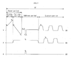
- FIG 3 is a detailed diagram illustrating a driving waveform supplied during a reset period, an address period, and a sustain period, as shown in Figure 2 .
- the PDP 106 displays a predetermined image by performing a reset period, an address period, and a sustain period, in order, generally during one sub-field (SF).
- SF sub-field
- a voltage of a Y electrode is gradually increased from a voltage Vs to a voltage Vset.
- An X electrode is maintained at a reference voltage 0V.
- a negative wall charge is formed in the Y electrode, and a positive wall charge is formed in the X and A electrodes.
- a voltage of the Y electrode is gradually decreased from the voltage Vs to a voltage Vnf.
- a voltage Ve is applied to the X electrode.
- a weak discharge occurs between the Y and X electrodes and between the Y and A electrodes, while the voltage of the Y electrode is decreased.
- a negative wall charge is maintained in the Y electrode, and the positive wall charges are erased from the X and A electrodes, so that discharge cells are initialized.
- is set to approximate a firing voltage between the Y and X electrodes.
- a wall voltage between the Y and X electrodes is nearly 0V, to prevent misfiring of the discharge cells, which have not been discharged during the address period, to allow such cells to be discharged during the sustain period.
- one or more discharge cells can be selected for subsequent emission, by applying various voltages thereto.
- the voltage Ve is applied to the X1 electrode
- a scan pulse with a voltage VscL is sequentially applied to the Y1 electrode.
- a Voltage Va is applied to the A1 electrode, passing through the selected discharge cell C.
- an address discharge occurs between the A1 electrode and the Y1 electrode and between the Y1 and the X electrode, so that a positive wall charge is formed in the Y1 electrode, and a negative wall charge is respectively formed in the A1 and X1 electrodes.
- the voltage VscL may be set as the same as or less than the voltage Vnf.
- the voltage VscH which is higher than the voltage VscL, is applied, and a reference voltage (0V in Figure 3 ) is applied to the A electrodes of unselected discharge cells.
- the scan driver 102 selects a Y electrode, to which a scan pulse with the voltage VscL will be applied, among the Y electrodes (Y1 to Yn). For example, in a case where a single cell is driven, a Y electrode may be selected in an order arranged in a vertical direction.
- the address driver 104 selects a discharge cell to be turned on, among discharge cells including the selected Y electrode. In other words, the address driver 104 selects a cell, to which an address pulse of a voltage Va will be applied, among the A electrodes (A1 to Am).
- a sustain pulse having a high voltage (the voltage Vs in Figure 3 ) and a low voltage (0V in Figure 3 ), is alternately applied to the Y and X electrodes, so that a sustain discharge occurs between the Y and X electrodes of the selected discharge cells.
- the number of the sustain pulses is selected according to the weight value of the respective sub-fields.
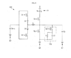
- FIG 4 is a circuit diagram illustrating a sustain pulse generating circuit 400, to generate a sustain pulse as shown in Figure 3 .
- a panel capacitor (Cp), in Figure 4 equivalently illustrates a capacitance component between X and Y electrodes.
- the X electrode of the panel capacitor (Cp) is indicated to be coupled to a ground terminal G1, but the X electrode is actually coupled to the sustain electrode driver 108.
- an element when it is described that an element is “coupled” to another element, the element may be “directly coupled” to the other element or “electrically coupled” to the other element through a third element.
- the element may be connected to the other element by a wire or other electrical connection.
- a first element when it is described that a first element is “coupled between” second and third elements, the first element may have a first contact, which is coupled to the second element, and the first element may have a second contact which is coupled to the third element.
- a first element "coupled between" second and third elements can refer to a series connection, with the first element being coupled in series between the second and third elements.
- a "contact”, as used herein, refers to an electrical connection or node.
- a transistor coupled to a contact which is coupled to an electrode and a capacitor, can refer to an connection between a wire connected to the transistor and a wire connected to the electrode and capacitor. Either wire can continue on and connect to other elements.
- the sustain pulse generating circuit 400 includes a recovery capacitor (Cerc), an inductor (L), transistors (Sr, Sf, Ss, and Sg), diodes (Dr and Df), and a discharge part 120.
- the transistor Ss is referred to as a first transistor
- the transistor Sg is referred to as a second transistor
- the transistor Sr is referred to as a third transistor
- the transistor Sf is referred to as a fourth transistor
- the diode Dr is referred to as a first diode
- the diode Df is referred to as a second diode.
- the recovery capacitor (Cerc) is coupled to the panel capacitor (Cp) and is to supply or recover predetermined charges.
- a cathode of the recovery capacitor (Cerc) is coupled to a ground terminal G3, and an anode of the recovery capacitor (Cerc) is coupled to a contact between the third and fourth transistors (Sr and Sf).
- the recovery capacitor (Cerc) can be referred to as a third power supply.
- One terminal of the inductor (L) is coupled to a contact between the first and second diodes (Dr and Df), and the other terminal is coupled to the panel capacitor (Cp).
- the inductor (L) and the panel capacitor (Cp) allow a resonance to be generated therebetween.
- the first transistor (Ss) includes: a drain coupled to a first power supply (P1) to supply a first voltage, i.e., a Vs voltage; a source coupled to the panel capacitor (Cp); and a gate coupled to a control signal terminal (not shown), to which a low or high level control signal is input.
- the second transistor (Sg) includes: a drain coupled to the panel capacitor (Cp); a source coupled to a second power supply, i.e., a ground terminal G2 to supply a second voltage, i.e., a ground voltage; and a gate coupled to a control signal terminal (not shown), to which a low or high level control signal is input.
- the third transistor (Sr) includes a drain coupled to the third power supply, i.e., the recovery capacitor (Cerc); a source coupled to the first diode (Dr); and a gate coupled to a control signal terminal (not shown), to which a low or high level control signal is input.
- the fourth transistor (Sf) includes: a drain coupled to the second diode (Df); a source coupled to the recovery capacitor (Cerc); and a gate coupled to a control signal terminal (not shown), to which a low or high level control signal is input.
- the first and second diodes (Dr and Df) are disposed to cut-off a current flow from a body diode (not shown), coupled to the third and fourth transistors (Sr and Sf).
- An anode of the first diode (Dr) is coupled to the third transistor (Sr), and a cathode of the first diode (Dr) is coupled to the inductor (L).
- An anode of the second diode (Df) is coupled to the inductor (L), and a cathode of the second diode (Df) is coupled to the fourth transistor (Sf).
- a diode (not shown) can be coupled between the first power supply P1, which is to supply the Vs voltage, and the inductor (L) to clamp a voltage of the other terminal of the inductor (L) to the Vs voltage.
- a diode (not shown) can be coupled between the ground terminal G2 and the inductor (L), to clamp a voltage of the other terminal of the inductor (L) to 0V.
- the discharge part 120 includes a transistor (Ssf), a bypass capacitor (Cf) and a discharge resistor (R).
- the transistor Ssf is referred to as a fifth transistor.
- the fifth transistor (Ssf) includes: a drain coupled to the panel capacitor (Cp); a source coupled to a contact of the discharge resistor (R) and to a capacitor, i.e., the bypass capacitor (Cf); and a gate coupled to a control signal terminal (not shown), from which a low or high level control signal is input.
- the fifth transistor (Ssf) is switched to supply a voltage stored in the inductor (L) to the bypass capacitor (Cf), before the second transistor (Sg), is turned on. Likewise, the voltage stored in the inductor (L), through the fifth transistor (Ssf), is minimized, so that the hard switching of the second transistor (Sg) may be minimized.
- the bypass capacitor (Cf) bypasses a high-frequency component of the voltage charge in the inductor (L) through the ground terminal G2, due to a decrease of impedance, if the high-frequency component is input through the fifth transistor (Ssf). Further, if a low-frequency component of the voltage stored in the inductor (L) is input through the fifth transistor (Ssf), the bypass capacitor (Cf) stores the low-frequency component, due to the increase of impedance.
- One terminal of the bypass capacitor (Cf) is coupled to the ground terminal G2, and the other is coupled to the fifth transistor (Ssf).
- the discharge resistor (R) consumes the voltage of the inductor (L), stored in the bypass capacitor (Cf), through the ground terminal G2, if the fifth transistor (Ssf) is turned off.
- the discharge resistor (R) is coupled in parallel with the bypass capacitor (Cf).
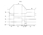
- Figure 5 is a diagram illustrating an operation timing for a sustain period, using the circuit as shown in Figure 4 .
- Figures 6A to 6E are diagrams illustrating current paths for respective periods, as shown in Figure 5 .
- the third transistor (Sr) is turned on when a high level control signal is applied to the third transistor (Sr). Then, referring to Figure 6A , a current path is formed from the recovery capacitor (Cerc), through the third transistor (Sr), the first diode (Dr), the inductor (L), and to the panel capacitor (Cp), so that a resonance occurs between the inductor (L) and the panel capacitor (Cp).
- the current stored in the recovery capacitor (Cerc) is moved to and is stored in the panel capacitor (Cp), by the above resonance.
- the voltage of a Y electrode of the panel capacitor (Cp) is gradually increased from 0V.
- a low level control signal is applied to the third transistor (Sr), and a high level control signal is applied to the first transistor (Ss), so that the first transistor (Ss) is turned on.
- a current path is formed from a Vs power supply, through the first transistor (Ss), and to the panel capacitor (Cp). Accordingly, the Vs voltage is applied to the Y electrode of the panel capacitor (Cp), through the first transistor (Ss).
- a low level control signal is applied to the first transistor (Ss), and a high level control signal is applied to the fourth transistor (Sf), so that the fourth transistor (Sf) is turned on.
- a current path is formed from the panel capacitor (Cp), through the inductor (L), the second diode (Df), the fourth transistor (Sf), and to the recovery capacitor (Cerc), so that a resonance occurs between the inductor (L) and the panel capacitor (Cp).
- the current stored in the panel capacitor (Cp) is moved to and is stored in the recovery capacitor (Cerc), by the above resonance, and the voltage of the Y electrode, of the panel capacitor (Cp), is gradually decreased from the Vs voltage.
- a low level control signal is applied to the fourth transistor (Sf), and a high level control signal is applied to the fifth transistor (Ssf), so that the fifth transistor (Ssf) is turned on.
- a turn-on period of the fifth transistor (Ssf) is shorter than that of the fourth transistor (Sf).
- a current path is formed from the inductor (L), through the fifth transistor (Ssf), and to the bypass capacitor (Cf). The voltage stored in the inductor (L) is applied to the bypass capacitor (Cf) through the fifth transistor (Ssf).
- a high-frequency component of about 30 to 100MHz, included in the voltage stored in the inductor (L), is applied to the bypass capacitor (Cf), the bypass capacitor (Cf) maintains in a short status, due to a decrease of impedance. Accordingly, the voltage stored in the inductor (L) is induced at the second voltage, i.e., a ground voltage, through the fifth transistor (Ssf) and the bypass capacitor (Cf). Further, a frequency component of less than 30MHz, included in the voltage stored in the inductor (L), is applied to the bypass capacitor (Cf), and the bypass capacitor (Cf) charges a voltage from the inductor (L), due to the increase of impedance.
- a low level control signal is applied to the fifth transistor (Ssf), and a high level control signal level is applied to the second transistor (Sg), so that the second transistor (Sg) is turned on.
- a current path is formed from the panel capacitor (Cp), through the second transistor (Sg) and to the ground terminal G3.
- a ground voltage is then applied to the Y electrode of the panel capacitor (Cp).
- the voltage stored in the bypass capacitor is induced at the ground voltage, through the discharge resistor (R).
- the plasma display device 100 allows the second transistor (Sg), which is coupled to a ground terminal G2, to be turned on after the voltage stored in the inductor (L) has been reduced through the discharge part 120, during the interval T3. Accordingly, the hard switching of the second transistor (Sg) is minimized, the associated EMI is reduced, and heat generated from the second transistor (Sg) is decreased about 5 to 10 degrees, in comparison with the related art. As described above, the plasma display device according to aspects of present invention minimizes the hard switching of a transistor coupled to a ground, thereby reducing the heat stress of the transistor and the electro magnetic interference (EMI) therefrom.
- EMI electro magnetic interference
Landscapes
- Engineering & Computer Science (AREA)
- Physics & Mathematics (AREA)
- Power Engineering (AREA)
- Plasma & Fusion (AREA)
- Computer Hardware Design (AREA)
- General Physics & Mathematics (AREA)
- Theoretical Computer Science (AREA)
- Control Of Indicators Other Than Cathode Ray Tubes (AREA)
- Control Of Gas Discharge Display Tubes (AREA)
Applications Claiming Priority (1)
| Application Number | Priority Date | Filing Date | Title |
|---|---|---|---|
| KR1020060117890A KR100824846B1 (ko) | 2006-11-27 | 2006-11-27 | 플라즈마 표시 장치 및 그 구동 방법 |
Publications (1)
| Publication Number | Publication Date |
|---|---|
| EP1930867A2 true EP1930867A2 (fr) | 2008-06-11 |
Family
ID=39281805
Family Applications (1)
| Application Number | Title | Priority Date | Filing Date |
|---|---|---|---|
| EP07121004A Withdrawn EP1930867A2 (fr) | 2006-11-27 | 2007-11-19 | Affichage à plasma et son procédé de commande |
Country Status (5)
| Country | Link |
|---|---|
| US (1) | US20080122374A1 (fr) |
| EP (1) | EP1930867A2 (fr) |
| JP (1) | JP2008134602A (fr) |
| KR (1) | KR100824846B1 (fr) |
| CN (1) | CN101192367A (fr) |
Family Cites Families (4)
| Publication number | Priority date | Publication date | Assignee | Title |
|---|---|---|---|---|
| JP3460496B2 (ja) | 1997-03-06 | 2003-10-27 | 三菱電機株式会社 | プラズマディスプレイの駆動装置 |
| JPH10268831A (ja) | 1997-03-27 | 1998-10-09 | Mitsubishi Electric Corp | プラズマディスプレイパネル用電力回収回路 |
| KR100670278B1 (ko) * | 2005-01-26 | 2007-01-16 | 삼성에스디아이 주식회사 | 디스플레이 패널의 구동장치 |
| KR20060090052A (ko) * | 2005-02-07 | 2006-08-10 | 엘지전자 주식회사 | 플라즈마 디스플레이 장치 및 플라즈마 디스플레이 패널의구동장치 |
-
2006
- 2006-11-27 KR KR1020060117890A patent/KR100824846B1/ko not_active Expired - Fee Related
-
2007
- 2007-08-23 JP JP2007217635A patent/JP2008134602A/ja not_active Withdrawn
- 2007-11-15 US US11/940,424 patent/US20080122374A1/en not_active Abandoned
- 2007-11-19 EP EP07121004A patent/EP1930867A2/fr not_active Withdrawn
- 2007-11-27 CN CNA2007101932766A patent/CN101192367A/zh active Pending
Also Published As
| Publication number | Publication date |
|---|---|
| JP2008134602A (ja) | 2008-06-12 |
| US20080122374A1 (en) | 2008-05-29 |
| KR100824846B1 (ko) | 2008-04-23 |
| CN101192367A (zh) | 2008-06-04 |
Similar Documents
| Publication | Publication Date | Title |
|---|---|---|
| US6304038B1 (en) | Apparatus for driving a display panel | |
| US8111211B2 (en) | Plasma display comprising at least first and second groups of electrodes and driving method thereof | |
| US7642994B2 (en) | Plasma display | |
| EP1755101A2 (fr) | Appareil d'affichage à plasma | |
| EP1930867A2 (fr) | Affichage à plasma et son procédé de commande | |
| US8125413B2 (en) | Plasma display device and driving method thereof | |
| JP4473518B2 (ja) | プラズマディスプレイパネル駆動装置 | |
| KR100824861B1 (ko) | 플라즈마 디스플레이 장치 및 구동 방법 | |
| KR20090050690A (ko) | 플라즈마 표시 장치 및 그 구동 장치 | |
| EP1939845A2 (fr) | Dispositif à écran plasma et procédé de commande associé | |
| US20080170001A1 (en) | Plasma display and associated driver | |
| KR100759463B1 (ko) | 플라즈마 표시 장치 및 그 구동 방법 | |
| US20080143642A1 (en) | Plasma display device and driving apparatus thereof | |
| EP1901266A2 (fr) | Dispositif d'affichage à plasma et procédé de commande | |
| KR100740095B1 (ko) | 플라즈마 표시 장치 및 그 구동 방법 | |
| KR100943956B1 (ko) | 플라즈마 표시 장치 및 그 구동 장치 | |
| CN101609640A (zh) | 等离子体显示器及其驱动方法 | |
| KR100627410B1 (ko) | 플라즈마 표시 장치 및 그 구동 방법 | |
| US20080158104A1 (en) | Plasma display device | |
| KR100859698B1 (ko) | 플라즈마 표시 장치 및 그 구동 방법 | |
| JP4416418B2 (ja) | プラズマディスプレイパネル駆動装置 | |
| KR100998090B1 (ko) | 플라즈마 표시 장치 | |
| US20080165175A1 (en) | Plasma display and driving method thereof | |
| KR20090119199A (ko) | 플라즈마 표시 장치 및 그 구동 방법 | |
| JP2004309616A (ja) | 表示パネル駆動装置 |
Legal Events
| Date | Code | Title | Description |
|---|---|---|---|
| PUAI | Public reference made under article 153(3) epc to a published international application that has entered the european phase |
Free format text: ORIGINAL CODE: 0009012 |
|
| 17P | Request for examination filed |
Effective date: 20071119 |
|
| AK | Designated contracting states |
Kind code of ref document: A2 Designated state(s): AT BE BG CH CY CZ DE DK EE ES FI FR GB GR HU IE IS IT LI LT LU LV MC MT NL PL PT RO SE SI SK TR |
|
| AX | Request for extension of the european patent |
Extension state: AL BA HR MK RS |
|
| RAP1 | Party data changed (applicant data changed or rights of an application transferred) |
Owner name: SAMSUNG SDI CO., LTD. |
|
| STAA | Information on the status of an ep patent application or granted ep patent |
Free format text: STATUS: THE APPLICATION HAS BEEN WITHDRAWN |
|
| 18W | Application withdrawn |
Effective date: 20091106 |