EP1930965A1 - Elektrolumineszenzvorrichtung und Elektrolumineszenztafel - Google Patents
Elektrolumineszenzvorrichtung und Elektrolumineszenztafel Download PDFInfo
- Publication number
- EP1930965A1 EP1930965A1 EP07075918A EP07075918A EP1930965A1 EP 1930965 A1 EP1930965 A1 EP 1930965A1 EP 07075918 A EP07075918 A EP 07075918A EP 07075918 A EP07075918 A EP 07075918A EP 1930965 A1 EP1930965 A1 EP 1930965A1
- Authority
- EP
- European Patent Office
- Prior art keywords
- light
- light scattering
- light emitting
- electrode
- scattering portion
- Prior art date
- Legal status (The legal status is an assumption and is not a legal conclusion. Google has not performed a legal analysis and makes no representation as to the accuracy of the status listed.)
- Withdrawn
Links
Images




Classifications
-
- H—ELECTRICITY
- H10—SEMICONDUCTOR DEVICES; ELECTRIC SOLID-STATE DEVICES NOT OTHERWISE PROVIDED FOR
- H10K—ORGANIC ELECTRIC SOLID-STATE DEVICES
- H10K50/00—Organic light-emitting devices
- H10K50/10—OLEDs or polymer light-emitting diodes [PLED]
- H10K50/11—OLEDs or polymer light-emitting diodes [PLED] characterised by the electroluminescent [EL] layers
- H10K50/125—OLEDs or polymer light-emitting diodes [PLED] characterised by the electroluminescent [EL] layers specially adapted for multicolour light emission, e.g. for emitting white light
-
- H—ELECTRICITY
- H05—ELECTRIC TECHNIQUES NOT OTHERWISE PROVIDED FOR
- H05B—ELECTRIC HEATING; ELECTRIC LIGHT SOURCES NOT OTHERWISE PROVIDED FOR; CIRCUIT ARRANGEMENTS FOR ELECTRIC LIGHT SOURCES, IN GENERAL
- H05B33/00—Electroluminescent light sources
- H05B33/12—Light sources with substantially two-dimensional [2D] radiating surfaces
- H05B33/22—Light sources with substantially two-dimensional [2D] radiating surfaces characterised by the chemical or physical composition or the arrangement of auxiliary dielectric or reflective layers
-
- B—PERFORMING OPERATIONS; TRANSPORTING
- B82—NANOTECHNOLOGY
- B82Y—SPECIFIC USES OR APPLICATIONS OF NANOSTRUCTURES; MEASUREMENT OR ANALYSIS OF NANOSTRUCTURES; MANUFACTURE OR TREATMENT OF NANOSTRUCTURES
- B82Y20/00—Nanooptics, e.g. quantum optics or photonic crystals
-
- B—PERFORMING OPERATIONS; TRANSPORTING
- B82—NANOTECHNOLOGY
- B82Y—SPECIFIC USES OR APPLICATIONS OF NANOSTRUCTURES; MEASUREMENT OR ANALYSIS OF NANOSTRUCTURES; MANUFACTURE OR TREATMENT OF NANOSTRUCTURES
- B82Y30/00—Nanotechnology for materials or surface science, e.g. nanocomposites
-
- H—ELECTRICITY
- H10—SEMICONDUCTOR DEVICES; ELECTRIC SOLID-STATE DEVICES NOT OTHERWISE PROVIDED FOR
- H10K—ORGANIC ELECTRIC SOLID-STATE DEVICES
- H10K59/00—Integrated devices, or assemblies of multiple devices, comprising at least one organic light-emitting element covered by group H10K50/00
- H10K59/10—OLED displays
- H10K59/17—Passive-matrix OLED displays
- H10K59/173—Passive-matrix OLED displays comprising banks or shadow masks
-
- H—ELECTRICITY
- H10—SEMICONDUCTOR DEVICES; ELECTRIC SOLID-STATE DEVICES NOT OTHERWISE PROVIDED FOR
- H10K—ORGANIC ELECTRIC SOLID-STATE DEVICES
- H10K59/00—Integrated devices, or assemblies of multiple devices, comprising at least one organic light-emitting element covered by group H10K50/00
- H10K59/80—Constructional details
- H10K59/875—Arrangements for extracting light from the devices
- H10K59/877—Arrangements for extracting light from the devices comprising scattering means
-
- H—ELECTRICITY
- H10—SEMICONDUCTOR DEVICES; ELECTRIC SOLID-STATE DEVICES NOT OTHERWISE PROVIDED FOR
- H10K—ORGANIC ELECTRIC SOLID-STATE DEVICES
- H10K2102/00—Constructional details relating to the organic devices covered by this subclass
- H10K2102/301—Details of OLEDs
- H10K2102/331—Nanoparticles used in non-emissive layers, e.g. in packaging layer
Definitions
- the present invention relates to an electroluminescent (EL) device improved in luminous efficiency (efficiency of extracting light), such as an organic EL device and an inorganic EL device, and to an electroluminescent panel using the same.
- EL electroluminescent
- An EL display unit particularly an organic EL display unit, has advantages of wide viewing angle and high speed of response because of a self-luminous device. Also, a backlight unit is unnecessary, allowing for a thinner and lighter-weight display unit. In view of these points, recently, an organic EL display unit attracts attention as an alternative to a liquid crystal display unit, and further for illumination.
- An organic EL device which is a main part of an organic EL display unit, includes an optically transparent front electrode, a back electrode that is opposed to the front electrode, and light reflective or optically transparent, and an organic substance layer including a light emitting layer intervening in them.
- the organic EL device is a self-luminous device of charge injection type that produces luminescence due to electric current flowing in the organic substance layer.
- To display on the organic EL display unit it is necessary to cause light emitted from a light emitting medium to exit from the front electrode.
- a component of the light from the light emitting medium propagating in the direction parallel to the two electrodes and a component totally reflected by an interface between a transparent substrate on the side of extracting light and the atmosphere have a large light intensity. Therefore light exiting from the front face of the device loses light intensity, and the quantity of lost light reaches 70 to 80% of the total quantity of light, from the measurement results.
- a quantity of light in thin film propagation is 50% of the total quantity of emitted light
- a quantity of light in substrate propagation is 30%
- a quantity of light extracted externally is small to the degree of about 20% (see G. Gu, S. R. Forrest, Optics Lett., 22 (1997) 396 ).
- much of light emitted from an emitting layer cannot be extracted externally from the organic EL device, presenting a problem of low efficiency of extracting light.
- JP-A-11-283751 describes that, in light traveling to a front face in a device, light traveling to a region having a wide angle is refracted by using a diffraction device or a zone plate to pass through an interface of a front electrode.
- This technique can enhance the efficiency of extracting light of an organic EL device.
- images may be improperly displayed as an organic EL display unit, because a pattern constituting the diffraction device or the zone plate has directional characteristics, so that directivity of extracted light changes dependent on the direction.
- fine features of the diffraction device or the zone plate have to be formed by lithography etc., also causing a problem of an increased cost.
- Another approach to enhancing the efficiency of extracting light includes, for example, a proposed method using a fine particle dispersion layer ( JP-A-2006-107744 ).
- the fine particle dispersion layer is provided between a transparent substrate and a front electrode, light emitted in a light emitting layer is reflected by both electrodes to propagate in the lateral direction.
- the fine particle dispersion layer is situated in the direction of extracting light, light exiting in the front direction is scattered to generate a component of light having an angle of not smaller than a critical angle, presenting a problem in terms of a decreased light emitting rate. Therefore, the efficiency of extracting light of a device including the conventional fine particle dispersion layer is not sufficiently enhanced.
- JP-A-06-151061 discloses an EL device made of substantially the same material as a light emitting layer of an inorganic EL device, formed continuously with the light emitting layer, and including a light propagating layer having light scattering means for scattering light propagating from the light emitting layer outside of the device. Concerning the light scattering means, it is described that a scattering particle is dispersed in the light propagating layer, but it is not disclosed how the scattering particle is dispersed in the light propagating layer.
- Another related art includes an art disclosed in JP-A-2003-303677 .
- the present invention has been made in view of the circumstances described above, and an object thereof is to provide an EL device (organic EL device) having luminous efficiency (efficiency of extracting light) enhanced.
- the present invention to solve the problems described above provides an electroluminescent device and an electroluminescent panel including:
- a light scattering medium is not provided in the direction of a film thickness (longitudinal direction) of the light emitting medium, but provided in the lateral direction of the light emitting medium.
- the EL device of the present invention because a component of emitted light having a large exit angle can be effectively extracted externally, an EL device and an EL panel improved in efficiency of extracting light can be provided.
- FIG. 1 is a conceptual diagram for describing a configuration of an EL device of a first exemplary embodiment according to the present invention.
- a first electrode 2 is formed in stripe geometry, and a light emitting medium 3 is sandwiched between the first electrode 2 and a second electrode 4 opposite to it.
- electron holes and electrons are recombined in the light emitting medium 3 to emit light.
- the emitted light is extracted externally in a direction A through the optically transparent first electrode 2 and support substrate 1.
- a part of the emitted light in the light emitting medium 3 exits in direction B, and further, is reflected by an interface of the support substrate 1 and the atmosphere, also reflected by an interface of the support substrate 1 and the first electrode 2, and further incident on a light scattering portion 5 containing a light scattering fine particle 5a on the side of the light emitting medium 3.
- the light scattering portion 5 contains at least the light scattering fine particle 5a and is formed in a tapered shape (trapezoidal). At this time, because the light scattering fine particle 5a is contained in the light scattering portion 5, the incoming light from the direction B is scattered, and thereby, also from the light scattering portion 5, the light can be extracted in the direction A of extracting light.
- the shape of the light scattering portion 5 is tapered, there is not an air gap between the light scattering portion 5 and the light emitting medium 3 formed after forming the light scattering portion 5, providing an advantage of excellently guiding a wave to the light scattering portion 5.
- the second electrode formed to bridge across each pixel in the direction perpendicular to the first electrode there is also brought out an advantage that the second electrode can be formed without breaking of wire, because the light scattering portion 5 is formed in the tapered shape.
- the light scattering portion 5 contains only the light scattering fine particle 5a, an emission wavelength in the light emitting medium 3 can be directly extracted from the light scattering portion 5 in the direction A of extracting light.
- fluorescent substance (5b) may also be added to the light scattering portion 5, in addition to the light scattering fine particle 5a, and in this case, light incident on the light scattering portion 5 is scattered by the light scattering fine particle and excites the fluorescent substance to produce fluorescence, and then the light can be extracted in the direction A of extracting light, as light having a different wavelength from the emission wavelength in the light emitting medium 3.
- FIG. 2 is a conceptual diagram for describing a configuration of an EL device of a second exemplary embodiment of the present invention.
- Points different from the first exemplary embodiment shown in FIG. 1 reside in that a light emitting portion contains a light emitting medium 3 for emitting blue light, and includes a first light scattering portion 5-1 in a direction B toward the light emitting medium 3, and a second light scattering portion 5-2 using fluorescent substance different from fluorescent substance of the first light scattering portion in a direction C opposite to the direction B, in which the first light scattering portion 5-1 and the second light scattering portion 5-2 have a luminescent color different from each other, and three kinds of pixel are used, that is, a blue (B) pixel contained in the light emitting portion, a green (G) pixel in the first light scattering portion 5-1 and a red (R) pixel in the second light scattering portion 5-2.
- blended light which is emitted by using a configuration including the three kinds of pixel (three primary colors) of the light emitting
- the first and second exemplary embodiments have been described referring to the case where the direction A of extracting light is set to the direction from the side of the support substrate 1 as an example, but not limited to this, the light may be extracted in the direction opposite to the direction toward the support substrate 1, or also in both directions.
- material provided on the side of extracting light is transparent material, and a light reflecting layer is provided on the opposite side.
- the light reflecting layer is preferably a reflecting electrode formed of an electrode on the side different from the side of extracting light, more preferably a reflecting electrode extending also on the side of the light scattering portion.
- a reflecting electrode is desirably formed to surround an upper end portion of the trapezoidal, light scattering portion, enhancing a photon confinement effect.
- the description described above has shown an example that, in a gap in the first electrode formed in the stripe geometry, the light scattering portion is formed similarly in the stripe geometry, but the light scattering portion, similarly to a fluorescent film disclosed in JP-A-2005-71920 described above, may be formed to surround the light emitting portion.
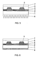
- the light scattering portion 5 is formed to surround the light emitting portion (light emitting medium 3).
- a tapered plane 5' is formed on the inside in contact with the light emitting medium 3. Further, in FIG.
- the first light scattering portion 5-1 and the second light scattering portion 5-2 are formed to surround the light emitting portion (light emitting medium 3), and a tapered plane 5-1' and a tapered plane 5-2' are formed on the inside of each of them.
- a tapered plane 5-1' and a tapered plane 5-2' are formed on the inside of each of them.
- FIGS. 5, 6 show also an example that, on the second electrode 4, sealing material 6 using material such as ultraviolet curing resin and a protective substrate 7 such as a glass substrate are formed. Also, in these examples, on the side of the support substrate 1, the microfabricated resin medium 8 or the light scattering medium 9 are provided, but they may be provided on the side of the protective substrate 7, when the direction of extracting light is the direction opposite to the direction toward the support substrate.
- a system for driving each pixel includes a conventionally known system such as a simple matrix system or an active matrix system having an active device such as a thin-film transistor (TFT) for switching each pixel.
- TFT thin-film transistor
- any of the first electrode and the second electrode may also be formed entirely as a common electrode.
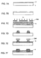
- transparent, electrically conductive material such as indium tin oxide (ITO) is deposited on a transparent substrate 1 to form a film (process (A)), and the film is pattered in stripe geometry to form the first electrode 2 (process (B)).
- binder material containing the light scattering fine particle 5a, or the light scattering fine particle 5a and fluorescent substance 5b is entirely applied (process (C)), and the binder material is pattered by photolithography technique to open a portion above the first electrode 2 formed in the stripe geometry.
- the binder material contains the light scattering fine particle 5a
- a resultant shape of the pattern is likely to be different from a rectangular pattern usually created by photolithography technique.
- a negative photosensitive resin is used as the binder material and a photomask PM is used to expose, and subsequently, an aromatic organic solvent is used to develop.
- the tapered shape can be controlled. That is, in the upper portion, a width thereof will be formed as specified by the mask PM, but as approaching the lower portion, light is more scattered, so-called a skirt shape is provided.
- a density of cross-linkage becomes lower, as approaching the lower portion, when the developing time is shortened, a forward tapered shape (trapezoidal shape) expanding downward (toward the first electrode) from an exposed surface is formed, and as the developing time is longer, the lower portion having a lower density of cross-linkage is more easily removed.
- the light scattering portion 5 in the forward tapered shape can be provided (process (D)).
- the photosensitive resin used for the binder material it is preferably processed by heat.
- a deposition mask DM is placed over the light scattering portion 5 to shield and the light emitting medium 3 is formed on the first electrode 2 by means of vacuum deposition etc. (process (E)). Then, metal for the second electrode is formed in a shape of the second electrode by means of deposition etc. through a mask for the second electrode (not shown) (process (F)). Subsequently, a layer of sealing material (not shown) and a substrate etc. are laminated to form an EL device. Further, by providing electrical connection to each electrode, a control circuit and a power supply etc., an EL panel is finished.
- the first electrode 2 was formed on the support substrate 1, but on the contrary, the second electrode 4 may be formed on the support substrate 1, and the light emitting medium 3 and the first electrode 2 may be formed.
- a specific configuration includes configurations shown in FIGS. 8 to 10 .
- the configuration made by using the method shown in FIG. 7 and the first electrode 2 is a transparent electrode, the second electrode 4 is formed as a reflecting electrode, and the direction A of extracting light is the direction toward the support substrate 1.
- a region where the light emitting medium 3 is formed is a light emitting portion.
- Light emitted by the light emitting portion is divided into light mainly extracted directly in the direction A of extracting light and light traveling in the lateral direction B, and the light in the direction B can be incident on the light scattering portion 5 and scattered by the light scattering fine particle 5a, or absorbed by the fluorescent substance 5b and extracted in the direction A as light having another wavelength.
- light reflected by an interface between the first electrode 2 and the support substrate 1, an interface between the support substrate 1 and the atmosphere, and a surface of the second electrode 4 can be also incident on the light scattering portion 5 and extracted in the direction A of extracting light.
- FIG. 9 shows an exemplary embodiment that light is extracted in the direction opposite to the direction toward the support substrate 1, and also an exemplary embodiment that the second electrode 4 is formed on the support substrate and the first electrode 2 is formed on the light emitting medium 3. Also in this case, light coming from the light emitting portion in the direction B is scattered or converted into light having another wavelength in the light scattering portion 5, and extracted in the direction A of extracting light.
- FIG. 10 shows an exemplary embodiment that the second electrode 4, which is formed to cover the light scattering portion 5 in the exemplary embodiment shown in FIG. 8 , does not have its electrode formed on the light scattering portion 5.
- the direction in which light can be extracted includes both the direction A 1 from the side of the support substrate 1 and the direction A 2 opposite to the support substrate 1.
- the reflective electrode is preferably formed to overlap with the light scattering portion 5, and especially, as shown in FIG. 8 , the reflective electrode is preferably formed to cover the upper end portion of the trapezoidal, light scattering portion, because the photon confinement effect becomes high and the efficiency of extracting light in the light scattering portion 5 is enhanced.
- the support substrate is a member for supporting the light emitting portion and the light scattering portion, and for that purpose, is preferably a member having superior mechanical strength and dimensional stability.
- Material for the support substrate is selected from inorganic material and organic material.
- Inorganic material includes, for example, a glass plate, a metal plate and a ceramic plate.
- Organic material includes various resin plates. Transparent material is used when light is extracted from the side of the support substrate.
- the first electrode plays a role as a positive electrode in mainly injecting electron holes into the light emitting medium, and in the organic EL device, material having a work function having not smaller than 4.5 eV is effective.
- material having a work function having not smaller than 4.5 eV is effective.
- metals and oxides thereof such as indium tin oxide (ITO) alloy, tin oxide (NESA), gold, silver, platinum and copper, and mixture thereof are usable.
- Optically transparent material such as ITO is used when light is extracted from the side of the support substrate.
- the second electrode plays a role as a negative electrode in mainly injecting electrons into the light emitting medium, and in the organic EL device, material having a work function having a small value is effective.
- material having a work function having a small value is effective.
- indium, aluminum, magnesium, magnesium-indium alloy, magnesium-aluminum alloy, aluminum-lithium alloy, aluminum-scandium-lithium alloy, magnesium-silver alloy and mixture thereof are usable.
- the light emitting medium is a medium containing a light emitting layer where electrons and electron holes can be recombined to produce EL, and is divided into an organic system and an inorganic system dependent on material used.
- the EL device includes, for example, the following layer configurations.
- the light emitting layer may be formed of a plurality of layers that emit different colors from each other, respectively.
- Luminescent material used for the organic EL device especially has no limitation, and any of chemical compounds usually used for luminescent material is usable.
- any of chemical compounds usually used for luminescent material is usable.
- Electron hole transporting material used for the present invention especially has no limitation, and any of chemical compounds usually used for electron hole transporting material may be used.
- triphenyl diamines such as bis(di(p-tolyl)aminophenyl)-1,1-cyclohexane, 4,4'-bis(m-tolylphenylamino)biphenyl (TPD), N,N'-diphenyl-N,N'-bis(1-naphthyl)-1,1'-biphenyl)-4,4'-diamine ( ⁇ -NPD), and molecules of star-burst type are included.
- triphenyl diamines such as bis(di(p-tolyl)aminophenyl)-1,1-cyclohexane, 4,4'-bis(m-tolylphenylamino)biphenyl (TPD), N,N'-diphenyl-N,N'-bis(1-naphthy
- Electron transporting material used for the present invention especially has no limitation, and any of chemical compounds usually used for electron transporting material may be used.
- oxadiazole derivatives such as 2-(4-biphenylyl)-5-(4-t-butylphenyl)-1,3,4-oxadiazole (Bu-PBD) and OXD-7, triazole derivatives, and metal complexes of quinolinol system are included.
- luminescent material used for the inorganic EL device especially has no limitation, and conventionally known material is usable.
- conventionally known material is usable.
- calcium thiogallate to which cerium (Ce) is added CaGa 2 S 4 : Cs
- strontium sulfide to which copper (Cu) is added SrS: Cu
- the light scattering portion includes at least one kind of fine particle and at least one kind of binder material.
- the fine particle has fine particles (light scattering fine particles) having a light scattering function in the visible region dispersed therein.
- Fluorescent substance may be dispersed or dissolved in the binder material.
- the refractive index of the light scattering portion is preferably higher than at least any one of those of the light emitting medium, the first electrode and the second electrode.
- a film thickness of the light scattering portion especially has no limitation, and the film thickness may be formed thick sufficiently at least to form the light emitting portion using means such as deposition. Typically, the film thickness is formed to be 0.1 ⁇ m to 50 ⁇ m. An amount of the at least one kind of fine particle contained in the light scattering portion is preferably 0.1% to 80% by volume.
- a higher refractive index of the fine particle than that of the binder material can control the refractive index of the light scattering portion at concentration of contained fine particle.
- the light scattering fine particle has especially no limitation in relation to material as long as a wavelength in the visible region is scattered, and the material thereof preferably includes inorganic oxide such as TiO 2 , ZrO 2 and ZnO, inorganic nitride, inorganic oxynitride, and metal fine particles of Au, Pt and Ag, and the average grain size is preferably 100 to 400 nm.
- any substance that can absorb emitted light in the light emitting portion to produce fluorescence is usable.
- the fluorescent substance may be divided into organic fluorescent substance and inorganic fluorescent substance.
- the organic fluorescent substance as a general rule, has a high fluorescence yield, and on the one side, the inorganic fluorescent substance is superior in durability.
- a fluorescent wavelength of the fluorescent substance generally appears on the side of a long wave of an absorption wavelength (incident light). Accordingly, fluorescent substance that can absorb emitted light in the light emitting medium (light in the ultraviolet region may be included, in addition to light in the visible region) to produce fluorescence having a desired wavelength is suitably selected.
- white luminescence can be produced by using fluorescent substance that produces fluorescence having a complementary color to the emitted light in the light emitting medium in combination with the light emitting medium, and luminescence of various colors including white light can be produced by adjusting an additive amount of fluorescent substance, where the emitted light in the light emitting medium is blue light, and two different, fluorescent colors in the light scattering portion are red and green, as shown in FIG. 2 .
- the organic and inorganic fluorescent substance may include ones described in JP-A-2005-71920 described above. Further, for the inorganic fluorescent substance, fine particle-like substance may be preferably used, and in this case, the average grain size is preferably 50 nm to 10 ⁇ m.
- the binder described above may be selected from inorganic compounds and organic compounds having light transparency.
- the inorganic compounds may include inorganic oxide, inorganic nitride and inorganic oxynitride.
- the organic compounds may include various resin material, and are preferably resin material having photosensitivity because of easy processing. For the resin material having photosensitivity, various, light transparent resist material may be used. Also, the binder material itself may have luminescence. Such binder material may include resin material in which a luminescent compound residue is introduced into side chains of high polymer.
- external quantum efficiency may be obtained from the following expression, based on a ratio of the number of photons (Np) radiated externally from the EL device per unit time to the number of electrons (Ne) injected into the EL device per unit time.
- External quantum efficiency Np / Ne
- Np may be obtained from measurement of optical spectrum, and in the present invention, the measurement was conducted in an integrated sphere.
- the EL device was manufactured according to the processes shown in FIG. 7 .
- a transparent glass substrate (non-alkali glass NA35 from NH TECHNO GLASS CORPORATION) having a length of 50 mm x a width 50 mm and a thickness of 0.7 mm was prepared. After this transparent glass substrate was ultrasonically cleaned using acetone and pure water, and dried, a transparent electrode having a thickness of 130 nm was formed by spattering indium tin oxide (ITO) entirely thereon (process (A)).
- ITO indium tin oxide
- photosensitive resist OFPR-800 from TOKYO OHKA KOGYO CO., LTD.
- photosensitive resist OFPR-800 from TOKYO OHKA KOGYO CO., LTD.
- processes of mask exposing, developing (using NMD3 (developer) from TOKYO OHKA KOGYO CO., LTD.) and etching were carried out, forming the first electrode having a width of 70 ⁇ m and a pitch of 100 ⁇ m in a stripe pattern (process (B)).
- the refractive index of the support substrate was 1.5 and the refractive index of the first electrode was 1.8.
- photosensitive negative photoresist resist of isopropylene rubber base; name of article "OMR”
- OMR optical magnetic resonance
- the photoresist was heated by an oven to remove solvent therefrom, and exposed using a photomask having a width of 15 ⁇ m and a pitch of 100 ⁇ m, then developed for five minutes, making a forward tapered structure.
- xylene was used for developing.
- SEM scanning electron microscope
- it was cleaned using butyl acetate.
- heat treatment was performed at 150°C for 30 minutes. This light scattering portion had a height of 8 ⁇ m and the refractive index of the light scattering portion was 1.9.
- the light scattering portion was covered with a mask, and the light emitting medium including an electron hole transporting layer, an yellow light emitting layer, a blue light emitting layer and an electron transporting layer was formed on the first electrode (process (F)).
- electron hole transporting material ⁇ -NPD (from CHEMIPRO KASEI KAISHA, LTD.)
- ⁇ -NPD and rubrene were deposited by means of double evaporation by a thickness of 20 nm with a film thickness ratio of rubrene being 5%.
- Ag Ag was deposited by a thickness of 100 nm, forming the second electrode.
- it was sealed with a glass substrate and UV curing resin separately prepared, manufacturing the EL device (process (G)).
- the EL panel produced white light, and at this time, the external quantum efficiency was about 2.2%.
- An EL device was manufactured similarly to Example 1, but the fine particles TiO 2 were not contained in the light scattering portion, and also a mask having a width of 30 ⁇ m and a pitch of 100 ⁇ m was used as the photomask.
- the light scattering portion was formed to be a rectangular shape having a width of 30 ⁇ m.
- the EL panel produced white light, and at this time, the external quantum efficiency was about 1.6%. Comparing to the results of Example 1, it was found that providing the light scattering portion in which the fine particles having a light scattering function were dispersed improved the efficiency of extracting light.
- a light scattering portion was formed according to the processes similar to Example 1, but red fluorescent pigments (rhodamine 6G from Sigma-Aldrich Co.) were added to the binder material containing the fine particles TiO 2 of Example 1. Subsequently, an EL device having the light emitting portion including the electron hole transporting layer, the blue light emitting layer and the electron transporting layer, but not the yellow light emitting layer was made according to the processes similar to Example 1. A thickness of the blue light emitting layer was set to 50 nm. When a voltage of 8 V was applied to this EL device, the EL panel produced white light, and at this time, the external quantum efficiency was about 2.5%.
- An EL device was manufactured similarly to Example 2, but the fine particle TiO 2 was not contained in the light scattering portion and a mask having a width of 30 ⁇ m and a pitch of 100 ⁇ m was used as the photomask.
- the light scattering portion was formed to be a rectangular shape having a width of 30 ⁇ m.
- the EL panel produced white light, and at this time, the external quantum efficiency was about 2.3%. Comparing to the results of Example 2, it was found that, by dispersing the fine particles having a light scattering function, in addition to the fluorescent substance, the efficiency of extracting light was improved.
- An EL device was manufactured similarly to Example 2, except that a mask having a width of 30 ⁇ m and a pitch of 100 ⁇ m was used as the photomask, and a shape of the light scattering portion of Example 2 was formed by adjusting the developing time to have a height of 8 ⁇ m, a width of the lower portion (on the side of the support substrate) of 30 ⁇ m and a width of the upper portion of 30 ⁇ m.
- a voltage of 8 V was applied to this EL device, the EL panel produced white light, and at this time, the external quantum efficiency was about 2.4%. Comparing to Example 2, it was found that a trapezoidal shape of the light scattering portion brought out a higher efficiency of extracting light.
- An EL device was manufactured similarly to Example 2, except that a mask having a width of 30 ⁇ m and a pitch of 100 ⁇ m was used as the photomask, and a shape of the light scattering portion of Example 2 was formed by adjusting the developing time to have a height of 8 ⁇ m, a width of the lower portion (on the side of the support substrate) of 15 ⁇ m, and a width of the upper portion of 30 ⁇ m.
- a voltage of 8 V was applied to this EL device, the EL panel produced white light, and at this time, the external quantum efficiency was about 2.4%.
- a first light scattering portion and a second light scattering portion were formed according to the processes of the photolithography process similar to Example 1 by adding red, fluorescent pigments (rhodamine 6G from Sigma-Aldrich Co.) to the binder material containing the fine particles TiO 2 of Example 1 and separately using a solvent in which green, fluorescent pigments (coumarin 6 from Sigma-Aldrich Co.) was added to the binder material containing the fine particles TiO 2 so that the first light scattering portion containing rhodamine 6G and the second light scattering portion containing coumarin 6 were formed alternately to the first electrode ( FIG. 2 ).
- an EL device emitting blue light was made according to the processes similar to Example 2. When a voltage of 8 V was applied to this EL device, the EL panel produced white light, and at this time, the external quantum efficiency was about 2.6%. From the results, it was found that emitting the three primary colors more improved the efficiency of extracting light.
- a light scattering portion was formed according to the processes similar to Example 1 by dispersing inorganic, fluorescent substance fine particles (YAG) in the binder material containing the fine particles TiO 2 of Example 1. Subsequently, an EL device emitting blue light was made according to the processes similar to Example 2. When a voltage of 8 V was applied to this EL device, the EL panel produced white light, and at this time, the external quantum efficiency was about 2.4%. As the results, even if inorganic, fluorescent substance having a lower fluorescence yield than that of organic, fluorescent substance was used, by dispersing the fine particles having a light scattering function in the light scattering portion, the efficiency of extracting light was accomplished to a comparative level as the case where only the organic, fluorescent substance was used (second comparative example).
- a microfabricated film (quadrangular pyramid having a vertex angle of 90° and a pitch of 20 ⁇ m) was attached to the support substrate of the EL device manufactured similarly to Example 2 ( FIG. 5 ).
- the EL panel produced white light, and at this time, the external quantum efficiency was about 2.8%. From the results, it was found that further attaching the microfabricated film to the support substrate improved the efficiency of extracting a component of light that propagated in the substrate.
- a light scattering portion was formed by adding red, fluorescent pigments (rhodamine 6G from Sigma-Aldrich Co.) to the binder material containing the fine particles TiO 2 of Example 1 so that a square opening of 70 ⁇ m x 70 ⁇ m was formed with a frame having a width of 15 ⁇ m being left in the outer circumference, in a square of 100 ⁇ m ⁇ 100 ⁇ m at a pitch of 100 ⁇ m ( FIG. 3 ).
- an EL device emitting blue light was made according to the processes similar to Example 2. When a voltage of 8 V was applied to this EL device, the EL panel produced white light, and at this time, the external quantum efficiency was about 2.6%.
- a light scattering portion was formed according to the processes similar to Example 1, by adding red, fluorescent pigments (rhodamine 6G from Sigma-Aldrich Co.) to the binder material containing the fine particles TiO 2 of Example 1. Subsequently, an EL device emitting blue light was manufactured according to the processes similar to Example 2, but the second negative electrode was not formed on the light scattering portion. When a voltage of 8 V was applied to this EL device, the EL panel produced white light, and at this time, the external quantum efficiency was about 2.3%. From the results, it was found that the case of providing the second electrode for forming a reflecting electrode on the light scattering portion (Example 2) brought out a better effect of extracting light due to the photon confinement effect.
- red, fluorescent pigments rhodamine 6G from Sigma-Aldrich Co.
- Example 2 An inorganic EL device having a similar light scattering portion to that of Example 1 was manufactured, except that fluorescent substance in a luminescence center as a light emitting medium was CaGa 2 S 4 : Ce. When this EL device was operated at 8 V and 60 Hz, the external quantum efficiency was about 0.8%.
- Example 8 From the results of Example 8 and Comparative Example 5, it was found that, even in the inorganic EL device, dispersing the fine particles having a light scattering function in the light scattering portion improved the efficiency of extracting light.
- An EL device was formed according to the processes similar to Example 2, except that the first electrode was a reflecting electrode having Cr deposited entirely on the support substrate and the second electrode was a transparent electrode made of ITO. When a voltage of 8 V was applied to this EL device, the EL panel produced white light, and at this time, the external quantum efficiency was about 2.3%. Comparing to Example 2, it was found that providing the reflective electrode to surround the trapezoidal, upper portion of the light scattering portion more improved the efficiency of extracting light.
- Such organic EL apparatus can realize, for example, various electronics such as an illumination light source and a backlight unit having low power consumption and high brightness, a TV that can display high-quality image, a mobile phone, an electronic notebook, PDA, an in-car monitor, a video recorder of viewfinder type or direct-vision monitor type, a video phone and a touch panel.
- various electronics such as an illumination light source and a backlight unit having low power consumption and high brightness, a TV that can display high-quality image, a mobile phone, an electronic notebook, PDA, an in-car monitor, a video recorder of viewfinder type or direct-vision monitor type, a video phone and a touch panel.
Landscapes
- Chemical & Material Sciences (AREA)
- Engineering & Computer Science (AREA)
- Nanotechnology (AREA)
- Physics & Mathematics (AREA)
- Crystallography & Structural Chemistry (AREA)
- Optics & Photonics (AREA)
- Biophysics (AREA)
- Life Sciences & Earth Sciences (AREA)
- Composite Materials (AREA)
- Condensed Matter Physics & Semiconductors (AREA)
- General Physics & Mathematics (AREA)
- Materials Engineering (AREA)
- Electroluminescent Light Sources (AREA)
Applications Claiming Priority (1)
| Application Number | Priority Date | Filing Date | Title |
|---|---|---|---|
| JP2006287397A JP2008108439A (ja) | 2006-10-23 | 2006-10-23 | 電界発光素子および電界発光パネル |
Publications (1)
| Publication Number | Publication Date |
|---|---|
| EP1930965A1 true EP1930965A1 (de) | 2008-06-11 |
Family
ID=39317256
Family Applications (1)
| Application Number | Title | Priority Date | Filing Date |
|---|---|---|---|
| EP07075918A Withdrawn EP1930965A1 (de) | 2006-10-23 | 2007-10-23 | Elektrolumineszenzvorrichtung und Elektrolumineszenztafel |
Country Status (5)
| Country | Link |
|---|---|
| US (1) | US20080093978A1 (de) |
| EP (1) | EP1930965A1 (de) |
| JP (1) | JP2008108439A (de) |
| KR (1) | KR100892011B1 (de) |
| TW (1) | TW200829077A (de) |
Cited By (3)
| Publication number | Priority date | Publication date | Assignee | Title |
|---|---|---|---|---|
| DE102013108039A1 (de) * | 2013-07-26 | 2015-01-29 | Osram Opto Semiconductors Gmbh | Strahlungsemittierende Vorrichtung |
| DE102013221991A1 (de) * | 2013-10-29 | 2015-04-30 | Fraunhofer-Gesellschaft zur Förderung der angewandten Forschung e.V. | Elektro-optisches, organisches Halbleiterbauelement mit voneinander beabstandeten Elektroden |
| DE102017107696A1 (de) * | 2017-01-12 | 2018-07-12 | Osram Oled Gmbh | Organisches Licht emittierendes Bauelement |
Families Citing this family (47)
| Publication number | Priority date | Publication date | Assignee | Title |
|---|---|---|---|---|
| US8946987B2 (en) * | 2007-11-07 | 2015-02-03 | Industrial Technology Research Institute | Light emitting device and fabricating method thereof |
| EP2227512A1 (de) | 2007-12-18 | 2010-09-15 | Lumimove, Inc., Dba Crosslink | Flexible elektrolumineszenzvorrichtungen und systeme |
| KR100948855B1 (ko) * | 2008-04-23 | 2010-03-22 | 삼성모바일디스플레이주식회사 | 유기 발광 장치 |
| CN101567366A (zh) * | 2008-04-25 | 2009-10-28 | 展晶科技(深圳)有限公司 | 发光二极管 |
| JP2009272194A (ja) * | 2008-05-09 | 2009-11-19 | Canon Inc | 発光装置 |
| US9293656B2 (en) * | 2012-11-02 | 2016-03-22 | Epistar Corporation | Light emitting device |
| WO2010030591A2 (en) * | 2008-09-10 | 2010-03-18 | Universal Display Corporation | Oleds having light-scattering embankments |
| JP5381992B2 (ja) * | 2008-09-22 | 2014-01-08 | コニカミノルタ株式会社 | 面発光パネル |
| CN102165845B (zh) | 2008-09-25 | 2014-04-30 | Lg化学株式会社 | 高效有机发光二极管(oled)及其制造方法 |
| JP2010181534A (ja) * | 2009-02-04 | 2010-08-19 | Sumitomo Chemical Co Ltd | 表示装置用基板およびその製造方法 |
| KR101676394B1 (ko) * | 2009-02-05 | 2016-11-15 | 코닌클리케 필립스 엔.브이. | 전계발광 디바이스 |
| BRPI1005424B1 (pt) * | 2009-02-05 | 2021-03-09 | Beijing Xiaomi Mobile Software Co., Ltd | dispositivo eletroluminescente e método para proteger um eletrodo do substrato do dispositivo eletroluminescente |
| US8358062B2 (en) * | 2009-02-05 | 2013-01-22 | Koninklijke Philips Electronics N.V. | Electroluminescent device |
| JP5850749B2 (ja) * | 2009-02-05 | 2016-02-03 | コーニンクレッカ フィリップス エヌ ヴェKoninklijke Philips N.V. | 有機エレクトロルミネッセンス装置 |
| JP5604817B2 (ja) * | 2009-06-25 | 2014-10-15 | 富士ゼロックス株式会社 | 発光素子、発光素子アレイ、露光ヘッド、露光装置、および画像形成装置 |
| US8110839B2 (en) * | 2009-07-13 | 2012-02-07 | Luxingtek, Ltd. | Lighting device, display, and method for manufacturing the same |
| JP2011034871A (ja) * | 2009-08-04 | 2011-02-17 | Nec Lighting Ltd | 面発光装置 |
| US8901804B2 (en) | 2009-10-02 | 2014-12-02 | Sharp Kabushiki Kaisha | Organic EL illumination device and method for manufacturing the same |
| KR101087898B1 (ko) * | 2009-11-27 | 2011-11-30 | 한양대학교 산학협력단 | 색변환층을 구비하는 유기발광소자 |
| EP3608984B1 (de) * | 2010-04-08 | 2020-11-11 | Agc Inc. | Organisches led-element |
| TWI424226B (zh) * | 2010-04-22 | 2014-01-21 | Au Optronics Corp | 面光源與顯示面板 |
| JP2012054040A (ja) * | 2010-08-31 | 2012-03-15 | Nitto Denko Corp | 有機エレクトロルミネッセンス発光装置 |
| TWI466352B (zh) | 2011-09-30 | 2014-12-21 | Au Optronics Corp | 有機電激發光元件陣列及有機電激發光元件 |
| JP2013084466A (ja) * | 2011-10-11 | 2013-05-09 | Konica Minolta Holdings Inc | 面状発光体 |
| JP2013196854A (ja) * | 2012-03-16 | 2013-09-30 | Sharp Corp | 蛍光体基板およびこれを備えた表示装置 |
| KR101948207B1 (ko) * | 2012-09-24 | 2019-04-26 | 삼성디스플레이 주식회사 | 백색 발광 소자, 이를 포함하는 백색 발광 패널, 백색 발광 패널의 제조 방법, 및 백색 발광 소자를 포함하는 표시 장치 |
| US9620740B2 (en) | 2012-10-11 | 2017-04-11 | Panasonic Intellectual Property Management Co., Ltd. | Organic electroluminescence element and lighting device |
| KR101715843B1 (ko) * | 2012-12-14 | 2017-03-14 | 삼성전자주식회사 | 광추출 효율이 향상된 발광 소자 |
| KR20140115841A (ko) | 2013-03-22 | 2014-10-01 | 삼성디스플레이 주식회사 | 조명장치 및 조명유닛 |
| KR101449658B1 (ko) * | 2013-05-28 | 2014-10-15 | 한국과학기술연구원 | 금속 나노입자-산화 그래핀 복합체를 이용한 발광 파장 조절 재료 및 에너지 하비스팅 기술 |
| JP6127791B2 (ja) * | 2013-07-16 | 2017-05-17 | 東洋インキScホールディングス株式会社 | 光散乱層用樹脂組成物、光散乱層、および有機エレクトロルミネッセンス装置 |
| DE102013110449B4 (de) | 2013-09-20 | 2019-10-24 | Osram Oled Gmbh | Bauelement und Verfahren zum Herstellen eines Bauelementes |
| US9484553B2 (en) * | 2013-09-25 | 2016-11-01 | Boe Technology Group Co., Ltd. | Organic light-emitting diode device and manufacturing method thereof |
| CN103490018B (zh) * | 2013-09-25 | 2016-03-09 | 京东方科技集团股份有限公司 | 有机电致发光器件及其制备方法 |
| KR102205526B1 (ko) * | 2013-11-04 | 2021-01-20 | 삼성디스플레이 주식회사 | 유기 발광 표시 장치 |
| KR102222580B1 (ko) * | 2014-07-30 | 2021-03-05 | 삼성전자주식회사 | 발광 소자 패키지 및 이를 포함하는 표시 장치 |
| KR102201361B1 (ko) * | 2014-09-26 | 2021-01-11 | 동우 화인켐 주식회사 | 자발광 감광성 수지 조성물, 이로부터 제조된 색변환층을 포함하는 표시장치 |
| KR102261643B1 (ko) * | 2014-10-08 | 2021-06-08 | 삼성디스플레이 주식회사 | 유기발광 표시장치 및 그 제조방법 |
| JP2017174774A (ja) * | 2016-03-25 | 2017-09-28 | 株式会社ジャパンディスプレイ | 表示装置 |
| US9800753B1 (en) * | 2016-05-27 | 2017-10-24 | Scantron Corporation | Data buffering and interleaved transmission of scanned data |
| CN107170781B (zh) * | 2017-05-18 | 2019-11-05 | 京东方科技集团股份有限公司 | 一种显示基板的制作方法、显示基板和显示装置 |
| CN107611274A (zh) * | 2017-09-05 | 2018-01-19 | 上海天马有机发光显示技术有限公司 | 有机发光显示面板及有机发光显示装置 |
| KR102659437B1 (ko) * | 2018-07-24 | 2024-04-23 | 삼성디스플레이 주식회사 | 디스플레이 장치 제조 방법 및 디스플레이 장치 제조 시스템 |
| CN109638044A (zh) * | 2018-12-03 | 2019-04-16 | 武汉华星光电半导体显示技术有限公司 | Oled显示面板及oled显示装置 |
| CN110600502B (zh) * | 2019-08-05 | 2022-04-05 | 深圳市华星光电半导体显示技术有限公司 | 有机发光显示面板及其显示装置 |
| CN115148755A (zh) * | 2021-03-31 | 2022-10-04 | 合肥维信诺科技有限公司 | 显示面板、显示装置及显示面板的成型方法 |
| CN115295743B (zh) * | 2022-08-12 | 2025-03-25 | 北京维信诺科技有限公司 | 显示面板及其制备方法 |
Citations (9)
| Publication number | Priority date | Publication date | Assignee | Title |
|---|---|---|---|---|
| JPH06151061A (ja) | 1992-11-05 | 1994-05-31 | Mitsubishi Rayon Co Ltd | エレクトロルミネッセンス素子 |
| JPH11283751A (ja) | 1998-03-27 | 1999-10-15 | Nec Corp | 有機エレクトロルミネッセンス素子 |
| US20010026124A1 (en) * | 2000-03-23 | 2001-10-04 | Yachin Liu | Light extraction from color changing medium layers in organic light emitting diode devices |
| JP2003303677A (ja) | 2002-04-09 | 2003-10-24 | Dainippon Printing Co Ltd | 自発光素子 |
| US20050018431A1 (en) * | 2003-07-24 | 2005-01-27 | General Electric Company | Organic electroluminescent devices having improved light extraction |
| JP2005071920A (ja) | 2003-08-27 | 2005-03-17 | Akiyoshi Mikami | 複合発光装置 |
| WO2006010355A2 (de) * | 2004-07-23 | 2006-02-02 | Novaled Ag | Top-emittierendes, elektrolumineszierendes bauelement mit zumindest einer organischen schicht |
| JP2006107744A (ja) | 2004-09-30 | 2006-04-20 | Toshiba Corp | 有機エレクトロルミネッセンス表示装置 |
| JP2006287397A (ja) | 2005-03-31 | 2006-10-19 | Citizen Miyota Co Ltd | 固体撮像装置 |
Family Cites Families (8)
| Publication number | Priority date | Publication date | Assignee | Title |
|---|---|---|---|---|
| US6656608B1 (en) * | 1998-12-25 | 2003-12-02 | Konica Corporation | Electroluminescent material, electroluminescent element and color conversion filter |
| JP3670923B2 (ja) * | 1999-02-26 | 2005-07-13 | 三洋電機株式会社 | カラー有機el表示装置 |
| JP2004259606A (ja) * | 2003-02-26 | 2004-09-16 | Seiko Epson Corp | 表示体および表示装置 |
| KR100551131B1 (ko) * | 2003-03-07 | 2006-02-09 | 엘지.필립스 엘시디 주식회사 | 유기전계 발광소자와 그 제조방법 |
| JP4525007B2 (ja) * | 2003-06-27 | 2010-08-18 | カシオ計算機株式会社 | 表示装置 |
| JP4482790B2 (ja) * | 2003-07-23 | 2010-06-16 | 東芝ライテック株式会社 | 自発光装置 |
| KR20060090686A (ko) * | 2003-10-01 | 2006-08-14 | 이데미쓰 고산 가부시키가이샤 | 색 변환층 및 발광 소자 |
| DE102004041371B4 (de) * | 2004-08-25 | 2007-08-02 | Novaled Ag | Bauelement auf Basis einer organischen Leuchtdiodeneinrichtung und Verfahren zur Herstellung |
-
2006
- 2006-10-23 JP JP2006287397A patent/JP2008108439A/ja active Pending
-
2007
- 2007-10-09 TW TW096137801A patent/TW200829077A/zh unknown
- 2007-10-11 US US11/870,835 patent/US20080093978A1/en not_active Abandoned
- 2007-10-17 KR KR1020070104498A patent/KR100892011B1/ko not_active Expired - Fee Related
- 2007-10-23 EP EP07075918A patent/EP1930965A1/de not_active Withdrawn
Patent Citations (9)
| Publication number | Priority date | Publication date | Assignee | Title |
|---|---|---|---|---|
| JPH06151061A (ja) | 1992-11-05 | 1994-05-31 | Mitsubishi Rayon Co Ltd | エレクトロルミネッセンス素子 |
| JPH11283751A (ja) | 1998-03-27 | 1999-10-15 | Nec Corp | 有機エレクトロルミネッセンス素子 |
| US20010026124A1 (en) * | 2000-03-23 | 2001-10-04 | Yachin Liu | Light extraction from color changing medium layers in organic light emitting diode devices |
| JP2003303677A (ja) | 2002-04-09 | 2003-10-24 | Dainippon Printing Co Ltd | 自発光素子 |
| US20050018431A1 (en) * | 2003-07-24 | 2005-01-27 | General Electric Company | Organic electroluminescent devices having improved light extraction |
| JP2005071920A (ja) | 2003-08-27 | 2005-03-17 | Akiyoshi Mikami | 複合発光装置 |
| WO2006010355A2 (de) * | 2004-07-23 | 2006-02-02 | Novaled Ag | Top-emittierendes, elektrolumineszierendes bauelement mit zumindest einer organischen schicht |
| JP2006107744A (ja) | 2004-09-30 | 2006-04-20 | Toshiba Corp | 有機エレクトロルミネッセンス表示装置 |
| JP2006287397A (ja) | 2005-03-31 | 2006-10-19 | Citizen Miyota Co Ltd | 固体撮像装置 |
Non-Patent Citations (4)
| Title |
|---|
| G. GU; S. R. FORREST, OPTICS LETT., vol. 22, 1997, pages 396 |
| IZUMI Y ET AL: "IMPROVING THE LIGHT OUT-COUPLING PROPERTIES OF INORGANIC THIN-FILM ELECTROLUMINESCENT DEVICES", JAPANESE JOURNAL OF APPLIED PHYSICS, JAPAN SOCIETY OF APPLIED PHYSICS, TOKYO, JP, vol. 41, no. 3A, PART 01, 1 March 2002 (2002-03-01), pages 1284 - 1287, XP001192127, ISSN: 0021-4922 * |
| TETSUO TSUTSUI: "Present Situation and Trend of Organic Electroluminescence", MONTHLY DISPLAY, vol. 1, no. 3, September 1995 (1995-09-01), pages 11 |
| TOSHITAKA NAKAMURA ET AL: "Enhanced Coupling of Light from Organic Electroluminescent Device Using Diffusive Particle Dispersed High Refractive Index Resin Substrate", OPTICAL REVIEW, SPRINGER-VERLAG, BE, vol. 13, no. 2, 1 March 2006 (2006-03-01), pages 104 - 110, XP019353335, ISSN: 1349-9432 * |
Cited By (5)
| Publication number | Priority date | Publication date | Assignee | Title |
|---|---|---|---|---|
| DE102013108039A1 (de) * | 2013-07-26 | 2015-01-29 | Osram Opto Semiconductors Gmbh | Strahlungsemittierende Vorrichtung |
| US9774006B2 (en) | 2013-07-26 | 2017-09-26 | Osram Oled Gmbh | Radiation-emitting apparatus having a scatter layer |
| DE112014003447B4 (de) * | 2013-07-26 | 2019-02-28 | Osram Oled Gmbh | Strahlungsemittierende Vorrichtung |
| DE102013221991A1 (de) * | 2013-10-29 | 2015-04-30 | Fraunhofer-Gesellschaft zur Förderung der angewandten Forschung e.V. | Elektro-optisches, organisches Halbleiterbauelement mit voneinander beabstandeten Elektroden |
| DE102017107696A1 (de) * | 2017-01-12 | 2018-07-12 | Osram Oled Gmbh | Organisches Licht emittierendes Bauelement |
Also Published As
| Publication number | Publication date |
|---|---|
| JP2008108439A (ja) | 2008-05-08 |
| US20080093978A1 (en) | 2008-04-24 |
| TW200829077A (en) | 2008-07-01 |
| KR20080036520A (ko) | 2008-04-28 |
| KR100892011B1 (ko) | 2009-04-07 |
Similar Documents
| Publication | Publication Date | Title |
|---|---|---|
| EP1930965A1 (de) | Elektrolumineszenzvorrichtung und Elektrolumineszenztafel | |
| KR100768995B1 (ko) | 유기 발광 표시 장치 | |
| CN1276687C (zh) | 显示器及其制造方法 | |
| TWI410168B (zh) | 電致發光元件及使用電致發光元件之顯示裝置 | |
| CN1929706B (zh) | 有机电致发光装置及其制造方法、电子设备 | |
| TWI278253B (en) | Organic electroluminescent display panel and production method thereof | |
| US20110057210A1 (en) | Organic electroluminescence device and method for producing the same | |
| CN101080117A (zh) | 显示器 | |
| CN1411325A (zh) | 发光装置及其制备方法和使用该发光装置的显示器 | |
| CN1441629A (zh) | 有机电致发光显示装置及其制造方法 | |
| JP2007311046A (ja) | 発光装置、発光装置の製造方法、及び電子機器 | |
| CN1638580A (zh) | 显示装置及其制造方法 | |
| CN1561149A (zh) | 显示单元及其制造方法 | |
| CN1806270A (zh) | 光学设备和有机el显示器 | |
| US7041389B2 (en) | Color-converting/filter substrate, multi-color organic EL display panel using the color-converting/filter substrate, and manufacturing methods thereof | |
| CN1685769A (zh) | 有机el显示器 | |
| JP2011029172A (ja) | 有機el装置及びその設計方法 | |
| CN1614479A (zh) | 照明装置和结合该照明装置的显示装置 | |
| JP4310995B2 (ja) | 有機電界発光素子 | |
| US20050057176A1 (en) | Color tunable panel of organic electroluminscent display | |
| US20050057177A1 (en) | Color tunable panel of organic electroluminescent display | |
| CN1674752A (zh) | 发光显示装置 | |
| CN1698218A (zh) | 发光器件及其制造方法和显示单元 | |
| CN1242135A (zh) | 具有反光结构的发光装置 | |
| JP2008165108A (ja) | リブ機能を併せ持つカラーフィルタ基板、リブ機能を併せ持つ色変換フィルタ基板、および、これらを用いたカラー有機el素子、並びに、これらの製造方法 |
Legal Events
| Date | Code | Title | Description |
|---|---|---|---|
| PUAI | Public reference made under article 153(3) epc to a published international application that has entered the european phase |
Free format text: ORIGINAL CODE: 0009012 |
|
| AK | Designated contracting states |
Kind code of ref document: A1 Designated state(s): AT BE BG CH CY CZ DE DK EE ES FI FR GB GR HU IE IS IT LI LT LU LV MC MT NL PL PT RO SE SI SK TR |
|
| AX | Request for extension of the european patent |
Extension state: AL BA HR MK RS |
|
| STAA | Information on the status of an ep patent application or granted ep patent |
Free format text: STATUS: THE APPLICATION HAS BEEN WITHDRAWN |
|
| 18W | Application withdrawn |
Effective date: 20080820 |