EP1930987A2 - Support de contact à contact élastique - Google Patents
Support de contact à contact élastique Download PDFInfo
- Publication number
- EP1930987A2 EP1930987A2 EP07023394A EP07023394A EP1930987A2 EP 1930987 A2 EP1930987 A2 EP 1930987A2 EP 07023394 A EP07023394 A EP 07023394A EP 07023394 A EP07023394 A EP 07023394A EP 1930987 A2 EP1930987 A2 EP 1930987A2
- Authority
- EP
- European Patent Office
- Prior art keywords
- contact
- component
- contact carrier
- carrier
- component elements
- Prior art date
- Legal status (The legal status is an assumption and is not a legal conclusion. Google has not performed a legal analysis and makes no representation as to the accuracy of the status listed.)
- Withdrawn
Links
Images

Classifications
-
- H—ELECTRICITY
- H01—ELECTRIC ELEMENTS
- H01R—ELECTRICALLY-CONDUCTIVE CONNECTIONS; STRUCTURAL ASSOCIATIONS OF A PLURALITY OF MUTUALLY-INSULATED ELECTRICAL CONNECTING ELEMENTS; COUPLING DEVICES; CURRENT COLLECTORS
- H01R43/00—Apparatus or processes specially adapted for manufacturing, assembling, maintaining, or repairing of line connectors or current collectors or for joining electric conductors
- H01R43/16—Apparatus or processes specially adapted for manufacturing, assembling, maintaining, or repairing of line connectors or current collectors or for joining electric conductors for manufacturing contact members, e.g. by punching and by bending
-
- H—ELECTRICITY
- H01—ELECTRIC ELEMENTS
- H01R—ELECTRICALLY-CONDUCTIVE CONNECTIONS; STRUCTURAL ASSOCIATIONS OF A PLURALITY OF MUTUALLY-INSULATED ELECTRICAL CONNECTING ELEMENTS; COUPLING DEVICES; CURRENT COLLECTORS
- H01R12/00—Structural associations of a plurality of mutually-insulated electrical connecting elements, specially adapted for printed circuits, e.g. printed circuit boards [PCB], flat or ribbon cables, or like generally planar structures, e.g. terminal strips, terminal blocks; Coupling devices specially adapted for printed circuits, flat or ribbon cables, or like generally planar structures; Terminals specially adapted for contact with, or insertion into, printed circuits, flat or ribbon cables, or like generally planar structures
- H01R12/50—Fixed connections
- H01R12/51—Fixed connections for rigid printed circuits or like structures
- H01R12/55—Fixed connections for rigid printed circuits or like structures characterised by the terminals
- H01R12/57—Fixed connections for rigid printed circuits or like structures characterised by the terminals surface mounting terminals
-
- H—ELECTRICITY
- H01—ELECTRIC ELEMENTS
- H01R—ELECTRICALLY-CONDUCTIVE CONNECTIONS; STRUCTURAL ASSOCIATIONS OF A PLURALITY OF MUTUALLY-INSULATED ELECTRICAL CONNECTING ELEMENTS; COUPLING DEVICES; CURRENT COLLECTORS
- H01R12/00—Structural associations of a plurality of mutually-insulated electrical connecting elements, specially adapted for printed circuits, e.g. printed circuit boards [PCB], flat or ribbon cables, or like generally planar structures, e.g. terminal strips, terminal blocks; Coupling devices specially adapted for printed circuits, flat or ribbon cables, or like generally planar structures; Terminals specially adapted for contact with, or insertion into, printed circuits, flat or ribbon cables, or like generally planar structures
- H01R12/70—Coupling devices
- H01R12/71—Coupling devices for rigid printing circuits or like structures
- H01R12/712—Coupling devices for rigid printing circuits or like structures co-operating with the surface of the printed circuit or with a coupling device exclusively provided on the surface of the printed circuit
- H01R12/714—Coupling devices for rigid printing circuits or like structures co-operating with the surface of the printed circuit or with a coupling device exclusively provided on the surface of the printed circuit with contacts abutting directly the printed circuit; Button contacts therefore provided on the printed circuit
-
- H—ELECTRICITY
- H01—ELECTRIC ELEMENTS
- H01R—ELECTRICALLY-CONDUCTIVE CONNECTIONS; STRUCTURAL ASSOCIATIONS OF A PLURALITY OF MUTUALLY-INSULATED ELECTRICAL CONNECTING ELEMENTS; COUPLING DEVICES; CURRENT COLLECTORS
- H01R13/00—Details of coupling devices of the kinds covered by groups H01R12/70 or H01R24/00 - H01R33/00
- H01R13/02—Contact members
- H01R13/10—Sockets for co-operation with pins or blades
- H01R13/11—Resilient sockets
-
- H—ELECTRICITY
- H01—ELECTRIC ELEMENTS
- H01R—ELECTRICALLY-CONDUCTIVE CONNECTIONS; STRUCTURAL ASSOCIATIONS OF A PLURALITY OF MUTUALLY-INSULATED ELECTRICAL CONNECTING ELEMENTS; COUPLING DEVICES; CURRENT COLLECTORS
- H01R13/00—Details of coupling devices of the kinds covered by groups H01R12/70 or H01R24/00 - H01R33/00
- H01R13/02—Contact members
- H01R13/22—Contacts for co-operating by abutting
- H01R13/24—Contacts for co-operating by abutting resilient; resiliently-mounted
-
- H—ELECTRICITY
- H01—ELECTRIC ELEMENTS
- H01R—ELECTRICALLY-CONDUCTIVE CONNECTIONS; STRUCTURAL ASSOCIATIONS OF A PLURALITY OF MUTUALLY-INSULATED ELECTRICAL CONNECTING ELEMENTS; COUPLING DEVICES; CURRENT COLLECTORS
- H01R13/00—Details of coupling devices of the kinds covered by groups H01R12/70 or H01R24/00 - H01R33/00
- H01R13/40—Securing contact members in or to a base or case; Insulating of contact members
- H01R13/405—Securing in non-demountable manner, e.g. moulding, riveting
- H01R13/41—Securing in non-demountable manner, e.g. moulding, riveting by frictional grip in grommet, panel or base
-
- H—ELECTRICITY
- H01—ELECTRIC ELEMENTS
- H01R—ELECTRICALLY-CONDUCTIVE CONNECTIONS; STRUCTURAL ASSOCIATIONS OF A PLURALITY OF MUTUALLY-INSULATED ELECTRICAL CONNECTING ELEMENTS; COUPLING DEVICES; CURRENT COLLECTORS
- H01R43/00—Apparatus or processes specially adapted for manufacturing, assembling, maintaining, or repairing of line connectors or current collectors or for joining electric conductors
- H01R43/20—Apparatus or processes specially adapted for manufacturing, assembling, maintaining, or repairing of line connectors or current collectors or for joining electric conductors for assembling or disassembling contact members with insulating base, case or sleeve
Definitions
- the invention relates to a contact carrier with spring contacts having at least two resilient legs, and a component and a method for packaging a contact carrier.
- Such contact carriers are used for example in the form of terminal strips or the like.
- a contact carrier in the form of a spring contact strip is used as a printed circuit board connector in particular for processing on a printed circuit board in reflow soldering.
- the spring contacts of a dual-spring contact are formed two-part in one piece. To produce it is therefore necessary to first punch out the one-piece dual-spring contact from a contact plate and bend the legs later.
- Object of the present invention is to provide a contact carrier with dual-spring contacts, which is simplified in terms of design, manufacture and packaging, so that this particular easier and cheaper to produce.
- the two resilient legs are formed as a two-part dual-spring contact and fixed opposite each other in a contact carrier housing.
- this allows a simplification of a manufacturing process.
- a refinement such as, for example, a galvanization, coating or the like of the individual contacts can be simplified.
- information about a state of the plug contact can be obtained by electrical measurements in a contacting of the two legs.
- the contact resistance of opposing legs can be measured.
- this allows a review of the contact resistance over the life of the connection.
- it can be checked by means of a passage measurement on opposite legs, whether a mating contact is inserted.
- a manufacturing process can be simplified in that a bending process is required in contrast to the prior art only in a single direction.
- the contact carrier is in particular an SMD contact carrier, which can be soldered or plugged directly onto a printed circuit board or the like by means of solderable connection surfaces. However, it can also generally be a contact arrangement, contact strip, terminal block or the like. Act.
- the dual-spring contacts are in particular designed so that they can accommodate at least one mating connector in the form of, for example, a male connector.
- a male connector is provided for example as a printed circuit board connector or as a line connection.
- other common mating connector shapes such as cylindrical mating connector can be provided.
- individual contacts pressed into a printed circuit board can also be used as mating contacts.
- An inserted mating connector can be held between two resilient legs in particular positive and / or non-positive.
- the contact carrier housing is preferably at the same time an isolation of the various resilient legs from each other.
- a contact carrier housing made of plastic is used.
- each of the resilient legs is constructed identically.
- the contact openings for receiving the resilient leg or dual spring contacts can be configured the same, which in particular reduces a design effort.
- a number of tools used for the production, in particular punching tools can be reduced.
- An improved electrical contact between a resilient leg and a mating connector is preferably achieved when the contact surface is formed on a resilient leg as a contact dome.
- the contact dome forms a defined contact point on a flat mating contact surface and enables secure contacting with the mating contact.
- An assembly of the contact carrier can be improved if several two-part dual-spring contacts are arranged in a grid. Preferably, this also allows a simpler automated assembly of the contact carrier with mating connectors. Furthermore, a particularly automated assembly of the contact carrier with the resilient legs can be simplified.
- the grid is provided in particular one or two-dimensional. In particular, a rectangular grid is used. It can, however, too Other raster forms are used, in which adjacent dual-spring contacts have a defined distance.
- the resilient legs can be screwed in, glued, clamped, cast in, positively or non-positively fixed.
- the resilient legs are each secured by at least one locking lug and / or at least one locking groove in the contact carrier.
- the resilient leg on at least one locking lug, which engages in a plug-in housing of the resilient leg in the contact carrier housing in a locking groove provided therein.
- at least one locking groove and in the contact carrier housing at least one locking lug can also be provided on the resilient leg.
- Such a latching means is provided in particular between a connecting lug portion for forming a connecting lug and a contact spring portion for forming a contact spring of the resilient leg.
- the resilient legs are in particular reproducibly releasably inserted into the contact carrier housing.
- the invention also relates to a component for assembling a contact carrier, wherein the component has at least one carrier element, of which at least two component elements, each having at least one terminal tab portion and at least one contact spring portion to form terminal tabs and contact springs of at least two contacts, in particular two Dual contacts, extend.
- a contact carrier can thereby be equipped simultaneously with a plurality of spring contacts, in particular dual spring contacts. This allows in particular an increased insertion speed and improved positioning accuracy.
- the carrier element is designed in particular as a carrier strip, for example in the form of a ribbon. It goes without saying that more than two component elements can be extended from the component. For example, three, four or a multiple number of two component elements are provided. In particular, adjacent component elements for forming connecting tabs and contact springs of two adjacent contacts, in particular dual-spring contacts, are provided. However, the component elements can also be arranged on the carrier element such that only a part of the contact openings provided in a contact carrier housing is selectively populated. This is used, for example, when providing contacts with different properties.
- the component elements are arranged parallel to each other.
- the component elements are arranged in the shape of tines with respect to one another, so that carrier elements and component elements form an approximately comb-like structure.
- the component elements are arranged in a grid.
- the grid corresponds in particular to the grid of the dual spring contacts described above. This arrangement in particular allows easier and / or faster production.
- the component elements For latching when plugged into a contact carrier or a contact carrier housing, the component elements according to a development, at least one locking lug and / or a locking groove, in particular between contact spring portion and connection section, on.
- These latching means can be provided, for example, approximately in the middle of the component elements.
- the component is a flat, in particular band-shaped, sheet metal part.
- This allows in particular an inexpensive production of a strip material by means of, for example, a stamping process.
- the use of a sheet preferably allows the component to be rolled up.
- the carrier strip with the component elements extending therefrom can be easily wound onto a roll.
- the invention further relates to a method for assembling a contact carrier, in particular according to one of the embodiments described above, wherein a component, in particular according to one of the embodiments described above, with a carrier element and at least two extending from the carrier element component elements with the component elements in a contact carrier is used with at least two contact openings.
- a component in particular according to one of the embodiments described above, with a carrier element and at least two extending from the carrier element component elements with the component elements in a contact carrier is used with at least two contact openings.
- resilient legs are formed, and the carrier element is separated, wherein the component elements are separated from each other.
- the component elements are thereby inserted in particular into different contact openings.
- adjacent component elements are inserted into adjacent contact openings.
- the component is deflected before insertion for selecting the number of component elements according to a variant of the method.
- the component elements can be angled, for example, to form solder tabs before or after the separation of the carrier element.
- a manufacturing process can be simplified if the component elements are angled in a common direction. In particular, this allows to integrate a bending process better in a previous punching process, so that the production speed can be increased.
- the component elements of two opposing components used in the contact carrier before the separation of the carrier elements are angled together, both components and / or the component elements are aligned. This preferably makes it possible to maintain a good planarity of connecting straps or solder straps which is desirable with regard to use as an SMD component.
- a production can be accelerated preferably when at least two components are punched out of a metal sheet, wherein the components are arranged so that at least one component element of the one component engages in a gap between component elements of the other component.
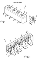
- the known from the prior art contact carrier 1 has a contact carrier housing 2, in which four contact openings 3 are provided. From a bottom of the contact carrier 1, not shown, the contact carrier openings 3 are each equipped with a dual spring contact 4, which is shown separately next to the contact carrier housing 2.
- This dual-spring contact 4 has two resilient legs 5, each having a connection portion 6 for forming a solder tab and contact springs 7 for receiving a mating connector, not shown. As an example, the connecting lugs 6 can be seen at a lower edge 8 of the contact carrier housing 2.
- the dual-spring contact 4 according to the prior art is integrally formed, wherein it is punched out for the production of a flat piece of sheet metal and a bend must be made in several directions in space.
- the in Fig. 2 illustrated erfindunumblee contact carrier 1 is provided with two-part dual-spring contacts, which are each formed by two resilient legs 5, which are fixed opposite in the contact carrier housing 2.
- To fix the springs in the legs 5 are each provided with a locking groove 9 and a latch 10 on each side.
- An inventive dual-spring contact 4 is in the in Fig. 3 shown second view of a contact carrier 1 according to the invention shown separately.
- the two resilient legs 5 of the dual-spring contact 4 are two separate components. This offers the advantage that a resistance between the connection tabs 6 can provide information as to whether a mating connector, not shown, is inserted or whether a contact resistance with an inserted mating connector changes and / or is outside predetermined tolerances.
- a contact dome 12 is embossed in the contact spring sections 11.
- a substantially point-shaped contact with a defined contact surface is made to a mating connector, not shown.
- a spring force between the opposite contact spring portions 11 can be adjusted by a corresponding bending of the resilient legs 5. Due to the two-part design of the dual-spring contact 4, this is possible in a particularly simple manner before assembly or before insertion into the contact carrier housing 2.
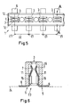
- a contact carrier 1 is simplified with a component 13 according to the invention, which is in Fig. 4 is shown.
- This has a strip-shaped carrier element 14 as well as four component elements 15 extending therefrom, each of which has a terminal strap section 16 and a contact spring section 11.
- These two sections 11, 16 are used to form the in Fig. 3 illustrated terminal lugs 6 and the contact spring portions 11 provided.
- a contact dome 12 is formed in the component 13 in the individual contact spring sections 11. This contact dome 12 is preferably formed at the same time in a punching of the component 13 from a band-shaped plate 17 shown in dashed lines.
- the component 13 with the component elements 15 is inserted from a rear side or underside of the contact carrier housing 2 into the housing such that the component elements 15 extend into the contact openings provided in the housing. Subsequently, the component 13 is angled to form the solder tabs and that substantially at an angle of 90 °. Subsequently, the carrier element 14 is separated along the dividing line 18 shown in broken lines from the component elements 15. In an alternative embodiment, the bending can also take place after the separation.
- two components 13 may be provided in the band-shaped plate 17, which are arranged to each other so that component elements of a second component, not shown, engage in the gaps 19 of the first component 13.
- the component 13 is in an embodiment not shown substantially longer than the provided with only four component elements 15 component 13 and is for example a band-shaped structure with a length of for example several meters, which can be wound onto a roll.
- circular spacer marks 20 are arranged in the carrier element 14, which provide precise control of advancement of the carrier element or precise positioning of the carrier element in a Abtrennvorgang to separate the desired number of component elements 15 allows.
- These distance marks 20 are arranged as well as the component elements 15 at a defined distance, as shown in the Fig. 5 is explained more clearly.
- the contact carrier 1 shown in a plan view is provided with four contact openings 3, the center lines 21 each having a defined grid spacing 22 from each other. Accordingly, the contact springs 7 are aligned with their contact points 12 each centered with respect to the respective center line 21. This ensures that the terminal lugs 6 are also aligned exactly in the defined grid spacing 22 to each other.
- FIG. 6 A detail view along the section line AA in Fig. 5 is in the Fig. 6 shown.
- the two resilient legs 5 are inserted from a bottom 23 in the contact carrier housing 2, so that the contact spring portions 11 extend with the contact springs 7 from the bottom 23 into the contact opening 3.
- the connecting lugs 6 are formed by bending the resilient legs 5, wherein the connecting lugs 6 are precisely aligned to a connecting plane 24 shown in dashed lines. Such a precise alignment is achieved, in particular, when the component elements 15 are angled together prior to the separation of the carrier elements and thereby aligned with each other.
Landscapes
- Engineering & Computer Science (AREA)
- Manufacturing & Machinery (AREA)
- Packaging Frangible Articles (AREA)
- Manufacturing Of Electrical Connectors (AREA)
- Coupling Device And Connection With Printed Circuit (AREA)
Applications Claiming Priority (1)
| Application Number | Priority Date | Filing Date | Title |
|---|---|---|---|
| DE102006057368 | 2006-12-04 |
Publications (2)
| Publication Number | Publication Date |
|---|---|
| EP1930987A2 true EP1930987A2 (fr) | 2008-06-11 |
| EP1930987A3 EP1930987A3 (fr) | 2009-05-06 |
Family
ID=39126187
Family Applications (1)
| Application Number | Title | Priority Date | Filing Date |
|---|---|---|---|
| EP07023394A Withdrawn EP1930987A3 (fr) | 2006-12-04 | 2007-12-04 | Support de contact à contact élastique |
Country Status (1)
| Country | Link |
|---|---|
| EP (1) | EP1930987A3 (fr) |
Cited By (8)
| Publication number | Priority date | Publication date | Assignee | Title |
|---|---|---|---|---|
| EP2164137A1 (fr) * | 2008-09-11 | 2010-03-17 | Sumitomo Wiring Systems, Ltd. | Connecteur de joint, terminal de joint, faisceau de câbles avec un connecteur de joint et son procédé d'assemblage |
| CN101997203A (zh) * | 2010-11-24 | 2011-03-30 | 中航光电科技股份有限公司 | 用于矩形电连接器的功率接触件 |
| WO2012058807A1 (fr) | 2010-11-03 | 2012-05-10 | Harting Electronics Gmbh & Co. Kg | Élément de contact pour douille de connecteur enfichable |
| EP2950397A1 (fr) * | 2013-05-24 | 2015-12-02 | Iriso Electronics Co., Ltd. | Connecteur |
| DE102015225159A1 (de) * | 2015-12-14 | 2017-06-14 | Continental Automotive Gmbh | Magnetfeldsensor mit einem Steckersockel |
| LU500674B1 (de) | 2021-09-21 | 2023-03-21 | Phoenix Contact Gmbh & Co | Elektrisches Kontaktelement |
| DE102021124327A1 (de) | 2021-09-21 | 2023-03-23 | Phoenix Contact Gmbh & Co. Kg | Elektrisches Kontaktelement |
| DE102021120385B4 (de) | 2020-08-10 | 2024-05-29 | Lear Corporation | Oberflächenmontagetechnik-Anschluss-Header, On-Board-Ladegerät und Oberflächenmontagetechnik-Verfahren zum Bereitstellen einer elektrischen Verbindung zu einer Leiterplatte |
Family Cites Families (6)
| Publication number | Priority date | Publication date | Assignee | Title |
|---|---|---|---|---|
| JPS5811076B2 (ja) * | 1978-12-25 | 1983-03-01 | 株式会社エルコ インタ−ナシヨナル | 電気接続子組立体 |
| US5785556A (en) * | 1996-07-16 | 1998-07-28 | Molex Incorporated | Edge connector for a printed circuit board |
| US6261107B1 (en) * | 1998-01-16 | 2001-07-17 | Molex Incorporated | Surface mount connector having improved terminal structure |
| US20010000368A1 (en) * | 1998-04-02 | 2001-04-26 | Ward Terrence S. | Method of manufacturing electrical connector contacts |
| US6048221A (en) * | 1998-08-13 | 2000-04-11 | The Whitaker Corporation | Electrical connector with reduced contact footprint |
| JP2006260978A (ja) * | 2005-03-17 | 2006-09-28 | Sumitomo Wiring Syst Ltd | 連鎖端子 |
-
2007
- 2007-12-04 EP EP07023394A patent/EP1930987A3/fr not_active Withdrawn
Cited By (15)
| Publication number | Priority date | Publication date | Assignee | Title |
|---|---|---|---|---|
| EP2164137A1 (fr) * | 2008-09-11 | 2010-03-17 | Sumitomo Wiring Systems, Ltd. | Connecteur de joint, terminal de joint, faisceau de câbles avec un connecteur de joint et son procédé d'assemblage |
| US7883362B2 (en) | 2008-09-11 | 2011-02-08 | Sumitomo Wiring Systems, Ltd. | Joint connector, joint terminal and a wiring harness with a joint connector |
| WO2012058807A1 (fr) | 2010-11-03 | 2012-05-10 | Harting Electronics Gmbh & Co. Kg | Élément de contact pour douille de connecteur enfichable |
| US8926352B2 (en) | 2010-11-03 | 2015-01-06 | HARTING Electronics GmbH | Contact element for plug-in connector socket |
| CN101997203A (zh) * | 2010-11-24 | 2011-03-30 | 中航光电科技股份有限公司 | 用于矩形电连接器的功率接触件 |
| CN101997203B (zh) * | 2010-11-24 | 2013-03-27 | 中航光电科技股份有限公司 | 用于矩形电连接器的功率接触件 |
| EP2950397A1 (fr) * | 2013-05-24 | 2015-12-02 | Iriso Electronics Co., Ltd. | Connecteur |
| CN105322332A (zh) * | 2013-05-24 | 2016-02-10 | 意力速电子工业株式会社 | 连接器 |
| US9466907B2 (en) | 2013-05-24 | 2016-10-11 | Iriso Electronics Co., Ltd. | Connector |
| CN113488790A (zh) * | 2013-05-24 | 2021-10-08 | 意力速电子工业株式会社 | 连接器 |
| DE102015225159A1 (de) * | 2015-12-14 | 2017-06-14 | Continental Automotive Gmbh | Magnetfeldsensor mit einem Steckersockel |
| DE102021120385B4 (de) | 2020-08-10 | 2024-05-29 | Lear Corporation | Oberflächenmontagetechnik-Anschluss-Header, On-Board-Ladegerät und Oberflächenmontagetechnik-Verfahren zum Bereitstellen einer elektrischen Verbindung zu einer Leiterplatte |
| LU500674B1 (de) | 2021-09-21 | 2023-03-21 | Phoenix Contact Gmbh & Co | Elektrisches Kontaktelement |
| DE102021124327A1 (de) | 2021-09-21 | 2023-03-23 | Phoenix Contact Gmbh & Co. Kg | Elektrisches Kontaktelement |
| WO2023046550A1 (fr) | 2021-09-21 | 2023-03-30 | Phoenix Contact Gmbh & Co. Kg | Élément de contact électrique |
Also Published As
| Publication number | Publication date |
|---|---|
| EP1930987A3 (fr) | 2009-05-06 |
Similar Documents
| Publication | Publication Date | Title |
|---|---|---|
| DE69722392T2 (de) | Elektrischer verbinder zusammengesetzt aus scheibenartigen einzelteilen | |
| DE68917080T2 (de) | Elektrischer Verbinder für elektronische Gedächtniskarten, Verfahren der Verwirklichung eines derartigen Verbinders und Lese-Schreibvorrichtung mit diesem Verbinder. | |
| DE69118808T2 (de) | Elektrischer Steckverbinder und dessen Herstellungsverfahren | |
| DE69211742T2 (de) | Leiterplattensteckverbinder | |
| EP1930987A2 (fr) | Support de contact à contact élastique | |
| DE69326613T2 (de) | Kartenverbinder mit flacher rückseite | |
| EP3375048B1 (fr) | Contact à enficher | |
| DE112017001259B4 (de) | Tragschienenbaugruppe mit einem Bussystem und einem eine Leiterplatte aufweisenden Elektronikgerät | |
| DE102005021568A1 (de) | Leiterplatte mit Einpressanschluss | |
| DE102016108825B4 (de) | Klemmanordnung und Anschlussklemme | |
| DE102013107156B4 (de) | Leiterplattenverbinder | |
| DE602004009268T2 (de) | Verbinder | |
| DE3345435A1 (de) | Verbinder, insbesondere steckverbinder, und verfahren zu seiner herstellung | |
| DE2405464A1 (de) | Vielfachsteckverbinder zur herstellung mehrerer elektrischer verbindungen | |
| DE2345583A1 (de) | Elektrische steckerleiste und verfahren zu ihrer herstellung | |
| EP0645856B1 (fr) | Procédé pour la fabrication d'un groupe d'éléments-contact pour un connecteur | |
| DE9415087U1 (de) | Steckbare elektrische Verbindungsvorrichtung | |
| EP3201994A1 (fr) | Barrette à broches | |
| DE102007044857A1 (de) | Verbindungselement | |
| DE102011089020B4 (de) | Kontaktverbinder und Verfahren zur Herstellung eines Kontaktverbinders | |
| WO2015132062A1 (fr) | Ensemble de raccordement, procédé de production d'un ensemble de raccordement et appareil électrique comprenant un ensemble de raccordement | |
| DE102013219979A1 (de) | Elektrische Verbindungsanordnung an einem Schaltungsträger, Verfahren zum Herstellen der Verbindungsanordnung und Steuergerät mit einer Verbindungsanordnung | |
| DE102012011047B4 (de) | Verbindungsbauteil und Schaltungsanordnung mit dem Verbindungsbauteil | |
| DE102019134369B4 (de) | Leadframe für Drahtbauteile mit Kulissenstruktur | |
| DE102007034389B4 (de) | Mehrpoliger elektrischer Steckverbinder |
Legal Events
| Date | Code | Title | Description |
|---|---|---|---|
| PUAI | Public reference made under article 153(3) epc to a published international application that has entered the european phase |
Free format text: ORIGINAL CODE: 0009012 |
|
| AK | Designated contracting states |
Kind code of ref document: A2 Designated state(s): AT BE BG CH CY CZ DE DK EE ES FI FR GB GR HU IE IS IT LI LT LU LV MC MT NL PL PT RO SE SI SK TR |
|
| AX | Request for extension of the european patent |
Extension state: AL BA HR MK RS |
|
| PUAL | Search report despatched |
Free format text: ORIGINAL CODE: 0009013 |
|
| AK | Designated contracting states |
Kind code of ref document: A3 Designated state(s): AT BE BG CH CY CZ DE DK EE ES FI FR GB GR HU IE IS IT LI LT LU LV MC MT NL PL PT RO SE SI SK TR |
|
| AX | Request for extension of the european patent |
Extension state: AL BA HR MK RS |
|
| RIC1 | Information provided on ipc code assigned before grant |
Ipc: H01R 43/16 20060101ALI20090330BHEP Ipc: H01R 13/11 20060101ALI20090330BHEP Ipc: H01R 12/22 20060101ALI20090330BHEP Ipc: H01R 12/36 20060101AFI20090330BHEP |
|
| 17P | Request for examination filed |
Effective date: 20091105 |
|
| AKX | Designation fees paid |
Designated state(s): AT BE BG CH CY CZ DE DK EE ES FI FR GB GR HU IE IS IT LI LT LU LV MC MT NL PL PT RO SE SI SK TR |
|
| 17Q | First examination report despatched |
Effective date: 20091221 |
|
| STAA | Information on the status of an ep patent application or granted ep patent |
Free format text: STATUS: THE APPLICATION IS DEEMED TO BE WITHDRAWN |
|
| 18D | Application deemed to be withdrawn |
Effective date: 20100706 |