EP1932236B1 - Regulation du cycle de service d'un regulateur de commutation en mode operationnel en frequence fixe - Google Patents
Regulation du cycle de service d'un regulateur de commutation en mode operationnel en frequence fixe Download PDFInfo
- Publication number
- EP1932236B1 EP1932236B1 EP06800924.0A EP06800924A EP1932236B1 EP 1932236 B1 EP1932236 B1 EP 1932236B1 EP 06800924 A EP06800924 A EP 06800924A EP 1932236 B1 EP1932236 B1 EP 1932236B1
- Authority
- EP
- European Patent Office
- Prior art keywords
- switch
- time
- regulator
- clock
- duty cycle
- Prior art date
- Legal status (The legal status is an assumption and is not a legal conclusion. Google has not performed a legal analysis and makes no representation as to the accuracy of the status listed.)
- Not-in-force
Links
- 239000003990 capacitor Substances 0.000 claims description 34
- 238000000034 method Methods 0.000 claims description 14
- 238000007599 discharging Methods 0.000 claims description 10
- 238000010586 diagram Methods 0.000 description 10
- 238000013459 approach Methods 0.000 description 8
- 230000004044 response Effects 0.000 description 5
- 230000009467 reduction Effects 0.000 description 4
- 230000007423 decrease Effects 0.000 description 3
- 238000004804 winding Methods 0.000 description 3
- 230000003213 activating effect Effects 0.000 description 2
- 230000033228 biological regulation Effects 0.000 description 2
- 230000008859 change Effects 0.000 description 2
- 230000003247 decreasing effect Effects 0.000 description 2
- 230000008569 process Effects 0.000 description 2
- 230000001419 dependent effect Effects 0.000 description 1
- 230000009977 dual effect Effects 0.000 description 1
- 238000012986 modification Methods 0.000 description 1
- 230000004048 modification Effects 0.000 description 1
Images




Classifications
-
- H—ELECTRICITY
- H03—ELECTRONIC CIRCUITRY
- H03K—PULSE TECHNIQUE
- H03K7/00—Modulating pulses with a continuously-variable modulating signal
- H03K7/08—Duration or width modulation ; Duty cycle modulation
-
- H—ELECTRICITY
- H02—GENERATION; CONVERSION OR DISTRIBUTION OF ELECTRIC POWER
- H02M—APPARATUS FOR CONVERSION BETWEEN AC AND AC, BETWEEN AC AND DC, OR BETWEEN DC AND DC, AND FOR USE WITH MAINS OR SIMILAR POWER SUPPLY SYSTEMS; CONVERSION OF DC OR AC INPUT POWER INTO SURGE OUTPUT POWER; CONTROL OR REGULATION THEREOF
- H02M3/00—Conversion of DC power input into DC power output
- H02M3/02—Conversion of DC power input into DC power output without intermediate conversion into AC
- H02M3/04—Conversion of DC power input into DC power output without intermediate conversion into AC by static converters
- H02M3/10—Conversion of DC power input into DC power output without intermediate conversion into AC by static converters using discharge tubes with control electrode or semiconductor devices with control electrode
- H02M3/145—Conversion of DC power input into DC power output without intermediate conversion into AC by static converters using discharge tubes with control electrode or semiconductor devices with control electrode using devices of a triode or transistor type requiring continuous application of a control signal
- H02M3/155—Conversion of DC power input into DC power output without intermediate conversion into AC by static converters using discharge tubes with control electrode or semiconductor devices with control electrode using devices of a triode or transistor type requiring continuous application of a control signal using semiconductor devices only
- H02M3/156—Conversion of DC power input into DC power output without intermediate conversion into AC by static converters using discharge tubes with control electrode or semiconductor devices with control electrode using devices of a triode or transistor type requiring continuous application of a control signal using semiconductor devices only with automatic control of output voltage or current, e.g. switching regulators
-
- H—ELECTRICITY
- H03—ELECTRONIC CIRCUITRY
- H03K—PULSE TECHNIQUE
- H03K4/00—Generating pulses having essentially a finite slope or stepped portions
- H03K4/06—Generating pulses having essentially a finite slope or stepped portions having triangular shape
- H03K4/08—Generating pulses having essentially a finite slope or stepped portions having triangular shape having sawtooth shape
- H03K4/48—Generating pulses having essentially a finite slope or stepped portions having triangular shape having sawtooth shape using as active elements semiconductor devices
- H03K4/50—Generating pulses having essentially a finite slope or stepped portions having triangular shape having sawtooth shape using as active elements semiconductor devices in which a sawtooth voltage is produced across a capacitor
Definitions
- This invention relates to voltage regulators.
- this invention relates to switch-mode voltage regulators.
- Switch-mode regulators or switching regulators as they are commonly known, are typically used as voltage regulators because they exhibit higher efficiency than an equivalent linear regulator circuit at heavy loads.
- a typical switching regulator operates by repeatedly turning a power switch fully on and then fully off, generating a pulse-width modulated signal that is averaged to the final voltage with an inductor.
- the switching power supply is of the type having a transformer having primary and secondary windings for generating an output voltage at the secondary winding, a power switch for driving the primary winding, and controller circuitry for activating the power switch.
- the controller circuitry includes an oscillator and frequency shift means, wherein the oscillator generates PWM pulses having a predetermined frequency for use in activating the power switch.
- the frequency shift means gradually shifts the frequency of the PWM pulses at a shift rate in response to the output voltage decreasing to below a threshold level.
- Document US 6262542 discloses an electronic ballast for use in illuminating a lamp includes a lamp driving circuit having a pulse-width modulated signal generator, a timing capacitor coupled to the lamp driving circuit, and a power controller.
- the power controller uses a current sense resistor to detect a current flowing through the lamp and an operational amplifier circuit to compare a signal associated with the detected current to a reference voltage associated with a desired lamp current. Based on the comparison, the power controller provides a correction current to the timing capacitor to control a duty cycle of an output of the pulse-width modulated signal generator.
- Document US 5710697 discloses a power supply controller implementing frequency foldback and volt-second duty cycle clamp features.
- An oscillator timing capacitor is charged with a fixed current and is discharged with a fixed current when the output voltage is above a predetermined level and with a decreasing current when the output voltage falls below the predetermined level, so as to decrease the power supply operating frequency during short circuit or overload fault conditions.
- a volt-second duty cycle clamp circuit limits the duty cycle to a maximum value which is independent of the tolerance of a capacitor which sets the maximum duty cycle as a function of the power supply input voltage.
- Document US 6198265 discloses an electrical circuit provides a fixed frequency switching regulator, having improved dynamic response, and a low count of external discrete elements.
- a current source is used to charge a timing capacitor.
- a comparator is used in conjunction with a hysteresis circuit so that as the timing capacitor is charged the voltage on one input of the comparator rises until reaching a set input voltage level whereupon the timing capacitor is discharged to ground.
- a PWM latch logic element is used to control output to a control switch, a FET, so that positive going output pulses are received at an output terminal.
- a divider network between the output terminal and the timing capacitor along with a switch controlled by the PWM latch element are used for slope compensation for maintaining operational synchronization to the oscillator.
- Document US 6366070 discloses a switching voltage regulator employs a dual modulation scheme to control the regulator's switching components.
- a control circuit indirectly monitors load current. When the load decreases, the control circuit reduces both the duty ratio and the frequency of the control signals which operate the switching transistors, thereby maintaining a high efficiency level over a wider output current range than can be achieved with fixed-frequency control signals.
- the present invention is particularly described in a step-down converter embodiment. Nevertheless, the invention is not limited to this particular embodiment and, in fact, may be implemented on any suitable switching regulator.
- the basic invention, as well as alternative implementations of the invention, will be discussed in more detail below.
- FIG. 1 shows a basic, conventional switching regulator system 100.
- FIG. 1 includes an oscillated clock 102 of a pulse-width modulated (PWM) system, an inverter 104, a flip-flop 106, a switch 108, an inductor 110, a current source 112, an output capacitor 114, a resistor divider 116 and 118, a voltage feedback amplifier 120 (or any suitable amplifier), a feedback capacitor 122, and a current comparator 124 (or any other suitable comparator).
- PWM pulse-width modulated
- inverter 104 preferably causes the PWM switch to turn ON coincident with the end of the ON cycle of clock 102. At least in this respect, the clock and the PWM switch are preferably out of phase with one another.
- the switching regulator As the input voltage of the power supply system becomes smaller -- e.g., when a battery's voltage drops as a result of usage of the battery --, the switching regulator is forced to operate at a very high clock cycle rate to maintain a substantially constant VOUT. As the clock cycle rate increases, and, consequently, the clock cycle time decreases, it becomes difficult to achieve a very high and/or a very low switch-ON duty cycle as operating conditions may at times require.
- FIG. 2A and 2B show clock-oscillated signals generated by the clock 102 of PWM system 100 shown in FIG. 1 .
- FIG. 3 shows a conventional clock oscillator 300 of the PWM system shown in FIG. 1 .
- Clock oscillator includes a charging current source 302, an oscillating capacitor 304, a first comparator 306, a switch 308, a discharging current sink 310, and a second comparator 312. Also indicated are Vramp and VN (which is compared to Vramp using comparator 306 for opening and closing switch 308).
- the most common method of generating constant repeating switching clock cycles for the clock oscillator 300 of the PWM system is by charging oscillator capacitor 304 with a current using charging source 302 until the capacitor voltage is charged up to the preset level VTH (Voltage Threshold High) and resetting the oscillator to VTL (Voltage Threshold Low) after the capacitor reaches VTH.
- VTH Voltage Threshold High
- VTL Voltage Threshold Low
- T 1 Cosc Icharge ⁇ VTH
- T 2 Cosc Idischarge ⁇ VTH
- this oscillator reset process takes a fraction of the total clock cycle time.
- the switching cycle of the PWM switch 108 begins when switch 308 turns ON at the beginning of Tl (see FIGs. 2A, 2B and 3 ).
- the switch-ON duration is determined by the duty cycle which is a function of VIN and VOUT of PWM switching regulator 300, as described above.
- the switch-ON duration may end at any time during T1. If switch 108 has not been switched OFF by the beginning of T2 and switch 308 is not allowed to turn ON longer than one clock cycle (no cycle skipping) then, switch 308 is typically forced to turn OFF at the beginning of T2 when the oscillator resets.
- T2 is usually determined by the power transistor switch 108 (see FIG. 1 ) turn-OFF/ON time.
- Typical maximum duty cycle with no cycle skipping ranges from 90% to 95%.
- VIN/VOUT condition of the PWM regulator requires a duty cycle that is higher than the oscillator maximum duty cycle can provide, the output loses regulation. This condition may occur, for example, when a step down converter has a VIN (Input Voltage) that is very close to VOUT (Output Voltage).
- cycle skipping is as follows: a 10 microsecond clock cycle time with OFF time T2 of 1 microsecond and maximum ON time Tl of 9 microsecond gives maximum duty cycle of 90%. If the regulator operation requires a 91% duty cycle, then it follows there will be one non-reset cycle with 10 microseconds ON time for every 9 reset cycles at T2 with 9 microseconds ON time each. This one cycle skip in every 10 cycles on the average has duty cycle of 91%.
- Another prior art method uses an open loop comparator approach.
- the system remains in the oscillator-based constant frequency PWM mode until the OFF time reaches the preset level.
- the system then switches to the fixed off time variable frequency mode with no oscillator involved.
- the disadvantage of this is that a frequency hysteresis is needed to switch back to the other mode when the duty cycle reduces and the abrupt mode change sometimes cause system frequency instability.
- the pulse-width-modulated voltage regulator preferably includes a clock oscillator.
- the clock oscillator has a capacitor.
- the oscillator provides a clock signal.
- the method includes using a charging current to charge the capacitor for a charging period of time, using a discharging current to discharge the capacitor for a discharging period of time, and, when desired, extending the charging period of time by diverting a portion of the charging current.
- the preferred embodiment of the invention preferably provides systems and methods for operating the switch at a duty cycle of higher than 90% (or some other suitable, preferably predetermined, duty cycle ratio).
- the preferred embodiment of the invention can obtain these higher duty cycles in a voltage regulator similar to the exemplary regulator shown in FIG. 1 without cycle skipping.
- the circuit according to the invention preferably resets every switching cycle, as will be described, and incorporates an analog feedback loop within the clock oscillator system of the PWM system to extend duty cycle time by keeping switch-OFF time constant while increasing switch-ON time.
- the circuit sets a reference time of a duration T3, which is preferably slightly longer than T2 and compares the PWM switch OFF time, Toff, with T3.
- T3 a duration of a duration
- the clock oscillator PWM switch turns ON until it is forced to turn OFF during T2 which is shorter than the reference T3.
- an analog feedback loop closes as follows.
- the analog feedback loop preferably includes a high-gain negative feedback amplifier that forces the switch OFF time, Toff, of the PWM switch to be the same time duration as the reference T3 by reducing the oscillator charging current Icharge. This extends the total time of the duty cycle.
- the invention preferably adjusts the clock cycle time by increasing the T1 of the clock cycle. This allows for an increase in the PWM switch ON time which can then provide the required duty cycle.
- FIG. 4-8 show the invention in detail.
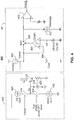
- FIG. 4 shows a schematic diagram of one embodiment of a clock oscillator system 400 including an oscillator circuit 401 and loop amplifier circuit 402 according to the invention.
- Oscillator circuit 401 corresponds to oscillator 300 shown in FIG. 3 .
- Amplifier 401 preferably includes switches 414 and 416, which switch ON (close) and switch OFF (open) in response to signals received from Vclock and Toff (PWM switch OFF time), respectively, amplifier capacitor 418, current sources 420 and 422, transistor 424, and resistor 426. Resistor 426 preferably adjusts the amount of current that transistor 424 conducts.
- amplifier 402 of the circuit according to the invention is implemented as a charge pump charging amplifier capacitor 418 which serves as the loop filter for loop response speed control by amplifier 402 of oscillator circuit 400.
- Iup from current source 420
- Idown flows out of amplifier capacitor 418 to discharge amplifier capacitor 418.
- the Up charge Iup ⁇ switch 414 ON time
- the Down charge Idown ⁇ switch 416 ON time
- Vx voltage potential associated with amplifier capacitor 4108 rises preferably only when the up charge is higher than the down charge. And when Vx rises to above transistor 424 turn-ON threshold, transistor 424 then starts conducting and takes the oscillator capacitor charging current Icharge (provided by source 402) away from oscillator capacitor 404. This extends the clock cycle ON time, Ti.
- the clock cycle ON time extension is illustrated in greater detail in the following example.
- amplifier 401 extends clock cycle ON time, and, thereby, can increase the effective duty cycle without cycle skipping:
- Switch 414 is controlled by Vclock as shown coming out from comparator 412.
- Vclock provides a T1 period and a constant T2 of 1 microsecond.
- Switch 416 is controlled by the PWM system switch OFF time Toff.
- Vx remains low when Toff is longer then 1.3 microsecond. This condition corresponds to an 87% duty cycle or lower in a 10 microsecond total clock cycle.
- Toff When the system requires duty cycle higher than 87%, Toff will be pushed shorter than 1.3 microseconds. Under this condition the Up charge is more than the Down charge and Vx will rise to turn transistor 424 ON and the loop closes to take Icharge, which charges oscillator capacitor 404, away from oscillator circuit 401.
- the clock cycle ON time, T1 is extended to satisfy the longer duty cycle required by the PWM system and the Toff is forced back up to 1.3 microseconds by the negative feedback amplifier. It should be noted that the clock cycle ON time, T1, is extended without extending the clock cycle OFF time, T2, thereby effectively allowing the PWM to have a higher duty cycle.
- the pulse-width-modulated system automatically adjusts the amount of the cycle extension time.
- this analog-feedback-loop-controlled approach is preferably always oscillator-controlled switching with no abrupt or sudden mode change as in the case of one of the prior art approaches.
- the invention circuit can also be modified to fix the PWM switch-ON time while extending the duty cycle time.
- This approach preferably achieves a fixed frequency (no cycle skipping) very low duty cycle PWM operation to avoid similar cycle-skipping audible noise -- e.g., when cycles are skipped and the voltage regulator does not turn ON such as in light output load conditions.
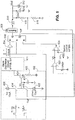
- FIG. 5 shows a schematic diagram of a switching regulator system 500 that incorporates the circuit according to the invention for at least the purpose of extending the ON duty cycle of the PWM.
- the circuit shown in FIG. 5 may preferably implements oscillator circuit 401 and the amplifier 401 of FIG. 4 in a voltage regulator such as the conventional regulator 100 shown in FIG. 1 . Therefore, elements 504, 506, 508, 510, 512, 514, 516, 518, 520, 522, and 524 are similar to the corresponding elements in FIG. 1 .
- Toff is derived from the inverse of the PWM switch ON signal.
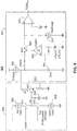
- FIG. 6 is a schematic diagram of an amplifier circuit 602 according to the invention that is used for duty cycle reduction.
- each of the elements 601, 602, 603, 604, 608, 610, 612, 614, 616, 618, 620, 622, 624, and 626 all preferably correspond to the similar elements shown in FIG. 4 .
- duty cycle reduction is preferably obtained by comparing Vclock with the PWM switch-ON time at switches 614 and 616, respectively, instead of PWM switch-OFF time.
- amplifier 602 preferably maintains the PWM switch-ON time (instead of the switch-OFF time) at 1.3 microseconds (or other suitable time period). By limiting PWM switch-ON time in this fashion, the duty cycle is reduced and can be maintained at a relatively low level.
- FIG. 7 shows a schematic diagram of a switching regulator system 700 that incorporates the invention circuit to achieve lower duty cycle (reduce the ON duty cycle of the PWM regulator).
- Switching regulator system 700 incorporates oscillator 600 and amplifier 601 according to the invention in a way that limits the ON duty cycle of the PWM.
- the circuit shown in FIG. 7 preferably combines the conventional regulator shown in FIG. 1 with the clock oscillator 600 and the amplifier 601 of FIG. 6 .
- the circuit in FIG. 7 operates as follows:
- Switch 614 is controlled by Vclock as shown coming out from comparator 612 (shown in FIG. 6 ).
- Vclock provides a T1 period and a constant T2 of 1 microsecond.
- Switch 616 is controlled by the PWM system switch ON time Ton.
- Vx remains low when Ton is longer then 1.3 microsecond. This condition corresponds to any duty cycle except a relatively small duty cycle.
- Ton When the system requires such a relatively low duty cycle, Ton will be pushed shorter than 1.3 microseconds. Under this condition the Up charge is more than the Down charge and Vx will rise to turn transistor 624 ON and the loop closes to take Icharge, which charges oscillator capacitor 604 (not shown in FIG. 7 ), away from oscillator circuit 600.
- FIG. 8 is a schematic diagram of a clock oscillator system 800 for both duty cycle extension and reduction.
- the circuit includes clock oscillator 801 and amplifier 802.
- Elements 801, 802, 804, 806, 808, 810, 812, 814, 818, 820, 824 and 826 are essentially the same as the corresponding elements shown in FIGs. 4 and 6 .
- the additional functionality of FIG. 8 is added by additional logic and an additional switch 817.
- Additional logic includes AND gates 824 and 826 as well as inverters 828 and 830.
- Switch 816 is preferably controlled by the PWM switch ON time Ton and switch 817 is preferably controlled by the PWM switch OFF time Toff (through inverter 828).
- PWM switch ON time Ton When the duty cycle is higher than 50%, AND gate 826 allows switch 817 to turn ON and AND gate 824 disables switch 816 for duty cycle extension.
- Duty cycle extension is obtained because the operation of amplifier 801 is balanced using the switch OFF time of the PWM switch (not shown) similar to the circuit shown in FIG 5 .
- AND gate 826 disables switch 817 and AND gate 824 turns switch 816.
- Duty cycle reduction is obtained because the operation of amplifier 802 is balanced using the switch ON time of the PWM switch (not shown) similar to the circuit shown in FIG. 7 .
Landscapes
- Engineering & Computer Science (AREA)
- Power Engineering (AREA)
- Dc-Dc Converters (AREA)
Claims (9)
- Système d'oscillateur d'horloge (400) qui est configuré pour fournir un signal d'horloge (Vclock) à une opération de commande d'un régulateur de commutation incluant un commutateur de régulateur (508), le système d'oscillateur d'horloge comprenant :- un circuit d'oscillateur (401) comprenant :un condensateur (404) ;une source de courant (403) qui est configurée pour utiliser un courant de chargement pendant une période de temps de chargement pour charger le condensateur (404) ; etun dissipateur de courant (410) qui est configuré pour utiliser un courant de déchargement pendant une période de temps de déchargement pour décharger le condensateur (404) ; etcaractérisé par- un circuit d'amplificateur (402) qui est configuré pour prolonger la période de temps de chargement en déviant une portion du courant de chargement, le circuit d'amplificateur (402) incluant un premier commutateur (414) commandé par le signal d'horloge (Vclock) et un deuxième commutateur (416) commandé par une durée éteinte du commutateur de régulateur (508) pour comparer le signal d'horloge (Vclock) au niveau du premier commutateur (414) à la durée éteinte du commutateur de régulateur (508) au niveau du deuxième commutateur (416), etdévier la portion du courant de chargement en fonction de la comparaison du signal d'horloge (Vclock) et de la durée éteinte du commutateur de régulateur (508).
- Système d'oscillateur d'horloge (400) selon la revendication 1, dans lequel le système d'oscillateur d'horloge (400) est configuré pour maintenir la période de temps de déchargement constante indépendamment du fait que le circuit d'amplificateur (402) prolonge la période de temps de chargement.
- Système d'oscillateur d'horloge (400) selon la revendication 1, dans lequel le système d'oscillateur d'horloge (400) fournit un signal d'horloge pour un régulateur de commutation à modulation d'impulsions en durée.
- Système d'oscillateur d'horloge (400) selon la revendication 1, dans lequel l'amplificateur (402) comprend en outre une entrée depuis une sortie du circuit d'oscillateur (401).
- Système d'oscillateur d'horloge (800) selon l'une quelconque des revendications précédentes, dans lequel le circuit d'amplificateur comprend en outre un troisième commutateur (816) commandé par une durée allumée du commutateur de régulateur ; et
dans lequel le deuxième commutateur (817) est autorisé à s'allumer et le troisième commutateur (816) est désactivé pour comparer le signal d'horloge (Vclock) au niveau du premier commutateur (814) à la durée éteinte du commutateur de régulateur au niveau du deuxième commutateur (817) lorsqu'un cycle de service du régulateur de commutation est supérieur à 50 % ;
dans lequel le deuxième commutateur (817) est désactivé et le troisième commutateur (816) est autorisé à s'allumer pour comparer le signal d'horloge (Vclock) au niveau du premier commutateur (814) à la durée allumée du commutateur de régulateur au niveau du troisième commutateur (816) lorsque le cycle de service du régulateur de commutation est inférieur à 50 % ; et
dévier la portion du courant de chargement se base sur la comparaison du signal d'horloge (Vclock) à la durée allumée du commutateur de régulateur ou la durée éteinte du commutateur de régulateur, respectivement. - Procédé d'augmentation du cycle de service dans un régulateur de tension à modulation d'impulsions en durée, le régulateur de tension à modulation d'impulsions en durée incluant un commutateur (508) et un oscillateur d'horloge (401) ayant un condensateur (404), l'oscillateur (401) étant configuré pour fournir un signal d'horloge (Vclock) pour opérer le régulateur de tension, le procédé comprenant :utiliser un courant de chargement pour charger le condensateur (404) pendant une période de temps de chargement ;utiliser un courant de déchargement pour décharger le condensateur (404) pendant une période de temps de déchargement ; etcaractérisé par les étapes consistant àcommander un premier commutateur (414) par le signal d'horloge (Vclock) ;commander un deuxième commutateur (416) par une durée éteinte du commutateur (508) ; etcomparer le signal d'horloge (Vclock) au niveau du premier commutateur (414) à la durée éteinte du commutateur (508) au niveau du deuxième commutateur (416) pour prolonger la période de temps de chargement en déviant une portion du courant de chargement en fonction de la comparaison du signal d'horloge (Vclock) et de la durée éteinte du commutateur (508).
- Procédé selon la revendication 6, comprenant en outre maintenir la période de temps de déchargement constante indépendamment du fait que le circuit d'amplificateur (802) prolonge la période de temps de chargement.
- Procédé selon la revendication 6, comprenant en outre utiliser l'oscillateur d'horloge (401) pour fournir un signal d'horloge pour le régulateur de commutation à modulation d'impulsions en durée.
- Procédé selon la revendication 6, comprenant en outre utiliser une sortie du système d'oscillateur d'horloge comme entrée vers le système d'oscillateur d'horloge.
Priority Applications (1)
| Application Number | Priority Date | Filing Date | Title |
|---|---|---|---|
| EP12000109.4A EP2445096B1 (fr) | 2005-10-03 | 2006-08-07 | Contrôle de facteur d'utilisation à régulateur de commutation dans un fonctionnement de fréquence fixe |
Applications Claiming Priority (2)
| Application Number | Priority Date | Filing Date | Title |
|---|---|---|---|
| US11/242,095 US7388444B2 (en) | 2005-10-03 | 2005-10-03 | Switching regulator duty cycle control in a fixed frequency operation |
| PCT/US2006/030798 WO2007040814A1 (fr) | 2005-10-03 | 2006-08-07 | Regulation du cycle de service d'un regulateur de commutation en mode operationnel en frequence fixe |
Related Child Applications (2)
| Application Number | Title | Priority Date | Filing Date |
|---|---|---|---|
| EP12000109.4A Division EP2445096B1 (fr) | 2005-10-03 | 2006-08-07 | Contrôle de facteur d'utilisation à régulateur de commutation dans un fonctionnement de fréquence fixe |
| EP12000109.4A Division-Into EP2445096B1 (fr) | 2005-10-03 | 2006-08-07 | Contrôle de facteur d'utilisation à régulateur de commutation dans un fonctionnement de fréquence fixe |
Publications (2)
| Publication Number | Publication Date |
|---|---|
| EP1932236A1 EP1932236A1 (fr) | 2008-06-18 |
| EP1932236B1 true EP1932236B1 (fr) | 2017-02-22 |
Family
ID=37497029
Family Applications (2)
| Application Number | Title | Priority Date | Filing Date |
|---|---|---|---|
| EP06800924.0A Not-in-force EP1932236B1 (fr) | 2005-10-03 | 2006-08-07 | Regulation du cycle de service d'un regulateur de commutation en mode operationnel en frequence fixe |
| EP12000109.4A Not-in-force EP2445096B1 (fr) | 2005-10-03 | 2006-08-07 | Contrôle de facteur d'utilisation à régulateur de commutation dans un fonctionnement de fréquence fixe |
Family Applications After (1)
| Application Number | Title | Priority Date | Filing Date |
|---|---|---|---|
| EP12000109.4A Not-in-force EP2445096B1 (fr) | 2005-10-03 | 2006-08-07 | Contrôle de facteur d'utilisation à régulateur de commutation dans un fonctionnement de fréquence fixe |
Country Status (5)
| Country | Link |
|---|---|
| US (1) | US7388444B2 (fr) |
| EP (2) | EP1932236B1 (fr) |
| JP (1) | JP5066526B2 (fr) |
| KR (1) | KR101332677B1 (fr) |
| WO (1) | WO2007040814A1 (fr) |
Families Citing this family (20)
| Publication number | Priority date | Publication date | Assignee | Title |
|---|---|---|---|---|
| US8036762B1 (en) | 2007-05-09 | 2011-10-11 | Zilker Labs, Inc. | Adaptive compensation in digital power controllers |
| JP4971086B2 (ja) * | 2007-09-13 | 2012-07-11 | 株式会社リコー | スイッチングレギュレータ及びそのパルス幅制限値調整方法 |
| US9218769B2 (en) * | 2008-03-20 | 2015-12-22 | Apple Inc. | Anti-phase pulse width modulator |
| TWI377770B (en) * | 2009-03-17 | 2012-11-21 | Leadtrend Tech Corp | Frequency-jittering apparatuses, frequency-jittering methods and power management devices |
| CN102214986A (zh) * | 2010-04-06 | 2011-10-12 | 大连精拓光电有限公司 | 用于为开关电源变换器提供工作频率的系统 |
| US8536813B2 (en) | 2010-05-19 | 2013-09-17 | The Invention Science Fund I Llc | Motor with rotor-mounted control circuitry |
| US8754626B2 (en) * | 2010-06-18 | 2014-06-17 | Freescale Semiconductor, Inc. | Switching regulator with input current limiting capabilities |
| TWI407668B (zh) * | 2010-07-09 | 2013-09-01 | Leadtrend Tech Corp | 電源供應器以及抑制電源供應器之輸出電壓波動的方法 |
| CN101938214B (zh) * | 2010-07-09 | 2012-09-05 | 无锡市晶源微电子有限公司 | 具有自延时保护功能的内部振荡器模块 |
| US8294446B2 (en) | 2010-08-13 | 2012-10-23 | Semiconductor Components Industries, Llc | Switching regulator device and method with adaptive frequency foldback |
| JP5714924B2 (ja) * | 2011-01-28 | 2015-05-07 | ラピスセミコンダクタ株式会社 | 電圧識別装置及び時計制御装置 |
| US9293989B2 (en) * | 2011-04-21 | 2016-03-22 | Green Solution Technology Co., Ltd. | DC to DC buck converting controller with programmable on-time period unit |
| TWI481169B (zh) * | 2011-05-27 | 2015-04-11 | Leadtrend Tech Corp | 控制切換式電源轉換器之功率開關跨壓之方法及其電路 |
| TWI470918B (zh) * | 2012-12-17 | 2015-01-21 | Upi Semiconductor Corp | 直流對直流轉換器、時間產生電路及其操作方法 |
| US10141832B2 (en) * | 2015-07-10 | 2018-11-27 | Maxim Integrated Products, Inc. | Systems and methods for reducing switch stress in switched mode power supplies |
| US11014182B2 (en) * | 2015-07-17 | 2021-05-25 | Illinois Tool Works Inc. | Method and apparatus for providing welding type power |
| US9646657B2 (en) * | 2015-09-04 | 2017-05-09 | Intel Corporation | Power loss capacitor test using voltage ripple |
| KR102453665B1 (ko) | 2015-09-22 | 2022-10-12 | 삼성전자주식회사 | 선형성을 제고한 전압 레귤레이터 |
| CN108415502B (zh) * | 2018-03-28 | 2020-03-31 | 东南大学 | 一种无有限周期震荡的数字线性稳压电源及稳压方法 |
| EP4020815B1 (fr) * | 2020-12-28 | 2026-02-25 | STMicroelectronics S.r.l. | Circuit de décodeur de modulation de largeur d'impulsion, dispositif correspondant et procédés de fonctionnement |
Family Cites Families (28)
| Publication number | Priority date | Publication date | Assignee | Title |
|---|---|---|---|---|
| DE1638009B2 (de) * | 1968-01-23 | 1972-08-24 | Danfoss A/S, Nordborg (Danemark) | Gleichspannungsgespeiste, geregelte gleichspannungsversorgung |
| US3571697A (en) * | 1968-12-16 | 1971-03-23 | Collins Radio Co | Variable impedance switching regulator |
| US3579091A (en) * | 1969-05-16 | 1971-05-18 | Bell Telephone Labor Inc | Switching regulator with random noise generator |
| US3772588A (en) * | 1971-10-01 | 1973-11-13 | Cogar Corp | Dual control loop switching regulator |
| US3879647A (en) * | 1974-06-07 | 1975-04-22 | Bell Telephone Labor Inc | DC to DC converter with regulation having accelerated soft start into active control region of regulation and fast response overcurrent limiting features |
| US3978393A (en) * | 1975-04-21 | 1976-08-31 | Burroughs Corporation | High efficiency switching regulator |
| JPS58103221A (ja) * | 1981-12-15 | 1983-06-20 | Sony Corp | 可変発振器 |
| US4479174A (en) * | 1982-11-03 | 1984-10-23 | Reliance Electric Company | Efficiency increasing circuit for switching power supplies operating at low power levels |
| US4541041A (en) * | 1983-08-22 | 1985-09-10 | General Electric Company | Full load to no-load control for a voltage fed resonant inverter |
| US4578630A (en) * | 1984-11-23 | 1986-03-25 | At&T Bell Laboratories | Buck boost switching regulator with duty cycle limiting |
| US4634956A (en) * | 1985-01-10 | 1987-01-06 | Motorola, Inc. | DC to DC converter |
| US4672303A (en) * | 1986-08-28 | 1987-06-09 | International Business Machines Corporation | Inductor current control circuit |
| US4683529A (en) * | 1986-11-12 | 1987-07-28 | Zytec Corporation | Switching power supply with automatic power factor correction |
| US4819122A (en) * | 1987-04-02 | 1989-04-04 | Cherry Semiconductor Corporation | Over-current timer modulator |
| US4928200A (en) * | 1987-04-02 | 1990-05-22 | Cherry Semiconductor Corporation | Overcurrent protection for switching mode power converter |
| US4929882A (en) * | 1987-06-23 | 1990-05-29 | National Semiconductor Corporation | Apparatus for converting DC to DC having non-feed back variable hysteretic current-mode control for maintaining approximately constant frequency |
| US4814684A (en) * | 1987-09-30 | 1989-03-21 | Trw Inc. | Apparatus for extending the Vout/Vin ratio of a DC-to-DC converter |
| EP0689731A1 (fr) * | 1993-03-17 | 1996-01-03 | National Semiconductor Corporation | Circuit de glissemant de fréquence pour régulateur à découpage |
| US5481178A (en) * | 1993-03-23 | 1996-01-02 | Linear Technology Corporation | Control circuit and method for maintaining high efficiency over broad current ranges in a switching regulator circuit |
| DE4340924C2 (de) * | 1993-12-01 | 1995-10-05 | Telefunken Microelectron | Frequenzstabiler RC-Oszillator |
| AU1726795A (en) * | 1994-02-15 | 1995-08-29 | Rambus Inc. | Amplifier with active duty cycle correction |
| US5710697A (en) * | 1996-03-26 | 1998-01-20 | Unitrode Corporation | Power supply controller having frequency foldback and volt-second duty cycle clamp features |
| US5705919A (en) * | 1996-09-30 | 1998-01-06 | Linear Technology Corporation | Low drop-out switching regulator architecture |
| JPH10323024A (ja) * | 1997-05-19 | 1998-12-04 | Toshiba Corp | チョッパ装置の制御装置 |
| US6198265B1 (en) * | 1998-06-19 | 2001-03-06 | Unisem, Inc. | Fixed frequency switching regulator with improved dynamic response |
| KR100333974B1 (ko) * | 1999-05-19 | 2002-04-24 | 김덕중 | 전자식 안정기 |
| US6366070B1 (en) * | 2001-07-12 | 2002-04-02 | Analog Devices, Inc. | Switching voltage regulator with dual modulation control scheme |
| US6967514B2 (en) * | 2002-10-21 | 2005-11-22 | Rambus, Inc. | Method and apparatus for digital duty cycle adjustment |
-
2005
- 2005-10-03 US US11/242,095 patent/US7388444B2/en not_active Expired - Lifetime
-
2006
- 2006-08-07 EP EP06800924.0A patent/EP1932236B1/fr not_active Not-in-force
- 2006-08-07 KR KR1020087010700A patent/KR101332677B1/ko not_active Expired - Fee Related
- 2006-08-07 WO PCT/US2006/030798 patent/WO2007040814A1/fr not_active Ceased
- 2006-08-07 JP JP2008534524A patent/JP5066526B2/ja not_active Expired - Fee Related
- 2006-08-07 EP EP12000109.4A patent/EP2445096B1/fr not_active Not-in-force
Non-Patent Citations (1)
| Title |
|---|
| None * |
Also Published As
| Publication number | Publication date |
|---|---|
| WO2007040814A1 (fr) | 2007-04-12 |
| EP2445096A3 (fr) | 2013-10-16 |
| EP2445096B1 (fr) | 2016-07-13 |
| KR101332677B1 (ko) | 2013-11-25 |
| KR20080075496A (ko) | 2008-08-18 |
| JP5066526B2 (ja) | 2012-11-07 |
| US7388444B2 (en) | 2008-06-17 |
| JP2009510995A (ja) | 2009-03-12 |
| US20070075790A1 (en) | 2007-04-05 |
| EP2445096A2 (fr) | 2012-04-25 |
| EP1932236A1 (fr) | 2008-06-18 |
Similar Documents
| Publication | Publication Date | Title |
|---|---|---|
| EP2445096B1 (fr) | Contrôle de facteur d'utilisation à régulateur de commutation dans un fonctionnement de fréquence fixe | |
| US11563378B2 (en) | Seamless DCM-PFM transition for single pulse operation in DC-DC converters | |
| US8310216B2 (en) | Synchronous rectifier control for synchronous boost converter | |
| US8525502B2 (en) | Digital pulse-frequency modulation controller for switch-mode power supplies with frequency targeting and ultrasonic modes | |
| JP4291324B2 (ja) | Dc/dcコンバータのための制御装置 | |
| EP1969705B1 (fr) | Circuit generateur de compensation de pente d'un regulateur de commutation | |
| US8030910B2 (en) | DC-DC converter | |
| EP3641118B1 (fr) | Techniques de commande de régulateur aux charges légères | |
| US6674272B2 (en) | Current limiting technique for a switching power converter | |
| US7777469B2 (en) | Converter having PWM ramp adjustable in discontinuous mode operation | |
| KR20150086286A (ko) | 경사 보상 모듈 | |
| US11223273B2 (en) | Sub-harmonic oscillation control in peak current limit mode switching system | |
| US7868596B2 (en) | Method of controlling a step-up DC-DC converter and related converter | |
| KR102204422B1 (ko) | 컨버터용 적응형 소프트 스타트 및 소프트 스톱 장치 | |
| US8797010B2 (en) | Startup for DC/DC converters | |
| EP3180845B1 (fr) | Étage de puissance commutée et son procédé de commande | |
| US11081957B2 (en) | Power converter with multi-mode timing control | |
| US20060244429A1 (en) | Free wheeling MOSFET control circuit for pre-biased loads | |
| US20050248327A1 (en) | Switching DC-DC converter with improved stabilization | |
| KR20210103398A (ko) | 전력 변환기 제어를 위한 온-타임 연장 | |
| US12451805B2 (en) | Feedback current depended ramp generator for switched mode power supply | |
| HK1066639B (en) | Dc/dc converter, controller used for said dc/dc converter, and method for controlling a switch of said dc/dc converter | |
| HK1137080B (en) | Method of forming a power supply controller and structure therefor | |
| HK1137080A1 (en) | Method of forming a power supply controller and structure therefor |
Legal Events
| Date | Code | Title | Description |
|---|---|---|---|
| PUAI | Public reference made under article 153(3) epc to a published international application that has entered the european phase |
Free format text: ORIGINAL CODE: 0009012 |
|
| 17P | Request for examination filed |
Effective date: 20080331 |
|
| AK | Designated contracting states |
Kind code of ref document: A1 Designated state(s): AT BE BG CH CY CZ DE DK EE ES FI FR GB GR HU IE IS IT LI LT LU LV MC NL PL PT RO SE SI SK TR |
|
| 17Q | First examination report despatched |
Effective date: 20100115 |
|
| RAP1 | Party data changed (applicant data changed or rights of an application transferred) |
Owner name: LINEAR TECHNOLOGY CORPORATION |
|
| DAX | Request for extension of the european patent (deleted) | ||
| GRAP | Despatch of communication of intention to grant a patent |
Free format text: ORIGINAL CODE: EPIDOSNIGR1 |
|
| INTG | Intention to grant announced |
Effective date: 20160914 |
|
| GRAS | Grant fee paid |
Free format text: ORIGINAL CODE: EPIDOSNIGR3 |
|
| GRAA | (expected) grant |
Free format text: ORIGINAL CODE: 0009210 |
|
| AK | Designated contracting states |
Kind code of ref document: B1 Designated state(s): AT BE BG CH CY CZ DE DK EE ES FI FR GB GR HU IE IS IT LI LT LU LV MC NL PL PT RO SE SI SK TR |
|
| REG | Reference to a national code |
Ref country code: GB Ref legal event code: FG4D |
|
| REG | Reference to a national code |
Ref country code: CH Ref legal event code: EP |
|
| REG | Reference to a national code |
Ref country code: AT Ref legal event code: REF Ref document number: 869989 Country of ref document: AT Kind code of ref document: T Effective date: 20170315 |
|
| REG | Reference to a national code |
Ref country code: IE Ref legal event code: FG4D Ref country code: NL Ref legal event code: FP |
|
| REG | Reference to a national code |
Ref country code: DE Ref legal event code: R096 Ref document number: 602006051783 Country of ref document: DE |
|
| REG | Reference to a national code |
Ref country code: LT Ref legal event code: MG4D |
|
| REG | Reference to a national code |
Ref country code: AT Ref legal event code: MK05 Ref document number: 869989 Country of ref document: AT Kind code of ref document: T Effective date: 20170222 |
|
| PG25 | Lapsed in a contracting state [announced via postgrant information from national office to epo] |
Ref country code: LT Free format text: LAPSE BECAUSE OF FAILURE TO SUBMIT A TRANSLATION OF THE DESCRIPTION OR TO PAY THE FEE WITHIN THE PRESCRIBED TIME-LIMIT Effective date: 20170222 Ref country code: FI Free format text: LAPSE BECAUSE OF FAILURE TO SUBMIT A TRANSLATION OF THE DESCRIPTION OR TO PAY THE FEE WITHIN THE PRESCRIBED TIME-LIMIT Effective date: 20170222 Ref country code: GR Free format text: LAPSE BECAUSE OF FAILURE TO SUBMIT A TRANSLATION OF THE DESCRIPTION OR TO PAY THE FEE WITHIN THE PRESCRIBED TIME-LIMIT Effective date: 20170523 |
|
| REG | Reference to a national code |
Ref country code: FR Ref legal event code: PLFP Year of fee payment: 12 |
|
| PG25 | Lapsed in a contracting state [announced via postgrant information from national office to epo] |
Ref country code: SE Free format text: LAPSE BECAUSE OF FAILURE TO SUBMIT A TRANSLATION OF THE DESCRIPTION OR TO PAY THE FEE WITHIN THE PRESCRIBED TIME-LIMIT Effective date: 20170222 Ref country code: BG Free format text: LAPSE BECAUSE OF FAILURE TO SUBMIT A TRANSLATION OF THE DESCRIPTION OR TO PAY THE FEE WITHIN THE PRESCRIBED TIME-LIMIT Effective date: 20170522 Ref country code: AT Free format text: LAPSE BECAUSE OF FAILURE TO SUBMIT A TRANSLATION OF THE DESCRIPTION OR TO PAY THE FEE WITHIN THE PRESCRIBED TIME-LIMIT Effective date: 20170222 Ref country code: LV Free format text: LAPSE BECAUSE OF FAILURE TO SUBMIT A TRANSLATION OF THE DESCRIPTION OR TO PAY THE FEE WITHIN THE PRESCRIBED TIME-LIMIT Effective date: 20170222 Ref country code: PT Free format text: LAPSE BECAUSE OF FAILURE TO SUBMIT A TRANSLATION OF THE DESCRIPTION OR TO PAY THE FEE WITHIN THE PRESCRIBED TIME-LIMIT Effective date: 20170622 Ref country code: ES Free format text: LAPSE BECAUSE OF FAILURE TO SUBMIT A TRANSLATION OF THE DESCRIPTION OR TO PAY THE FEE WITHIN THE PRESCRIBED TIME-LIMIT Effective date: 20170222 |
|
| PG25 | Lapsed in a contracting state [announced via postgrant information from national office to epo] |
Ref country code: SK Free format text: LAPSE BECAUSE OF FAILURE TO SUBMIT A TRANSLATION OF THE DESCRIPTION OR TO PAY THE FEE WITHIN THE PRESCRIBED TIME-LIMIT Effective date: 20170222 Ref country code: RO Free format text: LAPSE BECAUSE OF FAILURE TO SUBMIT A TRANSLATION OF THE DESCRIPTION OR TO PAY THE FEE WITHIN THE PRESCRIBED TIME-LIMIT Effective date: 20170222 Ref country code: CZ Free format text: LAPSE BECAUSE OF FAILURE TO SUBMIT A TRANSLATION OF THE DESCRIPTION OR TO PAY THE FEE WITHIN THE PRESCRIBED TIME-LIMIT Effective date: 20170222 Ref country code: EE Free format text: LAPSE BECAUSE OF FAILURE TO SUBMIT A TRANSLATION OF THE DESCRIPTION OR TO PAY THE FEE WITHIN THE PRESCRIBED TIME-LIMIT Effective date: 20170222 |
|
| REG | Reference to a national code |
Ref country code: DE Ref legal event code: R097 Ref document number: 602006051783 Country of ref document: DE |
|
| PG25 | Lapsed in a contracting state [announced via postgrant information from national office to epo] |
Ref country code: DK Free format text: LAPSE BECAUSE OF FAILURE TO SUBMIT A TRANSLATION OF THE DESCRIPTION OR TO PAY THE FEE WITHIN THE PRESCRIBED TIME-LIMIT Effective date: 20170222 Ref country code: PL Free format text: LAPSE BECAUSE OF FAILURE TO SUBMIT A TRANSLATION OF THE DESCRIPTION OR TO PAY THE FEE WITHIN THE PRESCRIBED TIME-LIMIT Effective date: 20170222 |
|
| PLBE | No opposition filed within time limit |
Free format text: ORIGINAL CODE: 0009261 |
|
| STAA | Information on the status of an ep patent application or granted ep patent |
Free format text: STATUS: NO OPPOSITION FILED WITHIN TIME LIMIT |
|
| 26N | No opposition filed |
Effective date: 20171123 |
|
| PG25 | Lapsed in a contracting state [announced via postgrant information from national office to epo] |
Ref country code: SI Free format text: LAPSE BECAUSE OF FAILURE TO SUBMIT A TRANSLATION OF THE DESCRIPTION OR TO PAY THE FEE WITHIN THE PRESCRIBED TIME-LIMIT Effective date: 20170222 |
|
| REG | Reference to a national code |
Ref country code: CH Ref legal event code: PL |
|
| PG25 | Lapsed in a contracting state [announced via postgrant information from national office to epo] |
Ref country code: MC Free format text: LAPSE BECAUSE OF FAILURE TO SUBMIT A TRANSLATION OF THE DESCRIPTION OR TO PAY THE FEE WITHIN THE PRESCRIBED TIME-LIMIT Effective date: 20170222 |
|
| PG25 | Lapsed in a contracting state [announced via postgrant information from national office to epo] |
Ref country code: CH Free format text: LAPSE BECAUSE OF NON-PAYMENT OF DUE FEES Effective date: 20170831 Ref country code: LI Free format text: LAPSE BECAUSE OF NON-PAYMENT OF DUE FEES Effective date: 20170831 |
|
| REG | Reference to a national code |
Ref country code: IE Ref legal event code: MM4A |
|
| REG | Reference to a national code |
Ref country code: BE Ref legal event code: MM Effective date: 20170831 |
|
| PG25 | Lapsed in a contracting state [announced via postgrant information from national office to epo] |
Ref country code: LU Free format text: LAPSE BECAUSE OF NON-PAYMENT OF DUE FEES Effective date: 20170807 |
|
| REG | Reference to a national code |
Ref country code: FR Ref legal event code: PLFP Year of fee payment: 13 |
|
| PG25 | Lapsed in a contracting state [announced via postgrant information from national office to epo] |
Ref country code: IE Free format text: LAPSE BECAUSE OF NON-PAYMENT OF DUE FEES Effective date: 20170807 |
|
| PG25 | Lapsed in a contracting state [announced via postgrant information from national office to epo] |
Ref country code: BE Free format text: LAPSE BECAUSE OF NON-PAYMENT OF DUE FEES Effective date: 20170831 |
|
| PG25 | Lapsed in a contracting state [announced via postgrant information from national office to epo] |
Ref country code: HU Free format text: LAPSE BECAUSE OF FAILURE TO SUBMIT A TRANSLATION OF THE DESCRIPTION OR TO PAY THE FEE WITHIN THE PRESCRIBED TIME-LIMIT; INVALID AB INITIO Effective date: 20060807 |
|
| PG25 | Lapsed in a contracting state [announced via postgrant information from national office to epo] |
Ref country code: CY Free format text: LAPSE BECAUSE OF NON-PAYMENT OF DUE FEES Effective date: 20170222 |
|
| PG25 | Lapsed in a contracting state [announced via postgrant information from national office to epo] |
Ref country code: TR Free format text: LAPSE BECAUSE OF FAILURE TO SUBMIT A TRANSLATION OF THE DESCRIPTION OR TO PAY THE FEE WITHIN THE PRESCRIBED TIME-LIMIT Effective date: 20170222 |
|
| PG25 | Lapsed in a contracting state [announced via postgrant information from national office to epo] |
Ref country code: IS Free format text: LAPSE BECAUSE OF FAILURE TO SUBMIT A TRANSLATION OF THE DESCRIPTION OR TO PAY THE FEE WITHIN THE PRESCRIBED TIME-LIMIT Effective date: 20170622 |
|
| REG | Reference to a national code |
Ref country code: DE Ref legal event code: R082 Ref document number: 602006051783 Country of ref document: DE Representative=s name: MUELLER-BORE & PARTNER PATENTANWAELTE PARTG MB, DE Ref country code: DE Ref legal event code: R081 Ref document number: 602006051783 Country of ref document: DE Owner name: ANALOG DEVICES INTERNATIONAL UNLIMITED COMPANY, IE Free format text: FORMER OWNER: LINEAR TECHNOLOGY CORP., MILPITAS, CALIF., US Ref country code: DE Ref legal event code: R082 Ref document number: 602006051783 Country of ref document: DE Representative=s name: WITHERS & ROGERS LLP, DE |
|
| REG | Reference to a national code |
Ref country code: DE Ref legal event code: R082 Ref document number: 602006051783 Country of ref document: DE Representative=s name: WITHERS & ROGERS LLP, DE |
|
| PGFP | Annual fee paid to national office [announced via postgrant information from national office to epo] |
Ref country code: NL Payment date: 20210720 Year of fee payment: 16 |
|
| PGFP | Annual fee paid to national office [announced via postgrant information from national office to epo] |
Ref country code: IT Payment date: 20210720 Year of fee payment: 16 Ref country code: FR Payment date: 20210722 Year of fee payment: 16 |
|
| PGFP | Annual fee paid to national office [announced via postgrant information from national office to epo] |
Ref country code: DE Payment date: 20210720 Year of fee payment: 16 Ref country code: GB Payment date: 20210720 Year of fee payment: 16 |
|
| REG | Reference to a national code |
Ref country code: GB Ref legal event code: 732E Free format text: REGISTERED BETWEEN 20211118 AND 20211124 |
|
| REG | Reference to a national code |
Ref country code: NL Ref legal event code: PD Owner name: ANALOG DEVICES INTERNATIONAL UNLIMITED COMPANY; IE Free format text: DETAILS ASSIGNMENT: CHANGE OF OWNER(S), ASSIGNMENT; FORMER OWNER NAME: LINEAR TECHNOLOGY LLC Effective date: 20211216 |
|
| REG | Reference to a national code |
Ref country code: DE Ref legal event code: R119 Ref document number: 602006051783 Country of ref document: DE |
|
| REG | Reference to a national code |
Ref country code: NL Ref legal event code: MM Effective date: 20220901 |
|
| GBPC | Gb: european patent ceased through non-payment of renewal fee |
Effective date: 20220807 |
|
| PG25 | Lapsed in a contracting state [announced via postgrant information from national office to epo] |
Ref country code: NL Free format text: LAPSE BECAUSE OF NON-PAYMENT OF DUE FEES Effective date: 20220901 |
|
| PG25 | Lapsed in a contracting state [announced via postgrant information from national office to epo] |
Ref country code: IT Free format text: LAPSE BECAUSE OF NON-PAYMENT OF DUE FEES Effective date: 20220807 Ref country code: FR Free format text: LAPSE BECAUSE OF NON-PAYMENT OF DUE FEES Effective date: 20220831 Ref country code: DE Free format text: LAPSE BECAUSE OF NON-PAYMENT OF DUE FEES Effective date: 20230301 |
|
| PG25 | Lapsed in a contracting state [announced via postgrant information from national office to epo] |
Ref country code: GB Free format text: LAPSE BECAUSE OF NON-PAYMENT OF DUE FEES Effective date: 20220807 |