EP1933412A2 - Wellenleiterübergänge und Verfahren zur Herstellung von Komponenten dafür - Google Patents
Wellenleiterübergänge und Verfahren zur Herstellung von Komponenten dafür Download PDFInfo
- Publication number
- EP1933412A2 EP1933412A2 EP07122734A EP07122734A EP1933412A2 EP 1933412 A2 EP1933412 A2 EP 1933412A2 EP 07122734 A EP07122734 A EP 07122734A EP 07122734 A EP07122734 A EP 07122734A EP 1933412 A2 EP1933412 A2 EP 1933412A2
- Authority
- EP
- European Patent Office
- Prior art keywords
- transition
- waveguide
- passage
- elliptical
- rectangular
- Prior art date
- Legal status (The legal status is an assumption and is not a legal conclusion. Google has not performed a legal analysis and makes no representation as to the accuracy of the status listed.)
- Ceased
Links
- 230000007704 transition Effects 0.000 title claims abstract description 267
- 238000000034 method Methods 0.000 title claims abstract description 36
- 238000001914 filtration Methods 0.000 claims abstract description 11
- 230000005540 biological transmission Effects 0.000 claims description 34
- 238000006243 chemical reaction Methods 0.000 claims description 22
- 238000004519 manufacturing process Methods 0.000 claims description 22
- 238000005266 casting Methods 0.000 claims description 15
- 239000011248 coating agent Substances 0.000 claims description 12
- 238000000576 coating method Methods 0.000 claims description 12
- 230000008878 coupling Effects 0.000 claims description 10
- 238000010168 coupling process Methods 0.000 claims description 10
- 238000005859 coupling reaction Methods 0.000 claims description 10
- 230000008569 process Effects 0.000 claims description 10
- 239000007769 metal material Substances 0.000 claims description 9
- 229910000861 Mg alloy Inorganic materials 0.000 claims description 7
- 239000000758 substrate Substances 0.000 claims description 6
- 230000003467 diminishing effect Effects 0.000 claims description 4
- 229910045601 alloy Inorganic materials 0.000 claims description 2
- 239000000956 alloy Substances 0.000 claims description 2
- 238000006073 displacement reaction Methods 0.000 claims 8
- 230000000149 penetrating effect Effects 0.000 claims 1
- 239000000463 material Substances 0.000 description 15
- 230000005684 electric field Effects 0.000 description 7
- 230000015572 biosynthetic process Effects 0.000 description 5
- 230000008093 supporting effect Effects 0.000 description 4
- PXHVJJICTQNCMI-UHFFFAOYSA-N Nickel Chemical compound [Ni] PXHVJJICTQNCMI-UHFFFAOYSA-N 0.000 description 3
- 230000008901 benefit Effects 0.000 description 3
- 229910052802 copper Inorganic materials 0.000 description 3
- 239000010949 copper Substances 0.000 description 3
- 238000003754 machining Methods 0.000 description 3
- 230000009974 thixotropic effect Effects 0.000 description 3
- 239000013598 vector Substances 0.000 description 3
- 229920002799 BoPET Polymers 0.000 description 2
- OKTJSMMVPCPJKN-UHFFFAOYSA-N Carbon Chemical compound [C] OKTJSMMVPCPJKN-UHFFFAOYSA-N 0.000 description 2
- RYGMFSIKBFXOCR-UHFFFAOYSA-N Copper Chemical compound [Cu] RYGMFSIKBFXOCR-UHFFFAOYSA-N 0.000 description 2
- 239000005041 Mylar™ Substances 0.000 description 2
- 238000010521 absorption reaction Methods 0.000 description 2
- 229910052799 carbon Inorganic materials 0.000 description 2
- 230000003247 decreasing effect Effects 0.000 description 2
- 238000013461 design Methods 0.000 description 2
- 238000005323 electroforming Methods 0.000 description 2
- 230000005672 electromagnetic field Effects 0.000 description 2
- 230000001965 increasing effect Effects 0.000 description 2
- 238000003780 insertion Methods 0.000 description 2
- 230000037431 insertion Effects 0.000 description 2
- 238000005259 measurement Methods 0.000 description 2
- 229910052759 nickel Inorganic materials 0.000 description 2
- 230000001902 propagating effect Effects 0.000 description 2
- 238000007493 shaping process Methods 0.000 description 2
- 230000008054 signal transmission Effects 0.000 description 2
- 229910000967 As alloy Inorganic materials 0.000 description 1
- VYZAMTAEIAYCRO-UHFFFAOYSA-N Chromium Chemical compound [Cr] VYZAMTAEIAYCRO-UHFFFAOYSA-N 0.000 description 1
- FYYHWMGAXLPEAU-UHFFFAOYSA-N Magnesium Chemical compound [Mg] FYYHWMGAXLPEAU-UHFFFAOYSA-N 0.000 description 1
- 238000005452 bending Methods 0.000 description 1
- 230000009286 beneficial effect Effects 0.000 description 1
- 239000011230 binding agent Substances 0.000 description 1
- 230000007423 decrease Effects 0.000 description 1
- 238000000151 deposition Methods 0.000 description 1
- 230000008021 deposition Effects 0.000 description 1
- 238000010586 diagram Methods 0.000 description 1
- 238000004070 electrodeposition Methods 0.000 description 1
- 239000008151 electrolyte solution Substances 0.000 description 1
- 238000005516 engineering process Methods 0.000 description 1
- 239000011152 fibreglass Substances 0.000 description 1
- 238000010438 heat treatment Methods 0.000 description 1
- 230000001976 improved effect Effects 0.000 description 1
- 230000006872 improvement Effects 0.000 description 1
- 230000001939 inductive effect Effects 0.000 description 1
- 238000002347 injection Methods 0.000 description 1
- 239000007924 injection Substances 0.000 description 1
- 238000009434 installation Methods 0.000 description 1
- 229910052742 iron Inorganic materials 0.000 description 1
- 238000005304 joining Methods 0.000 description 1
- 239000007791 liquid phase Substances 0.000 description 1
- 229910052749 magnesium Inorganic materials 0.000 description 1
- 239000011777 magnesium Substances 0.000 description 1
- 230000014759 maintenance of location Effects 0.000 description 1
- 229910052748 manganese Inorganic materials 0.000 description 1
- 238000007620 mathematical function Methods 0.000 description 1
- 230000007246 mechanism Effects 0.000 description 1
- 229910052751 metal Inorganic materials 0.000 description 1
- 239000002184 metal Substances 0.000 description 1
- 229910001092 metal group alloy Inorganic materials 0.000 description 1
- 239000010445 mica Substances 0.000 description 1
- 229910052618 mica group Inorganic materials 0.000 description 1
- 238000012986 modification Methods 0.000 description 1
- 230000004048 modification Effects 0.000 description 1
- 238000000465 moulding Methods 0.000 description 1
- 239000012071 phase Substances 0.000 description 1
- 239000000049 pigment Substances 0.000 description 1
- 230000000644 propagated effect Effects 0.000 description 1
- 230000009467 reduction Effects 0.000 description 1
- 230000000717 retained effect Effects 0.000 description 1
- 238000005245 sintering Methods 0.000 description 1
- 239000007790 solid phase Substances 0.000 description 1
- 238000012360 testing method Methods 0.000 description 1
- 238000009966 trimming Methods 0.000 description 1
- 229910052725 zinc Inorganic materials 0.000 description 1
Images





Classifications
-
- H—ELECTRICITY
- H01—ELECTRIC ELEMENTS
- H01P—WAVEGUIDES; RESONATORS, LINES, OR OTHER DEVICES OF THE WAVEGUIDE TYPE
- H01P5/00—Coupling devices of the waveguide type
- H01P5/08—Coupling devices of the waveguide type for linking dissimilar lines or devices
- H01P5/082—Transitions between hollow waveguides of different shape, e.g. between a rectangular and a circular waveguide
-
- B—PERFORMING OPERATIONS; TRANSPORTING
- B22—CASTING; POWDER METALLURGY
- B22D—CASTING OF METALS; CASTING OF OTHER SUBSTANCES BY THE SAME PROCESSES OR DEVICES
- B22D17/00—Pressure die casting or injection die casting, i.e. casting in which the metal is forced into a mould under high pressure
- B22D17/007—Semi-solid pressure die casting
-
- H—ELECTRICITY
- H01—ELECTRIC ELEMENTS
- H01P—WAVEGUIDES; RESONATORS, LINES, OR OTHER DEVICES OF THE WAVEGUIDE TYPE
- H01P1/00—Auxiliary devices
- H01P1/16—Auxiliary devices for mode selection, e.g. mode suppression or mode promotion; for mode conversion
- H01P1/162—Auxiliary devices for mode selection, e.g. mode suppression or mode promotion; for mode conversion absorbing spurious or unwanted modes of propagation
Definitions
- the invention relates to waveguide components, including waveguide transitions for transitioning between a first waveguide and a second waveguide, and to methods of forming such components.
- Waveguides are commonly used in a number of applications and are particularly suited for transmission of signals in the microwave frequency range. This transmission may be between an antenna, often mounted on a tall tower, and base station equipment located in a shelter at ground level, for example.
- a waveguide consists of a hollow metallic tube of defined cross-section. Commonly used cross-sectional shapes include rectangular, circular and elliptical.
- Each waveguide has a minimum frequency for transmission of signals (the "cut off frequency"). This frequency is primarily a function of the dimensions and cross-sectional shape of the particular waveguide, and is different for different wave modes.
- the frequency range of operation of the waveguide is selected such that only the fundamental wave mode (the "dominant mode") can be transmitted by the waveguide.
- the frequency range of operation is typically between 1.25 and 1.9 times the cut off frequency of the dominant mode (the H 10 mode).
- higher order wave modes e.g. the H 01 and H 20 modes
- this restriction of the frequency range of operation prevents propagation of any wave mode other than the dominant wave mode.
- the signal frequency is significantly higher than the cut off frequency.
- the signal is transmitted in the H C11 mode, with a frequency range between 2.43 and 2.95 times the cut off frequency for that mode.
- this means that an overmoded waveguide has a cross-sectional area that is significantly larger than that of a dominant mode waveguide operating in the same frequency range.
- the principal reason for using overmoded waveguides is that, as the frequency of the signals increases above the fundamental mode cut off frequency, attenuation of the signals decreases. This decreased attenuation makes use of overmoded waveguides beneficial in some applications despite the problems with these waveguides, described below.
- the difference between the signal frequency and the cut off frequency in an overmoded waveguide also means that one or more higher modes are able to propagate in the waveguide, since the operating frequency range is greater than the cutoff frequencies of those modes. It is a significant challenge to operate an overmoded waveguide without disturbing the signal (i.e. the fundamental mode). Any disturbance of this signal may result in the conversion of fundamental mode signals to unwanted higher modes, these unwanted modes propagating in the waveguide and converting back to fundamental mode signals. As the different modes travel at different velocities within the waveguide, such conversion and reconversion back and forth between the modes is a problematic source of noise and signal distortion.
- Waveguides are typically coupled at some point.
- standard interfaces are dominant moded, so that any system using overmoded waveguide will generally need a first transition from a first (dominant mode) standard interface to overmoded waveguide, and a second transition from overmoded waveguide to a second (dominant mode) standard interface.
- the coupling systems are critical to successful operation of the waveguide system and a number of different transitions, with a number of different internal shapes, have been used for transitioning between waveguides.
- One prior transition for connecting a rectangular dominant mode waveguide to an elliptical overmoded waveguide consists of a straight elliptical cylinder intersecting a tapered rectangular pyramid.
- the elliptical cylinder has dimensions roughly matching those of the overmoded waveguide, while the rectangular pyramid matches the dimensions of the dominant mode waveguide at one end and broadens linearly until it intersects the ellipse.
- the straight tapers and abrupt changes in angle cause significant generation of unwanted higher modes.
- This transition also uses a mode filter supported by slots running along the transition's internal walls.
- the mode filter uses a resistive element such as carbon or another resistive pigment that has been printed on a dielectric substrate.
- the resistivity of the coating is around 1000 Ohms/square.
- Waveguide components such as waveguide transitions, joints, bends and the like may be formed by electroforming. This process involves electro-deposition of metal through an electrolytic solution onto a metallic surface (the mandrel). A sufficient amount of material is deposited to form a self supporting structure with a surface which matches the mandrel surface very accurately. Modern numerical control technology allows accurate fabrication of mandrels, so that very precisely engineered components can be made.
- manufacture by this process has been expensive and requires several additional fabrication steps, including trimming and machining steps such as formation of apertures for coupling, o-ring grooves and means to support a mode filter. Therefore, components produced by this method are expensive.
- the material generally used is copper-based, adding further to the cost. This material is also relatively heavy. Components have also been fabricated in two or more parts. However, this requires expensive assembly procedures and also creates a discontinuity on the internal surface of the waveguide assembly where the two pieces are joined.
- the invention provides a waveguide transition for transitioning from a rectangular waveguide to an elliptical waveguide, at least one of the waveguides being an overmoded waveguide, the transition having a transition passage, said transition passage including:
- the invention provides a cast structure sized and configured for guiding or coupling electromagnetic waves, the structure being formed in a single piece by thixoforming a metallic material and having an internal shape configured for removal of a mold core.
- the invention provides a waveguide transition configured to receive at a rectangular input dominant mode frequency transmissions and to produce at an elliptical or other oval output overmoded frequency transmissions, said waveguide transition comprising:
- the invention provides a waveguide transition comprising a casting defining an internal passage extending therethrough having a first end of rectangular cross-section and a second end of non-rectangular cross-section, the cross-section of said passage at one of the first and second ends being shaped and dimensioned to support dominant mode transmissions at a signal frequency, and the cross-section of said passage at the other of the first and second ends being shaped and dimensioned to support overmoded transmissions at the signal frequency; and a resistive mode filter mounted within said passage and configured and positioned to suppress unwanted higher modes more than signals at the signal frequency.
- the invention provides a method of forming a waveguide transition, the method comprising:
- the invention provides a method of forming a waveguide component, the method comprising:
- the invention provides a waveguide transition having an internal opening which transitions from a cross-section with shape and dimensions at one end supporting only dominant mode propagation ("the dominant mode end") to a cross-section at the other end with shape and dimensions supporting overmoded transmission (“the overmoded end”).
- a signal in the dominant mode propagates in a waveguide connected to the dominant mode end.
- the waveguide transition converts this signal to an overmoded transmission at the overmoded end, the signal then traveling into an overmoded waveguide connected to the overmoded end.
- the frequency of the signal remains unchanged (ignoring conversion to higher order modes in the overmoded waveguide and overmoded end of the transition).
- overmoded transmission means the signal transmitted in an overmoded waveguide in the fundamental mode.
- the higher modes inevitably also propagating in the overmoded waveguide are referred to as the higher modes or unwanted modes.
- the term “dominant mode transmission” refers to transmission within the dominant mode waveguide.
- both overmoded transmissions and dominant mode transmissions are generally propagated in the fundamental of the particular waveguide, although the electric field patterns of these two fundamentals may be different.
- the cross-sectional shape and dimensions of the overmoded end provide reduced signal attenuation compared to a dominant mode waveguide over the same frequency range.
- the overmoded end like an overmoded waveguide, also allows unwanted higher modes to exist. As the signal passes from the dominant mode end to the overmoded end, and the dimensions of the transition passage increase, an increasing number of modes are able to propagate.
- a waveguide system including an overmoded waveguide there is generally a similar transition at each end of a length of overmoded waveguide. Only the fundamental mode may pass into or out of this system because of the constriction formed by each transition, with only the fundamental mode able to propagate through the dominant mode end of the waveguide transition. This creates a cavity for higher order modes.
- the fundamental signal energy can be converted into higher order modes, which then are reflected inside this cavity, adding in phase. Some of the higher order mode energy may convert back to the fundamental mode causing undesirable signal distortion.
- the primary mechanism for converting between the fundamental mode and higher order modes is the transition shape. This shape may be chosen to minimize such mode conversion.
- Other sources of mode conversion include discontinuities in the waveguide system and bending of the overmoded waveguide.
- a mode filter may be used. This filter is designed and positioned to take advantage of the difference in field configuration between the modes, with the aim of leaving the fundamental mode relatively unaffected while many of the higher order modes experience a high level of attenuation, thus reducing the level of these unwanted higher modes.
- Figure 1 is a side view of a waveguide transition 1.
- the transition is suitable for use with waveguides operating in microwave frequencies, including waveguides operating between 26.5 and 40 GHz. Similar transitions may also be suitable for use with other frequency ranges.
- the transition includes a rectangular end 2, an elliptical end 3 and a transition body 4 connecting the rectangular end 2 and the elliptical end 3.
- the transition body 4 includes a top wall 7, a bottom wall 8 and two side walls 9 (of which only one is visible in Figure 1 ).
- the rectangular end 2 may have a rectangular flange 5 for connecting the transition to a rectangular dominant mode waveguide.
- the elliptical end 3 may have a circular flange 6 for connecting the transition to an elliptical overmoded waveguide.
- the flanges 5, 6 may be suitably apertured and devised for conventional bolted coupling, with gasket seals (omitted from the drawing) provided for gas-tight connections to the waveguides.
- Figure 2 is a plan view of the transition of Figure 1 , from the rectangular end 2, showing the rectangular and circular flanges 5, 6 and the apertures 20, 21 for coupling to waveguides.
- FIG. 3 is a generalized diagram of a cross-sectional shape of a transition passage.
- This cross-sectional shape is the internal shape of a transition at a point between the rectangular end and the elliptical end.
- the transition at this point has a top wall 30, a bottom wall 31 and two side walls 32, 33, all shown in solid lines.
- the top and bottom walls 30, 31 are concave when viewed from the interior of the waveguide transition, while the side walls 32, 33 are convex.
- the terms "concave” and “convex” refer to shapes as viewed from the interior or axis of the transition, not as viewed from the outside of the transition.
- This cross-sectional shape provides an improved transition from the dominant mode electromagnetic field pattern of the dominant-mode rectangular waveguide to the electromagnetic field pattern of the overmoded elliptical waveguide.
- the improvement provided by this shape can be understood from the configurations of electric field vectors within the transition.
- the electric field pattern in the centre of the transition is aligned with the y axis in Figure 3 . This is the same in the dominant mode rectangular waveguide and in the overmoded elliptical waveguide. Electric field vectors along the transition axis therefore remain constant in direction along the length of the transition.
- the electric field pattern near the sides of the waveguide transition changes markedly along its length.
- the side walls 32, 33, which intersect perpendicularly with the top and bottom walls 30, 31 provide a smooth transition between the extremely curved electrical field which exists in this region in the overmoded elliptical waveguide and the straight electric field vectors, parallel to the y axis, which exist in this region in the dominant mode rectangular waveguide.
- the side walls 32, 33 are shown as perpendicular to the top and bottom walls 30, 31 at the points of intersection. This shape is somewhat difficult to fabricate, although the fabrication method set out below facilitates fabrication of such difficult features.
- the ideal shape shown in Figure 3 with convex side walls, is generally approximated in performance by the shape shown in Figure 4 , with straight side walls and the same concave top and bottom walls 30, 31.
- the smoothness of the transition is practically attained by avoiding concavity of the side walls. That is, the side walls should be straight or convex, with either of the cross-sectional shapes of Figures 3 and 4 being suitable and with convex side walls providing a small benefit over straight side walls.
- the side walls may be described below as straight, convex side walls are also within the scope of the invention.
- the concave top and bottom walls 30, 31 may be elliptical arcs (arcs from the circumference of an ellipse) as shown by the dotted lines in Figures 3 and 4 , and may be taken from an ellipse having a major axis of length 2C and a minor axis of length 2D.
- the width of the transition passage, or the spacing between the side walls, is 2X.
- Both a rectangle and a full ellipse may be considered as limiting cases of the geometry generalized in Figures 3 and 4 .
- the rectangular end of the transition, of width A and height B, is formed by the generalized shape of Figure 4 with D equal to one half B, with C infinite and with X equal to one-half A.
- the parameters C and D are the semi-axes of the ellipse at this end, and X is equal to C.
- the side walls 34, 35 are of zero height (or non-existent), as will become clear below.
- intermediate cross-sections of the passage along the transition may desirably employ successive intermediate values of C, D and X between these limiting values, so that the cross-section varies continuously along the length of the transition.
- the side walls may be spaced by 2X, with 2X equal to the rectangle width at the rectangular end and to the major axis at the elliptical end.
- Figures 5 and 6 show examples of D and X respectively, as a function of z, the distance along the transition from the rectangular end towards the elliptical end, where the total length of the transition is L. These plots correspond to the configurations of the transition in the E plane ( Figure 5 ) and the H plane ( Figure 6 ).
- an overmoded waveguide will have dimensions larger than a dominant mode waveguide operating at the same signal frequency, so the dimensions of the transition generally increase along its length.
- a dominant mode rectangular waveguide generally also has a wider signal frequency range than an elliptical waveguide.
- several different types of elliptical waveguide may be suitable for coupling to a rectangular waveguide.
- a rectangular dominant mode waveguide of dimensions about 0.28" by 0.14" is to be coupled to an overmoded elliptical waveguide
- the overmoded waveguide may have major and minor axes of about 0.508" and 0.310" respectively. Selection of waveguides to be coupled is well understood in the art and the dimensions of the transition may be selected based on the waveguides selected.
- Figure 5 shows the smoothness of the transition in the E plane.
- This function is non-linear, and may have a first derivative which is zero at each end of the transition and a second derivative which changes sign at some intermediate point along the length of the transition. So the top and bottom walls may be parallel to the transition axis at each end. When a waveguide is connected to the transition, the top and bottom walls of the transition passage may join smoothly with the internal walls of the waveguide.
- Figure 6 shows the transition in the H plane.
- the angle of the side wall at this point would appear to create a discontinuity, this is in fact not the case if the height of the side walls is zero.
- the discontinuity is apparent rather than real where the side walls taper in this way.
- NC numeric control
- the cross-sectional shape of the top and bottom walls may vary continuously between straight at the elliptical end and semi-elliptical at the elliptical end.
- each of the top and bottom walls may be in the form of an elliptical arc, with the arc taken from an ellipse satisfying the ellipse equation and the eccentricity of the ellipse decreasing along the length of the transition.
- the length of the transition may be selected by any conventional means. In general, the longer the transition the lower the voltage standing wave ratio (VSWR). Also, since a longer transition provides a less abrupt transition, a longer transition will cause a lower level of mode conversion than a short transition.
- VSWR voltage standing wave ratio
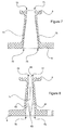
- Figure 7 shows an exemplary cross-section of the transition in the H plane (i.e. the long dimension of the transition passage lies in the plane of the paper).
- This shows the form of the side walls, which may be shaped at points 70, 71 to join smoothly with a rectangular dominant mode waveguide at the rectangular end.
- the side walls are also shaped at points 72, 73 to join smoothly with an elliptical overmoded waveguide at the elliptical end (although this shaping is optional, as discussed above).
- the side walls are smooth along their lengths, without any discontinuities which would cause undesirable mode conversion.
- Figure 7 also shows a pair of slots 74, 75 formed in the side walls. These slots may be centered on the H plane and are configured to receive a mode filter, such as that described below.
- Figure 8 shows an exemplary cross-section of the waveguide transition in the E plane (i.e. the short dimension of the transition passage lies in the plane of the paper).
- This shows the form of the top and bottom walls, which may be shaped at points 76, 77 to join smoothly with a rectangular dominant mode waveguide at the rectangular end.
- the top and bottom walls may also be shaped at points 78, 79 to join smoothly with an elliptical overmoded waveguide at the elliptical end.
- This Figure also shows the shape of the side walls and the slot 74 projected onto the cross-section.
- the height of the side walls (indicated by lines 80, 81) may taper continuously along the length of the transition, from the height of the rectangle at point 82 at the rectangular end, to zero at point 83 at the elliptical end.
- the mode filter card 84 may be generally trapezoidal in shape, matching the shape of the slots 74, 75 (as can be seen in Figure 7 ) such that the card 84 is easily fitted into the slots 74, 75 but is snugly retained therein.
- any suitable shape of the slots and of the mode filter card may be used, with these two shapes generally cooperating to allow positioning and retention of the mode filter card.
- Such a mode filter may consist of a resistive card, such as a mylar substrate 85 with a resistive coating 86 as shown in Figure 11 .
- the coating 86 may be a metallic coating and may be sputtered or vacuum deposited on to the substrate 85.
- the resistive material 86 may be made to Florida RF Labs specifications and may be deposited in a single process rather than in layers.
- the resistive coating may have a resistivity of between 100 ohms/square and 1000 ohms/square and may be formed of chrome and nickel, or an absorbtive coating such as carbon. Any resistive material may be suitable.
- the resistivity of the coating may be chosen such that there is an adequate absorption of the higher-order modes without causing an unacceptable absorption of the dominant mode. The resistivity required may depend on the total length of the mode filter, and/or other system parameters.
- the abrupt edges of the mode filter may also generate modes.
- the superior design of the Applicant's transition gives it a performance without any mode filters which is close to the performance of some prior art connectors with filters for certain lengths of cable.
- the resistive material of the mode filter may also be patterned during deposition, etched or otherwise processed to provide any suitable pattern of resistive material.
- the mode filter card could be patterned such that the resistive material is positioned adjacent the transition's side walls, with a clear strip running down the middle of the mode filter card.
- the substrate material 85 could be any suitable dielectric such as mylar, fiberglass, mica, etc.
- the substrate material chosen should be able to withstand the temperatures generated in the waveguide transition and in the resistive material.
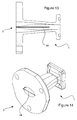
- Figure 12 is a cross-section of a waveguide transition showing the mode filter card in place.
- the filter may take up approximately 75% of the transition length, ensuring that there is adequate filtering in that part of the transition which is dimensioned such that higher modes may exist. This percentage of the transition length may be different depending on transition length, resistivity of the resistive coating and desired attenuating properties of the mode filter.
- Figure 13 is a second cross-section, showing the transition from the side. With the filter positioned in this way, unwanted higher modes induce a current in the resistive coating. This current experiences losses because of the resistance of the coating, effectively attenuating the higher modes. The desired signals in the fundamental mode pass by without inducing a current in the resistive coating and therefore with significantly lower attenuation.
- a mode filter is simply fitted to the slots 74 and 75 at the elliptical end and slid into position before attachment of an elliptical overmoded waveguide to the transition.
- Figure 14 shows a perspective view of the transition 1 from the elliptical end 3, with the mode filter card 84 in place.
- Figure 15 shows a plot of insertion loss as a function of frequency for a conventional waveguide transition with no mode filtration. This plot therefore illustrates the inherent mode conversion of this transition.
- the conventional transition is a transition for connecting an elliptical overmoded waveguide to a rectangular dominant mode waveguide, and has an internal shape consisting of an elliptical bore intersecting a rectangular pyramid.
- FIG. 16 shows a similar plot to that of Figure 15 , for the applicant's transition fabricated according to the embodiment described above. The scale is identical to that of Figure 15 , and it is clear that the amplitude of the spikes is significantly lower than the existing product (about 25%), indicating that mode conversion is significantly lower in the applicant's transition than in the conventional transition.
- This lower mode conversion allows the applicant's transition to be used with a much lower level of mode filtration. Since mode filtration necessarily also attenuates the desired fundamental mode signals, the applicant's transition can provide similar levels of unwanted higher mode signals to existing products and a dramatic reduction in fundamental mode attenuation. Alternatively, higher levels of mode filtering could be used, to achieve significantly lower levels of unwanted higher mode signals than in existing products and a similar level of fundamental mode attenuation.
- the applicant's transition also provides very low voltage standing wave ratio (VSWR) over a very wide band, a critical requirement for a waveguide transition.
- VSWR voltage standing wave ratio
- a waveguide system may include a rectangular dominant mode waveguide input, a first transition from the rectangular waveguide to an elliptical overmoded waveguide, a length of elliptical overmoded waveguide, and a second transition from the elliptical overmoded waveguide to a rectangular dominant mode waveguide output.
- these higher modes should be effectively filtered and should not convert back to the fundamental mode, since this causes signal distortion.
- a waveguide system was set up, with a length of elliptical waveguide and two transitions, forming a cavity supporting higher modes.
- the maximum peak-to-peak ripple in the insertion loss was measured over the operating frequency range ("the higher mode level").
- a first measurement of the higher mode level was taken with the elliptical waveguide in a substantially straight configuration, and a second measurement was taken with two 90° bends formed in the elliptical waveguide at the minimum bend radius of the waveguide.
- the higher mode level increased from 23dB to 1.0dB.
- the applicant's transition was essentially the same whether the waveguide was straight or bent, being 0.23dB in both configurations.
- the component may be a waveguide transition (including, but not limited to, a taper transition for transitioning between any combination of rectangular, elliptical, circular or square waveguides, such as rectangular-to-rectangular, rectangular-to-elliptical, rectangular-to-square, elliptical-to-circular, elliptical-to-elliptical etc; and any combination of dominant mode and overmoded waveguides).
- the component may also be a transition for transitioning between a coaxial transmission line and a waveguide of any cross-section.
- the component may also be a waveguide connector or joint, or any other suitable component.
- the waveguide component may be designed such that its shape allows it to be formed in a single piece. Since the method involves a casting process, this means that the internal shape of the component should be advantageously configured for removal of a mold core after casting.
- This internal shape may be an internal taper, allowing the mold core to be removed from one end of the component.
- the internal taper may be a continuous, smooth taper from one end of the component to the other. Such removal of the mold core also allows reuse of this part, which is of course desirable from a cost perspective.
- Formation in a single piece provides a component with a better quality inner surface, without the joins necessary in component made in two or more pieces. Such joins may cause undesirable reflections and/or mode conversion. Also, further assembly and/or machining steps are not required where the component is formed in a single piece.
- the waveguide component is capable of fabrication by thixoforming. This is a casting process, which allows fabrication with extremely precise tolerances.
- a metallic material is introduced into a thixotropic state, in which both liquid and solid phases are present. This may be performed by heating a stock material. Shear forces may be applied, preventing the formation of structures in the thixotropic material. The material is then injection molded in this thixotropic state.
- a suitable thixoforming process is that used by Thixomat, Inc of Ann Arbor, Michigan. Other processes may also be suitable.
- the metallic material may be a metal alloy, and in particular may be a magnesium alloy, such as alloy AZ91 D.
- This alloy is composed principally of magnesium with other elements in the following proportions:
- Magnesium alloy is mechanically strong and is generally somewhat lighter and less costly than the copper-based materials previously used in waveguide components made by electroforming.
- This fabrication method allows accurate fabrication of a waveguide component. Unlike conventional casting processes, no binder or sintering is generally required and the process may allow very tight tolerance control (approximately ⁇ 0.001").
- the component when released from its mold and with the mold core removed may be substantially in its finished state, requiring little additional machining.
- Features such as flanges, slots, grooves, apertures for coupling to waveguides or waveguide components, etc may be formed during the molding process. This is in contrast to other fabrication methods, which either require additional fabrication steps or do not produce the required precision.
- formation of the component in a single piece, as described herein means that the internal shape of the component is formed as a single piece. Of course, this single piece may subsequently be joined to any number of external features, such as flanges and the like, and remain within the scope of the invention.
- the fabrication process described above may be advantageous for fabrication of waveguide components and transitions in general.
- the fabrication method may be especially advantageous for fabrication of transitions for connecting an overmoded waveguide to another waveguide, because of the tight tolerances required for avoidance of mode conversion.
- the waveguide transition described above requires extremely precise fabrication, to give a smooth and accurate internal surface, and this fabrication method meets these criteria. Furthermore, this transition is designed with a continuous internal taper and with the mode filter slot exiting at the wider end. This enables removal of a mold core after formation.
- While the waveguide transition described above transitions from a dominant mode rectangular waveguide to an elliptical overmoded waveguide, similar transitions are also within the scope of the invention, including: transitions from rectangular overmoded waveguides to elliptical overmoded waveguides; and transitions from rectangular overmoded waveguides to elliptical dominant moded waveguides.
- the rectangular end will be of dimensions generally larger than the elliptical end.
- the same principles and mathematical functions set out above can be used in such a transition.
- the term "elliptical” as commonly applied to waveguides is merely an approximation, and does not necessarily imply a shape meeting the mathematical criteria of a true ellipse.
- the term “elliptical” or “ellipse” is intended to embrace not just cross-sectional configurations which are mathematically true ellipses, but also cross-sectional configurations which are oval, circular, quasi-elliptical, or super-elliptical (as described in US 4,642,585 , for example).
- the invention is applicable to any of these cross-sectional configurations, including the more or less oval-shaped configurations commonly called “elliptical” in the waveguide art.
- a circular waveguide is simply a special case of an elliptical waveguide, and is intended to be within the scope of the invention.
- a square waveguide is a special case of a rectangular waveguide and is also intended to be within the scope of the invention.
- the waveguide transition may be described herein as transitioning from a rectangular waveguide to an elliptical waveguide, or from a dominant mode waveguide to an overmoded waveguide, the transition is adapted to transmit signals in both directions.
- the transition may be described as having an input end and an output end, this is simply for convenience of description and should not be taken as limiting.
Landscapes
- Engineering & Computer Science (AREA)
- Mechanical Engineering (AREA)
- Control Of Motors That Do Not Use Commutators (AREA)
Applications Claiming Priority (1)
| Application Number | Priority Date | Filing Date | Title |
|---|---|---|---|
| US11/637,478 US7893789B2 (en) | 2006-12-12 | 2006-12-12 | Waveguide transitions and method of forming components |
Publications (2)
| Publication Number | Publication Date |
|---|---|
| EP1933412A2 true EP1933412A2 (de) | 2008-06-18 |
| EP1933412A3 EP1933412A3 (de) | 2008-12-17 |
Family
ID=39247285
Family Applications (1)
| Application Number | Title | Priority Date | Filing Date |
|---|---|---|---|
| EP07122734A Ceased EP1933412A3 (de) | 2006-12-12 | 2007-12-10 | Wellenleiterübergänge und Verfahren zur Herstellung von Komponenten dafür |
Country Status (5)
| Country | Link |
|---|---|
| US (1) | US7893789B2 (de) |
| EP (1) | EP1933412A3 (de) |
| BR (1) | BRPI0704442A (de) |
| CA (1) | CA2608917A1 (de) |
| MX (1) | MX2007015795A (de) |
Cited By (4)
| Publication number | Priority date | Publication date | Assignee | Title |
|---|---|---|---|---|
| EP2058896A1 (de) * | 2007-11-09 | 2009-05-13 | Thales | Verfahren zur Herstellung einer als dicken Platte elektrogeformten Monoblock-Mikrowelle |
| FR2940519A1 (fr) * | 2008-12-23 | 2010-06-25 | Thales Sa | Transition adaptee de sortie rf pour tube electronique hyperfrequences de puissance |
| CN102394332A (zh) * | 2011-07-15 | 2012-03-28 | 中国工程物理研究院电子工程研究所 | 一种幂函数赋形的宽带te01模口径转换器 |
| WO2015076885A1 (en) * | 2013-11-19 | 2015-05-28 | Commscope Technologies Llc | Modular feed assembly |
Families Citing this family (171)
| Publication number | Priority date | Publication date | Assignee | Title |
|---|---|---|---|---|
| US8384605B2 (en) * | 2009-02-25 | 2013-02-26 | Sikorsky Aircraft Corporation | Wireless communication between a rotating frame of reference and a non-rotating frame of reference |
| US8816791B2 (en) | 2010-09-28 | 2014-08-26 | Aviat U.S., Inc. | Systems and methods of a rectangular-to-circular waveguide transition |
| US9166278B2 (en) | 2010-09-29 | 2015-10-20 | Nec Corporation | Communication apparatus |
| CN102569966A (zh) * | 2011-12-30 | 2012-07-11 | 零八一电子集团四川华昌电子有限公司 | 长厘米波段超短型矩圆过渡波导 |
| US10009065B2 (en) | 2012-12-05 | 2018-06-26 | At&T Intellectual Property I, L.P. | Backhaul link for distributed antenna system |
| US9113347B2 (en) | 2012-12-05 | 2015-08-18 | At&T Intellectual Property I, Lp | Backhaul link for distributed antenna system |
| US9525524B2 (en) | 2013-05-31 | 2016-12-20 | At&T Intellectual Property I, L.P. | Remote distributed antenna system |
| US9999038B2 (en) | 2013-05-31 | 2018-06-12 | At&T Intellectual Property I, L.P. | Remote distributed antenna system |
| US9281550B2 (en) | 2013-07-16 | 2016-03-08 | L&J Engineering, Inc. | Wave mode converter |
| US8897697B1 (en) | 2013-11-06 | 2014-11-25 | At&T Intellectual Property I, Lp | Millimeter-wave surface-wave communications |
| US9209902B2 (en) | 2013-12-10 | 2015-12-08 | At&T Intellectual Property I, L.P. | Quasi-optical coupler |
| CN103639374B (zh) * | 2013-12-18 | 2016-05-11 | 北京科技大学 | 一种制备半固态金属的振动倒锥形通道方法及装置 |
| US9692101B2 (en) | 2014-08-26 | 2017-06-27 | At&T Intellectual Property I, L.P. | Guided wave couplers for coupling electromagnetic waves between a waveguide surface and a surface of a wire |
| US9768833B2 (en) | 2014-09-15 | 2017-09-19 | At&T Intellectual Property I, L.P. | Method and apparatus for sensing a condition in a transmission medium of electromagnetic waves |
| US10063280B2 (en) | 2014-09-17 | 2018-08-28 | At&T Intellectual Property I, L.P. | Monitoring and mitigating conditions in a communication network |
| US9628854B2 (en) | 2014-09-29 | 2017-04-18 | At&T Intellectual Property I, L.P. | Method and apparatus for distributing content in a communication network |
| US9615269B2 (en) | 2014-10-02 | 2017-04-04 | At&T Intellectual Property I, L.P. | Method and apparatus that provides fault tolerance in a communication network |
| US9685992B2 (en) | 2014-10-03 | 2017-06-20 | At&T Intellectual Property I, L.P. | Circuit panel network and methods thereof |
| US9503189B2 (en) | 2014-10-10 | 2016-11-22 | At&T Intellectual Property I, L.P. | Method and apparatus for arranging communication sessions in a communication system |
| US9973299B2 (en) | 2014-10-14 | 2018-05-15 | At&T Intellectual Property I, L.P. | Method and apparatus for adjusting a mode of communication in a communication network |
| US9762289B2 (en) | 2014-10-14 | 2017-09-12 | At&T Intellectual Property I, L.P. | Method and apparatus for transmitting or receiving signals in a transportation system |
| US9520945B2 (en) | 2014-10-21 | 2016-12-13 | At&T Intellectual Property I, L.P. | Apparatus for providing communication services and methods thereof |
| US9627768B2 (en) | 2014-10-21 | 2017-04-18 | At&T Intellectual Property I, L.P. | Guided-wave transmission device with non-fundamental mode propagation and methods for use therewith |
| US9653770B2 (en) | 2014-10-21 | 2017-05-16 | At&T Intellectual Property I, L.P. | Guided wave coupler, coupling module and methods for use therewith |
| US9577306B2 (en) | 2014-10-21 | 2017-02-21 | At&T Intellectual Property I, L.P. | Guided-wave transmission device and methods for use therewith |
| US9769020B2 (en) | 2014-10-21 | 2017-09-19 | At&T Intellectual Property I, L.P. | Method and apparatus for responding to events affecting communications in a communication network |
| US9564947B2 (en) | 2014-10-21 | 2017-02-07 | At&T Intellectual Property I, L.P. | Guided-wave transmission device with diversity and methods for use therewith |
| US9780834B2 (en) | 2014-10-21 | 2017-10-03 | At&T Intellectual Property I, L.P. | Method and apparatus for transmitting electromagnetic waves |
| US9312919B1 (en) | 2014-10-21 | 2016-04-12 | At&T Intellectual Property I, Lp | Transmission device with impairment compensation and methods for use therewith |
| US9800327B2 (en) | 2014-11-20 | 2017-10-24 | At&T Intellectual Property I, L.P. | Apparatus for controlling operations of a communication device and methods thereof |
| US10340573B2 (en) | 2016-10-26 | 2019-07-02 | At&T Intellectual Property I, L.P. | Launcher with cylindrical coupling device and methods for use therewith |
| US10009067B2 (en) | 2014-12-04 | 2018-06-26 | At&T Intellectual Property I, L.P. | Method and apparatus for configuring a communication interface |
| US9461706B1 (en) | 2015-07-31 | 2016-10-04 | At&T Intellectual Property I, Lp | Method and apparatus for exchanging communication signals |
| US9742462B2 (en) | 2014-12-04 | 2017-08-22 | At&T Intellectual Property I, L.P. | Transmission medium and communication interfaces and methods for use therewith |
| US10243784B2 (en) | 2014-11-20 | 2019-03-26 | At&T Intellectual Property I, L.P. | System for generating topology information and methods thereof |
| US9997819B2 (en) | 2015-06-09 | 2018-06-12 | At&T Intellectual Property I, L.P. | Transmission medium and method for facilitating propagation of electromagnetic waves via a core |
| US9680670B2 (en) | 2014-11-20 | 2017-06-13 | At&T Intellectual Property I, L.P. | Transmission device with channel equalization and control and methods for use therewith |
| US9654173B2 (en) | 2014-11-20 | 2017-05-16 | At&T Intellectual Property I, L.P. | Apparatus for powering a communication device and methods thereof |
| US9544006B2 (en) | 2014-11-20 | 2017-01-10 | At&T Intellectual Property I, L.P. | Transmission device with mode division multiplexing and methods for use therewith |
| US9954287B2 (en) | 2014-11-20 | 2018-04-24 | At&T Intellectual Property I, L.P. | Apparatus for converting wireless signals and electromagnetic waves and methods thereof |
| US10144036B2 (en) | 2015-01-30 | 2018-12-04 | At&T Intellectual Property I, L.P. | Method and apparatus for mitigating interference affecting a propagation of electromagnetic waves guided by a transmission medium |
| US9876570B2 (en) | 2015-02-20 | 2018-01-23 | At&T Intellectual Property I, Lp | Guided-wave transmission device with non-fundamental mode propagation and methods for use therewith |
| US9749013B2 (en) | 2015-03-17 | 2017-08-29 | At&T Intellectual Property I, L.P. | Method and apparatus for reducing attenuation of electromagnetic waves guided by a transmission medium |
| US10224981B2 (en) | 2015-04-24 | 2019-03-05 | At&T Intellectual Property I, Lp | Passive electrical coupling device and methods for use therewith |
| US9705561B2 (en) | 2015-04-24 | 2017-07-11 | At&T Intellectual Property I, L.P. | Directional coupling device and methods for use therewith |
| US9948354B2 (en) | 2015-04-28 | 2018-04-17 | At&T Intellectual Property I, L.P. | Magnetic coupling device with reflective plate and methods for use therewith |
| US9793954B2 (en) | 2015-04-28 | 2017-10-17 | At&T Intellectual Property I, L.P. | Magnetic coupling device and methods for use therewith |
| US9748626B2 (en) | 2015-05-14 | 2017-08-29 | At&T Intellectual Property I, L.P. | Plurality of cables having different cross-sectional shapes which are bundled together to form a transmission medium |
| US9490869B1 (en) | 2015-05-14 | 2016-11-08 | At&T Intellectual Property I, L.P. | Transmission medium having multiple cores and methods for use therewith |
| US9871282B2 (en) | 2015-05-14 | 2018-01-16 | At&T Intellectual Property I, L.P. | At least one transmission medium having a dielectric surface that is covered at least in part by a second dielectric |
| US10650940B2 (en) | 2015-05-15 | 2020-05-12 | At&T Intellectual Property I, L.P. | Transmission medium having a conductive material and methods for use therewith |
| US10679767B2 (en) | 2015-05-15 | 2020-06-09 | At&T Intellectual Property I, L.P. | Transmission medium having a conductive material and methods for use therewith |
| US9917341B2 (en) | 2015-05-27 | 2018-03-13 | At&T Intellectual Property I, L.P. | Apparatus and method for launching electromagnetic waves and for modifying radial dimensions of the propagating electromagnetic waves |
| US9912381B2 (en) | 2015-06-03 | 2018-03-06 | At&T Intellectual Property I, Lp | Network termination and methods for use therewith |
| US10154493B2 (en) | 2015-06-03 | 2018-12-11 | At&T Intellectual Property I, L.P. | Network termination and methods for use therewith |
| US10348391B2 (en) | 2015-06-03 | 2019-07-09 | At&T Intellectual Property I, L.P. | Client node device with frequency conversion and methods for use therewith |
| US10103801B2 (en) | 2015-06-03 | 2018-10-16 | At&T Intellectual Property I, L.P. | Host node device and methods for use therewith |
| US9866309B2 (en) | 2015-06-03 | 2018-01-09 | At&T Intellectual Property I, Lp | Host node device and methods for use therewith |
| US10812174B2 (en) | 2015-06-03 | 2020-10-20 | At&T Intellectual Property I, L.P. | Client node device and methods for use therewith |
| US9913139B2 (en) | 2015-06-09 | 2018-03-06 | At&T Intellectual Property I, L.P. | Signal fingerprinting for authentication of communicating devices |
| US10142086B2 (en) | 2015-06-11 | 2018-11-27 | At&T Intellectual Property I, L.P. | Repeater and methods for use therewith |
| US9608692B2 (en) | 2015-06-11 | 2017-03-28 | At&T Intellectual Property I, L.P. | Repeater and methods for use therewith |
| US9820146B2 (en) | 2015-06-12 | 2017-11-14 | At&T Intellectual Property I, L.P. | Method and apparatus for authentication and identity management of communicating devices |
| US9667317B2 (en) | 2015-06-15 | 2017-05-30 | At&T Intellectual Property I, L.P. | Method and apparatus for providing security using network traffic adjustments |
| US9509415B1 (en) * | 2015-06-25 | 2016-11-29 | At&T Intellectual Property I, L.P. | Methods and apparatus for inducing a fundamental wave mode on a transmission medium |
| US9640850B2 (en) | 2015-06-25 | 2017-05-02 | At&T Intellectual Property I, L.P. | Methods and apparatus for inducing a non-fundamental wave mode on a transmission medium |
| US9865911B2 (en) | 2015-06-25 | 2018-01-09 | At&T Intellectual Property I, L.P. | Waveguide system for slot radiating first electromagnetic waves that are combined into a non-fundamental wave mode second electromagnetic wave on a transmission medium |
| US9628116B2 (en) | 2015-07-14 | 2017-04-18 | At&T Intellectual Property I, L.P. | Apparatus and methods for transmitting wireless signals |
| US10033108B2 (en) | 2015-07-14 | 2018-07-24 | At&T Intellectual Property I, L.P. | Apparatus and methods for generating an electromagnetic wave having a wave mode that mitigates interference |
| US10148016B2 (en) | 2015-07-14 | 2018-12-04 | At&T Intellectual Property I, L.P. | Apparatus and methods for communicating utilizing an antenna array |
| US10170840B2 (en) | 2015-07-14 | 2019-01-01 | At&T Intellectual Property I, L.P. | Apparatus and methods for sending or receiving electromagnetic signals |
| US9853342B2 (en) | 2015-07-14 | 2017-12-26 | At&T Intellectual Property I, L.P. | Dielectric transmission medium connector and methods for use therewith |
| US10033107B2 (en) | 2015-07-14 | 2018-07-24 | At&T Intellectual Property I, L.P. | Method and apparatus for coupling an antenna to a device |
| US9882257B2 (en) | 2015-07-14 | 2018-01-30 | At&T Intellectual Property I, L.P. | Method and apparatus for launching a wave mode that mitigates interference |
| US9836957B2 (en) | 2015-07-14 | 2017-12-05 | At&T Intellectual Property I, L.P. | Method and apparatus for communicating with premises equipment |
| US10044409B2 (en) | 2015-07-14 | 2018-08-07 | At&T Intellectual Property I, L.P. | Transmission medium and methods for use therewith |
| US10205655B2 (en) | 2015-07-14 | 2019-02-12 | At&T Intellectual Property I, L.P. | Apparatus and methods for communicating utilizing an antenna array and multiple communication paths |
| US9722318B2 (en) | 2015-07-14 | 2017-08-01 | At&T Intellectual Property I, L.P. | Method and apparatus for coupling an antenna to a device |
| US9847566B2 (en) | 2015-07-14 | 2017-12-19 | At&T Intellectual Property I, L.P. | Method and apparatus for adjusting a field of a signal to mitigate interference |
| US10320586B2 (en) | 2015-07-14 | 2019-06-11 | At&T Intellectual Property I, L.P. | Apparatus and methods for generating non-interfering electromagnetic waves on an insulated transmission medium |
| US10341142B2 (en) | 2015-07-14 | 2019-07-02 | At&T Intellectual Property I, L.P. | Apparatus and methods for generating non-interfering electromagnetic waves on an uninsulated conductor |
| US10090606B2 (en) | 2015-07-15 | 2018-10-02 | At&T Intellectual Property I, L.P. | Antenna system with dielectric array and methods for use therewith |
| US9608740B2 (en) | 2015-07-15 | 2017-03-28 | At&T Intellectual Property I, L.P. | Method and apparatus for launching a wave mode that mitigates interference |
| US9793951B2 (en) | 2015-07-15 | 2017-10-17 | At&T Intellectual Property I, L.P. | Method and apparatus for launching a wave mode that mitigates interference |
| US9871283B2 (en) | 2015-07-23 | 2018-01-16 | At&T Intellectual Property I, Lp | Transmission medium having a dielectric core comprised of plural members connected by a ball and socket configuration |
| US9749053B2 (en) | 2015-07-23 | 2017-08-29 | At&T Intellectual Property I, L.P. | Node device, repeater and methods for use therewith |
| US9912027B2 (en) | 2015-07-23 | 2018-03-06 | At&T Intellectual Property I, L.P. | Method and apparatus for exchanging communication signals |
| US10784670B2 (en) | 2015-07-23 | 2020-09-22 | At&T Intellectual Property I, L.P. | Antenna support for aligning an antenna |
| US9948333B2 (en) | 2015-07-23 | 2018-04-17 | At&T Intellectual Property I, L.P. | Method and apparatus for wireless communications to mitigate interference |
| US9735833B2 (en) | 2015-07-31 | 2017-08-15 | At&T Intellectual Property I, L.P. | Method and apparatus for communications management in a neighborhood network |
| US10020587B2 (en) | 2015-07-31 | 2018-07-10 | At&T Intellectual Property I, L.P. | Radial antenna and methods for use therewith |
| US9967173B2 (en) | 2015-07-31 | 2018-05-08 | At&T Intellectual Property I, L.P. | Method and apparatus for authentication and identity management of communicating devices |
| US9904535B2 (en) | 2015-09-14 | 2018-02-27 | At&T Intellectual Property I, L.P. | Method and apparatus for distributing software |
| US10009901B2 (en) | 2015-09-16 | 2018-06-26 | At&T Intellectual Property I, L.P. | Method, apparatus, and computer-readable storage medium for managing utilization of wireless resources between base stations |
| US9705571B2 (en) | 2015-09-16 | 2017-07-11 | At&T Intellectual Property I, L.P. | Method and apparatus for use with a radio distributed antenna system |
| US10079661B2 (en) | 2015-09-16 | 2018-09-18 | At&T Intellectual Property I, L.P. | Method and apparatus for use with a radio distributed antenna system having a clock reference |
| US10136434B2 (en) | 2015-09-16 | 2018-11-20 | At&T Intellectual Property I, L.P. | Method and apparatus for use with a radio distributed antenna system having an ultra-wideband control channel |
| US10009063B2 (en) | 2015-09-16 | 2018-06-26 | At&T Intellectual Property I, L.P. | Method and apparatus for use with a radio distributed antenna system having an out-of-band reference signal |
| US10051629B2 (en) | 2015-09-16 | 2018-08-14 | At&T Intellectual Property I, L.P. | Method and apparatus for use with a radio distributed antenna system having an in-band reference signal |
| US9769128B2 (en) | 2015-09-28 | 2017-09-19 | At&T Intellectual Property I, L.P. | Method and apparatus for encryption of communications over a network |
| US9729197B2 (en) | 2015-10-01 | 2017-08-08 | At&T Intellectual Property I, L.P. | Method and apparatus for communicating network management traffic over a network |
| US10074890B2 (en) | 2015-10-02 | 2018-09-11 | At&T Intellectual Property I, L.P. | Communication device and antenna with integrated light assembly |
| US9876264B2 (en) | 2015-10-02 | 2018-01-23 | At&T Intellectual Property I, Lp | Communication system, guided wave switch and methods for use therewith |
| US9882277B2 (en) | 2015-10-02 | 2018-01-30 | At&T Intellectual Property I, Lp | Communication device and antenna assembly with actuated gimbal mount |
| US10665942B2 (en) | 2015-10-16 | 2020-05-26 | At&T Intellectual Property I, L.P. | Method and apparatus for adjusting wireless communications |
| US10355367B2 (en) | 2015-10-16 | 2019-07-16 | At&T Intellectual Property I, L.P. | Antenna structure for exchanging wireless signals |
| US10051483B2 (en) | 2015-10-16 | 2018-08-14 | At&T Intellectual Property I, L.P. | Method and apparatus for directing wireless signals |
| US9912419B1 (en) | 2016-08-24 | 2018-03-06 | At&T Intellectual Property I, L.P. | Method and apparatus for managing a fault in a distributed antenna system |
| US9860075B1 (en) | 2016-08-26 | 2018-01-02 | At&T Intellectual Property I, L.P. | Method and communication node for broadband distribution |
| US10291311B2 (en) | 2016-09-09 | 2019-05-14 | At&T Intellectual Property I, L.P. | Method and apparatus for mitigating a fault in a distributed antenna system |
| US11032819B2 (en) | 2016-09-15 | 2021-06-08 | At&T Intellectual Property I, L.P. | Method and apparatus for use with a radio distributed antenna system having a control channel reference signal |
| US10135147B2 (en) | 2016-10-18 | 2018-11-20 | At&T Intellectual Property I, L.P. | Apparatus and methods for launching guided waves via an antenna |
| US10135146B2 (en) | 2016-10-18 | 2018-11-20 | At&T Intellectual Property I, L.P. | Apparatus and methods for launching guided waves via circuits |
| US10340600B2 (en) | 2016-10-18 | 2019-07-02 | At&T Intellectual Property I, L.P. | Apparatus and methods for launching guided waves via plural waveguide systems |
| US10811767B2 (en) | 2016-10-21 | 2020-10-20 | At&T Intellectual Property I, L.P. | System and dielectric antenna with convex dielectric radome |
| US9876605B1 (en) | 2016-10-21 | 2018-01-23 | At&T Intellectual Property I, L.P. | Launcher and coupling system to support desired guided wave mode |
| US10374316B2 (en) | 2016-10-21 | 2019-08-06 | At&T Intellectual Property I, L.P. | System and dielectric antenna with non-uniform dielectric |
| US9991580B2 (en) | 2016-10-21 | 2018-06-05 | At&T Intellectual Property I, L.P. | Launcher and coupling system for guided wave mode cancellation |
| US10312567B2 (en) | 2016-10-26 | 2019-06-04 | At&T Intellectual Property I, L.P. | Launcher with planar strip antenna and methods for use therewith |
| US10225025B2 (en) | 2016-11-03 | 2019-03-05 | At&T Intellectual Property I, L.P. | Method and apparatus for detecting a fault in a communication system |
| US10498044B2 (en) | 2016-11-03 | 2019-12-03 | At&T Intellectual Property I, L.P. | Apparatus for configuring a surface of an antenna |
| US10291334B2 (en) | 2016-11-03 | 2019-05-14 | At&T Intellectual Property I, L.P. | System for detecting a fault in a communication system |
| US10224634B2 (en) | 2016-11-03 | 2019-03-05 | At&T Intellectual Property I, L.P. | Methods and apparatus for adjusting an operational characteristic of an antenna |
| US10090594B2 (en) | 2016-11-23 | 2018-10-02 | At&T Intellectual Property I, L.P. | Antenna system having structural configurations for assembly |
| US10535928B2 (en) | 2016-11-23 | 2020-01-14 | At&T Intellectual Property I, L.P. | Antenna system and methods for use therewith |
| US10178445B2 (en) | 2016-11-23 | 2019-01-08 | At&T Intellectual Property I, L.P. | Methods, devices, and systems for load balancing between a plurality of waveguides |
| US10340603B2 (en) | 2016-11-23 | 2019-07-02 | At&T Intellectual Property I, L.P. | Antenna system having shielded structural configurations for assembly |
| US10340601B2 (en) | 2016-11-23 | 2019-07-02 | At&T Intellectual Property I, L.P. | Multi-antenna system and methods for use therewith |
| US10361489B2 (en) | 2016-12-01 | 2019-07-23 | At&T Intellectual Property I, L.P. | Dielectric dish antenna system and methods for use therewith |
| US10305190B2 (en) | 2016-12-01 | 2019-05-28 | At&T Intellectual Property I, L.P. | Reflecting dielectric antenna system and methods for use therewith |
| US10382976B2 (en) | 2016-12-06 | 2019-08-13 | At&T Intellectual Property I, L.P. | Method and apparatus for managing wireless communications based on communication paths and network device positions |
| US10727599B2 (en) | 2016-12-06 | 2020-07-28 | At&T Intellectual Property I, L.P. | Launcher with slot antenna and methods for use therewith |
| US10135145B2 (en) | 2016-12-06 | 2018-11-20 | At&T Intellectual Property I, L.P. | Apparatus and methods for generating an electromagnetic wave along a transmission medium |
| US10694379B2 (en) | 2016-12-06 | 2020-06-23 | At&T Intellectual Property I, L.P. | Waveguide system with device-based authentication and methods for use therewith |
| US10819035B2 (en) | 2016-12-06 | 2020-10-27 | At&T Intellectual Property I, L.P. | Launcher with helical antenna and methods for use therewith |
| US10020844B2 (en) | 2016-12-06 | 2018-07-10 | T&T Intellectual Property I, L.P. | Method and apparatus for broadcast communication via guided waves |
| US10637149B2 (en) | 2016-12-06 | 2020-04-28 | At&T Intellectual Property I, L.P. | Injection molded dielectric antenna and methods for use therewith |
| US10326494B2 (en) | 2016-12-06 | 2019-06-18 | At&T Intellectual Property I, L.P. | Apparatus for measurement de-embedding and methods for use therewith |
| US10755542B2 (en) | 2016-12-06 | 2020-08-25 | At&T Intellectual Property I, L.P. | Method and apparatus for surveillance via guided wave communication |
| US10439675B2 (en) | 2016-12-06 | 2019-10-08 | At&T Intellectual Property I, L.P. | Method and apparatus for repeating guided wave communication signals |
| US9927517B1 (en) | 2016-12-06 | 2018-03-27 | At&T Intellectual Property I, L.P. | Apparatus and methods for sensing rainfall |
| US10446936B2 (en) | 2016-12-07 | 2019-10-15 | At&T Intellectual Property I, L.P. | Multi-feed dielectric antenna system and methods for use therewith |
| US10389029B2 (en) | 2016-12-07 | 2019-08-20 | At&T Intellectual Property I, L.P. | Multi-feed dielectric antenna system with core selection and methods for use therewith |
| US10027397B2 (en) | 2016-12-07 | 2018-07-17 | At&T Intellectual Property I, L.P. | Distributed antenna system and methods for use therewith |
| US10139820B2 (en) | 2016-12-07 | 2018-11-27 | At&T Intellectual Property I, L.P. | Method and apparatus for deploying equipment of a communication system |
| US10243270B2 (en) | 2016-12-07 | 2019-03-26 | At&T Intellectual Property I, L.P. | Beam adaptive multi-feed dielectric antenna system and methods for use therewith |
| US9893795B1 (en) | 2016-12-07 | 2018-02-13 | At&T Intellectual Property I, Lp | Method and repeater for broadband distribution |
| US10168695B2 (en) | 2016-12-07 | 2019-01-01 | At&T Intellectual Property I, L.P. | Method and apparatus for controlling an unmanned aircraft |
| US10547348B2 (en) | 2016-12-07 | 2020-01-28 | At&T Intellectual Property I, L.P. | Method and apparatus for switching transmission mediums in a communication system |
| US10359749B2 (en) | 2016-12-07 | 2019-07-23 | At&T Intellectual Property I, L.P. | Method and apparatus for utilities management via guided wave communication |
| US10389037B2 (en) | 2016-12-08 | 2019-08-20 | At&T Intellectual Property I, L.P. | Apparatus and methods for selecting sections of an antenna array and use therewith |
| US10530505B2 (en) | 2016-12-08 | 2020-01-07 | At&T Intellectual Property I, L.P. | Apparatus and methods for launching electromagnetic waves along a transmission medium |
| US10103422B2 (en) | 2016-12-08 | 2018-10-16 | At&T Intellectual Property I, L.P. | Method and apparatus for mounting network devices |
| US10777873B2 (en) | 2016-12-08 | 2020-09-15 | At&T Intellectual Property I, L.P. | Method and apparatus for mounting network devices |
| US10411356B2 (en) | 2016-12-08 | 2019-09-10 | At&T Intellectual Property I, L.P. | Apparatus and methods for selectively targeting communication devices with an antenna array |
| US10601494B2 (en) | 2016-12-08 | 2020-03-24 | At&T Intellectual Property I, L.P. | Dual-band communication device and method for use therewith |
| US10916969B2 (en) | 2016-12-08 | 2021-02-09 | At&T Intellectual Property I, L.P. | Method and apparatus for providing power using an inductive coupling |
| US10938108B2 (en) | 2016-12-08 | 2021-03-02 | At&T Intellectual Property I, L.P. | Frequency selective multi-feed dielectric antenna system and methods for use therewith |
| US10069535B2 (en) | 2016-12-08 | 2018-09-04 | At&T Intellectual Property I, L.P. | Apparatus and methods for launching electromagnetic waves having a certain electric field structure |
| US9911020B1 (en) | 2016-12-08 | 2018-03-06 | At&T Intellectual Property I, L.P. | Method and apparatus for tracking via a radio frequency identification device |
| US10326689B2 (en) | 2016-12-08 | 2019-06-18 | At&T Intellectual Property I, L.P. | Method and system for providing alternative communication paths |
| US9998870B1 (en) | 2016-12-08 | 2018-06-12 | At&T Intellectual Property I, L.P. | Method and apparatus for proximity sensing |
| US10340983B2 (en) | 2016-12-09 | 2019-07-02 | At&T Intellectual Property I, L.P. | Method and apparatus for surveying remote sites via guided wave communications |
| US9838896B1 (en) | 2016-12-09 | 2017-12-05 | At&T Intellectual Property I, L.P. | Method and apparatus for assessing network coverage |
| US10264586B2 (en) | 2016-12-09 | 2019-04-16 | At&T Mobility Ii Llc | Cloud-based packet controller and methods for use therewith |
| US9973940B1 (en) | 2017-02-27 | 2018-05-15 | At&T Intellectual Property I, L.P. | Apparatus and methods for dynamic impedance matching of a guided wave launcher |
| US10298293B2 (en) | 2017-03-13 | 2019-05-21 | At&T Intellectual Property I, L.P. | Apparatus of communication utilizing wireless network devices |
| USD908641S1 (en) | 2017-11-30 | 2021-01-26 | Roos Instruments, Inc. | Blind mate waveguide flange |
| CN108682930B (zh) * | 2018-04-24 | 2024-03-26 | 中天射频电缆有限公司 | 一种端接波导过渡器 |
| US12537274B2 (en) * | 2024-04-04 | 2026-01-27 | The Boeing Company | Track transition systems for waveguide assemblies and related methods |
| CN120601112B (zh) * | 2025-08-08 | 2025-09-30 | 中国科学院合肥物质科学研究院 | 一种可自动进行模式优化的过模皱纹波导 |
Citations (1)
| Publication number | Priority date | Publication date | Assignee | Title |
|---|---|---|---|---|
| US4642585A (en) | 1985-01-30 | 1987-02-10 | Andrew Corporation | Superelliptical waveguide connection |
Family Cites Families (24)
| Publication number | Priority date | Publication date | Assignee | Title |
|---|---|---|---|---|
| GB1127910A (en) * | 1965-02-25 | 1968-09-18 | Telefunken Patent | Junction member for the connection of waveguides having different cross-sectional shapes |
| US3686595A (en) * | 1969-09-23 | 1972-08-22 | Georg Spinner | Waveguide transition member |
| US3818383A (en) * | 1973-02-27 | 1974-06-18 | Andrew Corp | Elliptical-to-rectangular waveguide transition |
| US3928825A (en) * | 1973-05-04 | 1975-12-23 | Licentia Gmbh | Waveguide transition piece with low reflection |
| GB1501405A (en) * | 1974-06-01 | 1978-02-15 | Licentia Gmbh | Arrangement with a hollow waveguide section |
| DE2737125C2 (de) | 1977-08-17 | 1985-10-03 | Spinner GmbH Elektrotechnische Fabrik, 8000 München | Übertragungssystem |
| DE2939562C2 (de) * | 1979-09-29 | 1982-09-09 | Licentia Patent-Verwaltungs-Gmbh, 6000 Frankfurt | Hornstrahler als Erreger für eine Reflektorantenne mit einem Hybridmoden-Anregungsteil |
| US4491810A (en) * | 1983-01-28 | 1985-01-01 | Andrew Corporation | Multi-port, multi-frequency microwave combiner with overmoded square waveguide section |
| FR2542928B1 (fr) * | 1983-03-18 | 1985-10-04 | Thomson Csf | Transformateur de modes de propagation hyperfrequence |
| US4553112A (en) * | 1983-05-31 | 1985-11-12 | Andrew Corporation | Overmoded tapered waveguide transition having phase shifted higher order mode cancellation |
| US4540959A (en) * | 1983-11-22 | 1985-09-10 | Andrew Corporation | Rectangular to elliptical waveguide connection |
| EP0309850B1 (de) | 1987-09-28 | 1993-08-11 | Siemens Aktiengesellschaft | Anordnung zur Beseitigung störender elektromagnetischer Schwingungsformen in Hohlleiteranlagen |
| JP3211754B2 (ja) | 1996-11-28 | 2001-09-25 | 宇部興産株式会社 | 半溶融成形用金属の製造装置 |
| DE3836454A1 (de) | 1988-10-26 | 1990-05-03 | Ant Nachrichtentech | Hohlleiteranordnung zur daempfungsarmen uebertragung von mikrowellen des grundwellentyps |
| US5398010A (en) * | 1992-05-07 | 1995-03-14 | Hughes Aircraft Company | Molded waveguide components having electroless plated thermoplastic members |
| US5734303A (en) * | 1994-03-11 | 1998-03-31 | The United States Of America As Represented By The Secretary Of The Air Force | Microwave waveguide mode converter having a bevel output end |
| JP2945839B2 (ja) * | 1994-09-12 | 1999-09-06 | 松下電器産業株式会社 | 円一直線偏波変換器とその製造方法 |
| DE19615854C1 (de) | 1996-04-20 | 1997-11-20 | Alcatel Kabel Ag | Verfahren zur Herstellung einer Kupplung für das Verbinden zweier elektromagnetischer Hohlleiter |
| DE19739589A1 (de) | 1997-09-10 | 1999-03-11 | Alsthom Cge Alcatel | Modenfilter zur Verbindung von zwei elektromagnetischen Hohlleitern |
| DE19937725A1 (de) | 1999-08-10 | 2001-02-15 | Bosch Gmbh Robert | Hohlleiterübergang |
| GB9928095D0 (en) * | 1999-11-26 | 2000-01-26 | Cambridge Ind Ltd | Dual circular polarity waveguide system |
| US6560850B2 (en) * | 2001-04-04 | 2003-05-13 | Hughes Electronics Corporation | Microwave waveguide assembly and method for making same |
| US6583693B2 (en) * | 2001-08-07 | 2003-06-24 | Andrew Corporation | Method of and apparatus for connecting waveguides |
| US20060196626A1 (en) * | 2005-03-07 | 2006-09-07 | Thixomat, Inc. | Semisolid metal injection molding machine components |
-
2006
- 2006-12-12 US US11/637,478 patent/US7893789B2/en not_active Expired - Fee Related
-
2007
- 2007-10-31 CA CA002608917A patent/CA2608917A1/en not_active Abandoned
- 2007-11-23 BR BRPI0704442-9A patent/BRPI0704442A/pt not_active IP Right Cessation
- 2007-12-10 EP EP07122734A patent/EP1933412A3/de not_active Ceased
- 2007-12-12 MX MX2007015795A patent/MX2007015795A/es not_active Application Discontinuation
Patent Citations (1)
| Publication number | Priority date | Publication date | Assignee | Title |
|---|---|---|---|---|
| US4642585A (en) | 1985-01-30 | 1987-02-10 | Andrew Corporation | Superelliptical waveguide connection |
Cited By (8)
| Publication number | Priority date | Publication date | Assignee | Title |
|---|---|---|---|---|
| EP2058896A1 (de) * | 2007-11-09 | 2009-05-13 | Thales | Verfahren zur Herstellung einer als dicken Platte elektrogeformten Monoblock-Mikrowelle |
| FR2940519A1 (fr) * | 2008-12-23 | 2010-06-25 | Thales Sa | Transition adaptee de sortie rf pour tube electronique hyperfrequences de puissance |
| EP2202774A1 (de) * | 2008-12-23 | 2010-06-30 | Thales | Angepasster Übergang eines RF-Ausgangs für leistungsfähige elektronische Hyperfrequenzröhre |
| US8344626B2 (en) | 2008-12-23 | 2013-01-01 | Thales | Electron beam tube output transition including a rectangular to conical waveguide transition with conical internal propagation surfaces |
| CN102394332A (zh) * | 2011-07-15 | 2012-03-28 | 中国工程物理研究院电子工程研究所 | 一种幂函数赋形的宽带te01模口径转换器 |
| WO2015076885A1 (en) * | 2013-11-19 | 2015-05-28 | Commscope Technologies Llc | Modular feed assembly |
| CN104919646A (zh) * | 2013-11-19 | 2015-09-16 | 康普技术有限责任公司 | 模块化馈电组件 |
| US9647342B2 (en) | 2013-11-19 | 2017-05-09 | Commscope Technologies Llc | Modular feed assembly |
Also Published As
| Publication number | Publication date |
|---|---|
| CA2608917A1 (en) | 2008-06-12 |
| MX2007015795A (es) | 2009-02-23 |
| US7893789B2 (en) | 2011-02-22 |
| EP1933412A3 (de) | 2008-12-17 |
| BRPI0704442A (pt) | 2008-07-29 |
| US20080136565A1 (en) | 2008-06-12 |
Similar Documents
| Publication | Publication Date | Title |
|---|---|---|
| US7893789B2 (en) | Waveguide transitions and method of forming components | |
| US7750763B2 (en) | Waveguide bend having a square shape cross-section | |
| US4268804A (en) | Transmission line apparatus for dominant TE11 waves | |
| EP0127402B1 (de) | Überdimensioniertes Hohlleiterübergangsstück mit einem Phasenverschiebungsteil | |
| US7420434B2 (en) | Circular to rectangular waveguide converter including a bend section and mode suppressor | |
| EP2360786B1 (de) | System und Verfahren für Hornstrahler mit Hybridgeometrie | |
| EP2166613A1 (de) | Übertragungsleitungsumsetzer | |
| EP3563121B1 (de) | Messanordnung zur analyse von eigenschaften eines strömenden mediums mittels mikrowellen | |
| US20230238676A1 (en) | Waveguide device and method of manufacturing this device | |
| US20100207702A1 (en) | OMT Type Broadband Multiband Transmission-Reception Coupler-Separator for RF Frequency Telecommunications Antennas | |
| JP6219324B2 (ja) | 平面伝送線路導波管変換器 | |
| US3818383A (en) | Elliptical-to-rectangular waveguide transition | |
| CN100413143C (zh) | 弯曲波导元件和由该元件组成的传输设备 | |
| JP2546141B2 (ja) | 矩形・円形変換テーパー導波管 | |
| AU708582B2 (en) | Coupling for two electromagnetic waveguides with varing cross-sectional forms | |
| JP4711547B2 (ja) | チョークフランジ | |
| CN217035943U (zh) | 一种拼接式弯波导 | |
| CN210092300U (zh) | 一种e面弯波导 | |
| US20070013457A1 (en) | Mode transducer structure | |
| JPH0680965B2 (ja) | 誘電体装荷テ−パ導波管 | |
| CN217035942U (zh) | 一种新型弯波导 | |
| WO2007092748A2 (en) | Circular waveguide e-bend | |
| JP2013110448A (ja) | 偏分波器 | |
| DE2939697A1 (de) | Richtantenne | |
| JP3872200B2 (ja) | 非放射性誘電体線路カプラ |
Legal Events
| Date | Code | Title | Description |
|---|---|---|---|
| PUAI | Public reference made under article 153(3) epc to a published international application that has entered the european phase |
Free format text: ORIGINAL CODE: 0009012 |
|
| AK | Designated contracting states |
Kind code of ref document: A2 Designated state(s): AT BE BG CH CY CZ DE DK EE ES FI FR GB GR HU IE IS IT LI LT LU LV MC MT NL PL PT RO SE SI SK TR |
|
| AX | Request for extension of the european patent |
Extension state: AL BA HR MK RS |
|
| PUAL | Search report despatched |
Free format text: ORIGINAL CODE: 0009013 |
|
| AK | Designated contracting states |
Kind code of ref document: A3 Designated state(s): AT BE BG CH CY CZ DE DK EE ES FI FR GB GR HU IE IS IT LI LT LU LV MC MT NL PL PT RO SE SI SK TR |
|
| AX | Request for extension of the european patent |
Extension state: AL BA HR MK RS |
|
| RIC1 | Information provided on ipc code assigned before grant |
Ipc: B22D 17/00 20060101ALI20081107BHEP Ipc: H01P 11/00 20060101ALI20081107BHEP Ipc: H01P 1/162 20060101ALI20081107BHEP Ipc: H01P 5/08 20060101AFI20080410BHEP |
|
| 17P | Request for examination filed |
Effective date: 20090218 |
|
| 17Q | First examination report despatched |
Effective date: 20090320 |
|
| AKX | Designation fees paid |
Designated state(s): AT BE BG CH CY CZ DE DK EE ES FI FR GB GR HU IE IS IT LI LT LU LV MC MT NL PL PT RO SE SI SK TR |
|
| STAA | Information on the status of an ep patent application or granted ep patent |
Free format text: STATUS: THE APPLICATION HAS BEEN REFUSED |
|
| 18R | Application refused |
Effective date: 20100318 |