EP1934560B1 - Sensor-array zur perimeter-verteidigung - Google Patents
Sensor-array zur perimeter-verteidigung Download PDFInfo
- Publication number
- EP1934560B1 EP1934560B1 EP05858740.3A EP05858740A EP1934560B1 EP 1934560 B1 EP1934560 B1 EP 1934560B1 EP 05858740 A EP05858740 A EP 05858740A EP 1934560 B1 EP1934560 B1 EP 1934560B1
- Authority
- EP
- European Patent Office
- Prior art keywords
- optical
- optical fiber
- sensor
- signals
- clockwise
- Prior art date
- Legal status (The legal status is an assumption and is not a legal conclusion. Google has not performed a legal analysis and makes no representation as to the accuracy of the status listed.)
- Expired - Lifetime
Links
Images


Classifications
-
- G—PHYSICS
- G01—MEASURING; TESTING
- G01D—MEASURING NOT SPECIALLY ADAPTED FOR A SPECIFIC VARIABLE; ARRANGEMENTS FOR MEASURING TWO OR MORE VARIABLES NOT COVERED IN A SINGLE OTHER SUBCLASS; TARIFF METERING APPARATUS; MEASURING OR TESTING NOT OTHERWISE PROVIDED FOR
- G01D5/00—Mechanical means for transferring the output of a sensing member; Means for converting the output of a sensing member to another variable where the form or nature of the sensing member does not constrain the means for converting; Transducers not specially adapted for a specific variable
- G01D5/26—Mechanical means for transferring the output of a sensing member; Means for converting the output of a sensing member to another variable where the form or nature of the sensing member does not constrain the means for converting; Transducers not specially adapted for a specific variable characterised by optical transfer means, i.e. using infrared, visible, or ultraviolet light
- G01D5/32—Mechanical means for transferring the output of a sensing member; Means for converting the output of a sensing member to another variable where the form or nature of the sensing member does not constrain the means for converting; Transducers not specially adapted for a specific variable characterised by optical transfer means, i.e. using infrared, visible, or ultraviolet light with attenuation or whole or partial obturation of beams of light
- G01D5/34—Mechanical means for transferring the output of a sensing member; Means for converting the output of a sensing member to another variable where the form or nature of the sensing member does not constrain the means for converting; Transducers not specially adapted for a specific variable characterised by optical transfer means, i.e. using infrared, visible, or ultraviolet light with attenuation or whole or partial obturation of beams of light the beams of light being detected by photocells
- G01D5/353—Mechanical means for transferring the output of a sensing member; Means for converting the output of a sensing member to another variable where the form or nature of the sensing member does not constrain the means for converting; Transducers not specially adapted for a specific variable characterised by optical transfer means, i.e. using infrared, visible, or ultraviolet light with attenuation or whole or partial obturation of beams of light the beams of light being detected by photocells influencing the transmission properties of an optical fibre
- G01D5/35383—Mechanical means for transferring the output of a sensing member; Means for converting the output of a sensing member to another variable where the form or nature of the sensing member does not constrain the means for converting; Transducers not specially adapted for a specific variable characterised by optical transfer means, i.e. using infrared, visible, or ultraviolet light with attenuation or whole or partial obturation of beams of light the beams of light being detected by photocells influencing the transmission properties of an optical fibre using multiple sensor devices using multiplexing techniques
Definitions
- This invention relates generally to fiber optic sensors and particularly to a fiber optic sensor array arranged for identifying and tracking an intrusion into a defined region.
- a sensor array of US 2003/0043697 comprises; a source of light pulses; an optical coupler arranged to receive the light pulses; a first optical fiber portion connected to the optical coupler and arranged to guide clockwise light pulses along an optical path; a second optical fiber portion connected to the optical coupler and arranged to guide counter clockwise light pulses along the optical path; a plurality of sensors arranged such that the clockwise and counter clockwise light pulses propagate through the plurality of sensors and then combine in the optical coupler to form an interference signal; and a detector arranged to receive the interference signal.
- WO00/62021 describes an optical fibre sensor assembly comprising a source of a plurality of different frequency substantially monochromatic signals (1, 2, 3, 4); a modulator connected to the output of the source to produce a train of output pulses of the monochromatic signals; a plurality of sensor sub-assemblies connected to the output of the modulator, each sub-assembly comprising an optical drop multiplexer (ODM) (13), a sensor array (14) comprising a plurality of sensor elements and an optical add multiplexer (OAM) (15); a wavelength demultiplexer (WDM), having an input coupled to the sub-assemblies output; a plurality of detectors, each detector having an input connected to receive a respective output of the WDM and providing at an output thereof a signal corresponding to a respective frequency of the modulated monochromatic signals; and an interrogation system, having a plurality of inputs connected such that each input receives the output signal from a respective detector.
- ODM optical drop multiplexer
- a sensor array 10 includes an intensity modulated optical signal source 12 whose output is input to a 3X3 optical coupler 14 via an optical fiber 16.
- the optical coupler 14 splits the signal equally among its three output ports 1-3 and forms a clockwise (cw) pulse and a counter clockwise (ccw) pulse that propagate in an optical fiber loop 18 that is connected to the output ports 1 and 3 of the optical coupler 14.
- Light that remains in the optical fiber 16 after passing through the coupler 14 is absorbed by a light absorber 17.
- the optical fiber loop 18 serves as a telemetry bus 20.
- the cw pulse travels along the telemetry bus 20 through a delay coil 21 formed therein to a bus coupler 22 that splits off a portion of the light in the cw pulse directs it to a sensor rung 24 via an optical fiber 26.
- the sensor rung 24 includes a first sensor S 1 that in the illustrated embodiment is preferably a hydrophone.
- the sensor S1 may be formed by wrapping a coiled portion 25 of the optical fiber 26 around a compliant mandrel 27 that is responsive to mechanical vibration effecting a physical diameter and/or length change in the mandrel 27 thereby straining the coiled portion 25 producing an optical difference in the cw and ccw waves in the sensor S 1.
- the ccw pulse travels to a bus coupler 28 that is also coupled into the sensor rung 24 via the optical fiber 26.
- the two bus couplers 22 and 28 cause the two counter propagating pulses to traverse the sensor rung 24 and the sensor S1 located therein and form a first Sagnac loop 23.
- the cw and ccw pulses propagate in the telemetry bus 20 to bus couplers 30 and 32, respectively, which couple portions of the corresponding pulses into a second sensor rung 34 via an optical fiber 36.
- the sensor rung 34 includes a sensor S2 that is essentially identical to the sensor S1 and that is included in a second Sagnac loop 37.
- the intensity modulated optical signal source preferably comprises either a superfluorescent fiber source (SFS) or a broadband optical source with an optical spectral width of 30nm or greater in wavelength. Wavelength slicing of the broadband signal can be utilized to generate several distinct wavelength bands.
- FSS superfluorescent fiber source
- broadband optical source with an optical spectral width of 30nm or greater in wavelength. Wavelength slicing of the broadband signal can be utilized to generate several distinct wavelength bands.
- the clockwise pulse propagates in the optical fiber 62 to a wavelength division multiplexer (WDM) 66.
- the optical fiber 62 may include a delay coil 63 formed between the optical coupler 58 and the WDM 66.
- the WDM 66 couples pulses in the ⁇ 1 band into an optical fiber 68.
- the optical fiber 68 is formed as a loop between the WDM 66 and a WDM 70.
- the optical fiber 68 guides the clockwise pulses in the ⁇ 1 band to an optical coupler 72.
- the optical coupler 72 couples a portion of the clockwise pulses in the ⁇ 1 band into an optical fiber 74, which then guides the pulses into a sensor 76A that may be formed by coiling the optical fiber 74 around a compliant mandrel (not shown) in a manner well known in the art.
- the clockwise pulse in the ⁇ 1 band propagates in the optical fiber 74 to an optical coupler 78 after passing through the sensor 76A.
- the optical coupler 78 couples the clockwise pulse in the ⁇ 1 band back into the optical fiber 68 that then guides them to the WDM 70.
- Clockwise pulses in the ⁇ 1 band are guided to all of plurality of sensors 76A, 76B, ... 76N and then to the WDM 70, which couples the pulses into the optical fiber 62.
- Clockwise pulses in the ⁇ 2 band propagate to a WDM 80 that directs them to an optical fiber 82.
- Clockwise pulses in the optical fiber 82 are guided to a plurality of sensors 84A, 84B, ... 84N. These pulses then propagate to a WDM 86 that directs them back into the optical fiber 62.
- Clockwise pulses in the ⁇ 4 band in the optical fiber 62 are guided to a plurality of sensors 94A, 94B, ... 94N. After having passed through the plurality of sensors 94A, 94B, ... 94N, pulses in the ⁇ 4 band propagate in the optical fiber 62 to the WDM 70. These pulses pass through the WDM 70, remaining in the optical fiber 62.
- the WDM 70 directs clockwise pulses in the wavelength bands ⁇ 1 , ⁇ 2 and ⁇ 3 into the optical fiber 62, which guides clockwise pluses of all wavelength bands back to the 3x3 optical coupler 58.
- the optical fiber 62 is formed as a loop having a first fiber portion 96 that is included in the 3x3 optical coupler 58 and a second fiber portion 98 that is also included in the 3x3 optical coupler 58.
- the first and second fiber portions 96 and 98 are on opposite sides of the optical fiber 54 in the 3x3 optical coupler 58.
- Counter clockwise pulses in the wavelength bands ⁇ 1 , ⁇ 2 , ⁇ 3 and ⁇ 4 travel the same paths as the clockwise pulses, but in opposite directions. Therefore, each sensor has a pair of counter propagating waves.
- the optical fiber 62 guides the counter clockwise pulses back to the optical coupler 58 where the counter clockwise and clockwise signals combine to form a plurality of interference signals with each sensor in the array having a corresponding interference signal that is in one of the wavelength bands output by the wavelength slicer 56.
- Interference signals exit the optical coupler 58 via portions 102 and 104 of the optical fiber 62 and are guided to a wavelength slicer 106 and a wavelength slicer 108, respectively.
- the wavelength slicers 106 and 108 divide the interference signals input thereto into the same wavelength bands ⁇ 1 , ⁇ 2 , ⁇ 3 and ⁇ 4 that are output by the wavelength slicer 56.
- Signals output from the wavelength slicers 106 and 108 are then input to detector arrays 110 and 112, respectively, that each include photodetectors arranged to detect separately each interference signal in the wavelength bands ⁇ 1 , ⁇ 2 , ⁇ 3 and ⁇ 4 .
- the demultiplexer/multiplexer pair 56 provides optical signals in four wavelength bands to a linear sensor array 99 having a plurality of sensor zones 76, 84 and 94 that operate in each of the four wavelength bands.
- the sensor zones 76, 84 and 94 preferably are arranged such that adjacent sensor zones operate in different wavelength bands.
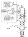
- FIG. 3 shows an effective perimeter defense system 100 that can be made utilizing the sensor architecture discussed above.
- the perimeter defense system 100 utilizes a plurality of parallel sensor rungs 101A-101D to form several perimeter defense sensing zones.
- a transmit/receive module 103 that may be similar to the transmitter/demodulation module 51 provides optical signals to the sensor rungs 101A-101D and also receives optical signals returned from the sensor rungs 101A-101D.
- the sensor rung 101A carries counterpropagating waves such that the optical couplers 105, 113 and 116 and the optical fibers 107, 109 and the sensor rung 101A form a first Sagnac loop 120.
- the clockwise wave and the counter clockwise wave traverse the Sagnac loop 120 and combine in the coupler 105 to form an interference signal that is guided back to the transmit/receive electronics module 103.
- the optical coupler 114 couples a clockwise signal into the sensor rung 101B while the optical coupler 118 couples a counter clockwise signal into the sensor rung 101B.
- the optical couplers 105, 113, 114, 116 and 118 and the optical fibers 107 and 109 and the sensor rung 101B form a second Sagnac loop 122.
- optical couplers 124 and 126 couple clockwise and counter clockwise waves, respectively, into the sensor rung 101C and form a third Sagnac loop 128.
- Optical couplers 130 and 132 couple clockwise and counter clockwise waves, respectively, into the sensor rung 102D and form a fourth Sagnac loop 134.
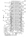
- FIG. 4 shows one such configuration of a perimeter defense system 140 that uses four wavelength bands.
- a linear zone array 141 is formed, where no adjacent sensor zones operate in the same wavelength band. This allows a measure of security should a failure occur upstream in the telemetry system.
- the optical fiber 152 guides signals to a wavelength slicer/demultiplexer 162 that divides the signal output from the transmit/receive demodulator electronics module 146 into four wavelength bands ⁇ 1 , ⁇ 2 , ⁇ 3 and ⁇ 4 to form four counter clockwise waves that are output from the wavelength slicer 162 via optical fibers 165-167, respectively.
- An optical coupler 170 couples signals in the wavelength band ⁇ 1 from the optical fiber 156 into a sensor zone 172A to form a clockwise signal in the wavelength band ⁇ 1 therein.
- an optical coupler 174 couples signals in the wavelength band ⁇ 1 from the optical fiber 164 into the sensor zone 172A to form a counter clockwise signal in the wavelength band ⁇ 1 .
- the clockwise wave in the sensor zone 172A propagates to the optical coupler 174, which couples it into the optical fiber 164.
- the clockwise wave having the wavelength band ⁇ 1 then propagates to the wavelength slicer/demultiplexer 162, which couples it into the optical fiber 152.
- the counter clockwise wave in the sensor zone 172A propagates to the optical coupler 170, which couples it into the optical fiber 156.
- the clockwise wave having the wavelength band ⁇ 1 then propagates to the wavelength slicer/demultiplexer 154, which couples it into the optical fiber 150.
- the clockwise and counter clockwise waves propagate through their corresponding sensor zones 182A, 184A and 186A back to the optical coupler 148.
- the clockwise and counter clockwise waves in each wavelength band combine to form separate interference signals corresponding to each wavelength band. All of the interference signals formed in the optical coupler 148 are input to the transmit/receive demodulator electronics module 146 for processing to determine if any disturbance in any of the sensor zones has produced a change in any of the corresponding interference signals.
- a large number of additional sensor zones may be included in the perimeter defense system 140. Still referring to FIG. 4 , a plurality of optical couplers 200-207 may be used to couple counterpropagating waves into a plurality of sensor zones 172B, 182B, 184B and 186B in the same manner as described above for the sensor zones 172A, 182A, 184A and 186A.
- the sensor zones 172B, 182B, 184B and 186B are included in corresponding Sagnac loops 210-213.
- FIG. 5 illustrates a perimeter defense system 220 that includes a matrix 222 of sensor zones 222A-222P of the type shown in FIG. 4 .
- this perimeter defense system 220 sensor zones operating in the same wavelength band are separated in the horizontal direction of the Figure by a minimum of 2 other wavelength bands.
- the telemetry bus can be designed in such a manner to allow the addition of more zones.
Landscapes
- Physics & Mathematics (AREA)
- General Physics & Mathematics (AREA)
- Gyroscopes (AREA)
- Optical Transform (AREA)
- Instruments For Measurement Of Length By Optical Means (AREA)
- Photometry And Measurement Of Optical Pulse Characteristics (AREA)
- Burglar Alarm Systems (AREA)
- Spectrometry And Color Measurement (AREA)
- Investigating Or Analysing Materials By Optical Means (AREA)
Claims (4)
- Eine Sensor-Anordnung (141, 220) für ein Umkreis-Verteidigungssystem, mit:einer intensitätsmodulierten optischen Breitband-Signalquelle, die zur Erzeugung eines optischen Breitband-Signals angeordnet ist;einem Demultiplexer-/Multiplexer-Paar, das zum Empfang des optischen Breitband-Signals von der optischen Signalquelle und zur Unterteilung dieses Signals in ein getrenntes optisches Signal für jedes einer Vielzahl von Wellenlängen-Bändern angeordnet ist;einem optischen Koppler (148, 226), der zum Empfang der getrennten optischen Signale angeordnet ist;einem ersten Lichtwellenleiter (150) oder einem ersten Teil eines ersten optischen Lichtwellenleiters (228), der mit dem optischen Koppler (148, 226) verbunden und zum Führen einer Uhrzeigersinn-Welle für jedes der getrennten optischen Signale entlang eines entsprechenden optischen Pfades angeordnet ist, und einem zweiten Lichtwellenleiter (152) oder einem zweiten Teil des ersten Lichtwellenleiters (228), der mit dem optischen Koppler (148, 226) verbunden und zum Führen einer Gegenuhrzeigersinn-Welle für jedes der optischen Signale entlang der entsprechenden optischen Pfade angeordnet ist;wobei jeder der entsprechenden optischen Pfade einen jeweiligen weiteren Lichtwellenleiter oder einen jeweiligen ersten Lichtwellenleiter (156 - 159, 234 - 237) und einen jeweiligen zweiten weiteren Lichtwellenleiter (165 - 167, 240 - 243) , der optisch mit den ersten und zweiten Lichtwellenleitern (150, 152) oder mit den ersten und zweiten Teilen des ersten Lichtwellenleiters (228) derart verbunden ist, dass die Uhrzeigersinn- und Gegenuhrzeigersinn-Wellen für das entsprechende eine der getrennten optischen Signale in den weiteren Lichtwellenleiter oder in den ersten weiteren Lichtwellenleiter (156 - 159, 234 - 237) und den zweiten weiteren Lichtwellenleiter (165 - 167, 240 - 243) eigekoppelt werden, und eine jeweilige Vielzahl von Sensoren umfasst, die optisch mit dem weiteren Lichtwellenleiter oder mit dem ersten Lichtwellenleiter (156 - 159, 234 - 237) und dem zweiten weiteren Lichtwellenleiter (165 - 167, 240 - 243) derart gekoppelt sind, dass sich die Uhrzeigersinn- und Gegenuhrzeigersinn-Wellen für das entsprechende eine der getrennten optischen Signale durch die jeweilige Vielzahl von Sensoren ausbreiten und dann in dem optischen Koppler (148, 226) kombiniert werden, um eine Vielzahl von Interferenz-Signalen in dem entsprechenden Wellenlängen-Band zu bilden;einem ersten Demultiplexer, der optisch mit dem optischen Koppler (145, 226) gekoppelt ist, um von diesem Interferenz-Signale zu empfangen;einer ersten Detektor-Anordnung, die zum Empfang der Interferenz-Signale von dem ersten Demultiplexer angeordnet ist, wobei die erste Detektor-Anordnung einen jedem der Vielzahl von Wellenlängen-Bändern entsprechenden Detektor aufweist, der zur Lieferung eines elektrischen Signals angeordnet ist, das die Interferenz-Signale für das entsprechende Wellenlängen-Band anzeigt; undwobei die Sensoren in Sensor-Zonen angeordnet sind, wobei eine Vielzahl von Sensor-Zonen vorhanden ist, die in jedem der Wellenlängen-Bänder arbeiten, und wobei die Sensor-Zonen (172A, 182A, 184A, 186A, 172B, 182B, 184B, 186B, 222A - 222P) derart angeordnet sind, dass keine benachbarten Sensor-Zonen in dem gleichen Wellenlängen-Band arbeiten.
- Die Sensor-Anordnung (141, 220) nach Anspruch 1, bei der der optische Koppler Interferenz-Signale in einen dritten Lichtwellenleiter oder Lichtwellenleiter-Teil einkoppelt, wobei der dritte Lichtwellenleiter oder Lichtwellenleiter-Teil mit dem ersten Demultiplexer verbunden ist, um die Interferenz-Signale an die erste Detektor-Anordnung zu liefern, und bei der der optische Koppler (141, 222) Interferenz-Signale in einen vierten Lichtwellenleiter oder Lichtwellenleiter-Teil einkoppelt, wobei der vierte Lichtwellenleiter oder Lichtwellenleiter-Teil mit einem zweiten Demultiplexer verbunden ist, um Interferenz-Signale an eine zweite Detektor-Anordnung zu liefern.
- Die Sensor-Anordnung (141, 220) nach Anspruch 2, bei der das Demultiplexer-/Multiplexer-Paar zur Unterteilung des optischen Breitband-Signals in optische Signale in ersten bis vierten Wellenlängen-Bändern angeordnet ist, und die Sensor-Anordnung eine lineare Anordnung (141) von Sensor-Zonen (172A, 182A, 184A, 186A, 172B, 182B, 184B, 186B) umfasst.
- Die Sensor-Anordnung (141, 220) nach Anspruch 2, bei der das Demultiplexer-/Multiplexer-Paar zur Unterteilung des optischen Breitband-Signals in optische Bänder in ersten bis vierten Wellenlängen-Bändern angeordnet, und die Sensor-Anordnung eine Matrix (222) von Sensor-Zonen (222A - 222P) umfasst.
Applications Claiming Priority (2)
| Application Number | Priority Date | Filing Date | Title |
|---|---|---|---|
| US11/218,037 US7526147B2 (en) | 2005-08-31 | 2005-08-31 | Sensor array for perimeter defense |
| PCT/US2005/047549 WO2007084110A2 (en) | 2005-08-31 | 2005-12-29 | Sensor array for perimeter deffense |
Publications (2)
| Publication Number | Publication Date |
|---|---|
| EP1934560A2 EP1934560A2 (de) | 2008-06-25 |
| EP1934560B1 true EP1934560B1 (de) | 2014-11-05 |
Family
ID=38288040
Family Applications (1)
| Application Number | Title | Priority Date | Filing Date |
|---|---|---|---|
| EP05858740.3A Expired - Lifetime EP1934560B1 (de) | 2005-08-31 | 2005-12-29 | Sensor-array zur perimeter-verteidigung |
Country Status (5)
| Country | Link |
|---|---|
| US (1) | US7526147B2 (de) |
| EP (1) | EP1934560B1 (de) |
| JP (1) | JP4714270B2 (de) |
| CA (1) | CA2620589C (de) |
| WO (1) | WO2007084110A2 (de) |
Families Citing this family (8)
| Publication number | Priority date | Publication date | Assignee | Title |
|---|---|---|---|---|
| US7526147B2 (en) * | 2005-08-31 | 2009-04-28 | Northrop Grumman, Inc. | Sensor array for perimeter defense |
| US7375817B2 (en) * | 2006-05-15 | 2008-05-20 | Shin-Chu Huang | Counting signal processing method for fiber optic interferometric sensor |
| US8488919B1 (en) * | 2009-01-07 | 2013-07-16 | Alliance Fiber Optic Products, Inc. | Apparatus for combining multiple signals as depolarized output |
| US8345229B2 (en) * | 2009-09-28 | 2013-01-01 | At&T Intellectual Property I, L.P. | Long distance optical fiber sensing system and method |
| PL394318A1 (pl) * | 2011-03-23 | 2012-09-24 | Telekomunikacja Polska Spólka Akcyjna | Uklad do równoczesnego monitorowania wielu wielkosci fizykochemicznych w kilku miejscach srodowiska naturalnego |
| CN103776474A (zh) * | 2014-01-10 | 2014-05-07 | 江苏昂德光电科技有限公司 | 一种3d矩阵式多通道光纤传感解调系统 |
| US10234311B2 (en) * | 2014-10-14 | 2019-03-19 | Halliburton Energy Services, Inc. | Modifying optical signals output by a wavelength division demultiplexer to detect subterranean physical properties |
| US11190271B1 (en) * | 2021-03-04 | 2021-11-30 | Network Integrity Systems, Inc. | Method of monitoring events in an area divided into zones |
Family Cites Families (9)
| Publication number | Priority date | Publication date | Assignee | Title |
|---|---|---|---|---|
| US4770535A (en) * | 1985-02-08 | 1988-09-13 | The Board Of Trustees Of The Leland Stanford Junior University | Distributed sensor array and method using a pulsed signal source |
| WO1999028713A1 (en) * | 1997-12-01 | 1999-06-10 | Geosensor Corporation | Interferometric sensing apparatus |
| US6667935B2 (en) * | 1998-04-03 | 2003-12-23 | The Board Of Trustees Of The Leland Stanford Junior University | Apparatus and method for processing optical signals from two delay coils to increase the dynamic range of a sagnac-based fiber optic sensor array |
| GB9908075D0 (en) * | 1999-04-09 | 1999-06-02 | Secr Defence | An optical fibre sensor assembly |
| KR100305390B1 (ko) * | 1999-05-04 | 2001-09-13 | 윤덕용 | 배열형 사그냑 간섭계 음향센서 및 음향신호 검출방법 |
| US6282334B1 (en) * | 1999-05-13 | 2001-08-28 | Litton Systems, Inc. | Large scale WDM/TDM sensor array employing erbium-doped fiber amplifiers |
| US6445455B1 (en) * | 2000-05-23 | 2002-09-03 | Northrop Grumman Corporation | Phase and intensity modulated IFOG |
| US7305153B2 (en) * | 2005-06-21 | 2007-12-04 | Litton Systems, Inc. | Multi wavelength sensor array |
| US7526147B2 (en) * | 2005-08-31 | 2009-04-28 | Northrop Grumman, Inc. | Sensor array for perimeter defense |
-
2005
- 2005-08-31 US US11/218,037 patent/US7526147B2/en active Active
- 2005-12-29 EP EP05858740.3A patent/EP1934560B1/de not_active Expired - Lifetime
- 2005-12-29 CA CA2620589A patent/CA2620589C/en not_active Expired - Lifetime
- 2005-12-29 WO PCT/US2005/047549 patent/WO2007084110A2/en not_active Ceased
- 2005-12-29 JP JP2008529000A patent/JP4714270B2/ja not_active Expired - Fee Related
Also Published As
| Publication number | Publication date |
|---|---|
| CA2620589A1 (en) | 2007-07-26 |
| WO2007084110A2 (en) | 2007-07-26 |
| EP1934560A2 (de) | 2008-06-25 |
| JP2009506454A (ja) | 2009-02-12 |
| JP4714270B2 (ja) | 2011-06-29 |
| US20070280693A1 (en) | 2007-12-06 |
| US7526147B2 (en) | 2009-04-28 |
| CA2620589C (en) | 2012-03-27 |
| WO2007084110A3 (en) | 2007-11-08 |
Similar Documents
| Publication | Publication Date | Title |
|---|---|---|
| US7154082B2 (en) | Frequency division and/or wavelength division multiplexed recursive fiber optic telemetry scheme for an optical sensor array | |
| AU755607B2 (en) | An optical fibre sensor assembly | |
| EP3543747B1 (de) | Sensorkabel und multiplexes telemetriesystem für seismische kabel mit redundanten/reversiblen optischen verbindungen | |
| US7502120B2 (en) | Fiber optic interferometric sensor array | |
| EP1029222B1 (de) | Verbesserte array-topologie zur benutzung in serien-fiber-bragg-interferometer arrays | |
| CN101715547A (zh) | 地震缆结构 | |
| US8189200B2 (en) | Fiber optic interferometric sensor array with increased multiplexing density | |
| US20090238513A1 (en) | WDM-Based Sensor System And Sensor Interrogation System | |
| EP1934560B1 (de) | Sensor-array zur perimeter-verteidigung | |
| GB2284256A (en) | Wavelength addressed network of fibre optic interferometric sensors | |
| CA2587191A1 (en) | Ocean bottom seismic system | |
| US5140154A (en) | Inline fiber optic sensor arrays with delay elements coupled between sensor units | |
| US5028801A (en) | Apparatus and method for multiplexing fiber optic sensors | |
| JPH04301502A (ja) | 光学検出システムに関する改良 | |
| Cranch et al. | High multiplexing gain using TDM and WDM in interferometric sensor arrays | |
| EP1036307B1 (de) | Interferometrisches detektionsgerät | |
| Peng et al. | Optical fiber hydrophone systems | |
| WO2002073855A8 (de) | Selbstheilende ringstruktur zur optischen nachrichtenübertragung im wellenlängenmultiplex und add/drop-multiplexer hierfür | |
| RU2002122461A (ru) | Акустическая волоконно-оптическая антенна (АВОА) | |
| MXPA06008896A (en) | Frequency division and/or wavelength division multiplexed recursive fiber optic telemetry scheme for an optical sensor array | |
| JPH063639B2 (ja) | 光・音響センサ |
Legal Events
| Date | Code | Title | Description |
|---|---|---|---|
| PUAI | Public reference made under article 153(3) epc to a published international application that has entered the european phase |
Free format text: ORIGINAL CODE: 0009012 |
|
| 17P | Request for examination filed |
Effective date: 20080409 |
|
| AK | Designated contracting states |
Kind code of ref document: A2 Designated state(s): AT DE FR GB IT NL |
|
| 17Q | First examination report despatched |
Effective date: 20080624 |
|
| DAX | Request for extension of the european patent (deleted) | ||
| RBV | Designated contracting states (corrected) |
Designated state(s): AT DE FR GB IT NL |
|
| GRAP | Despatch of communication of intention to grant a patent |
Free format text: ORIGINAL CODE: EPIDOSNIGR1 |
|
| INTG | Intention to grant announced |
Effective date: 20140527 |
|
| GRAS | Grant fee paid |
Free format text: ORIGINAL CODE: EPIDOSNIGR3 |
|
| GRAA | (expected) grant |
Free format text: ORIGINAL CODE: 0009210 |
|
| AK | Designated contracting states |
Kind code of ref document: B1 Designated state(s): AT DE FR GB IT NL |
|
| REG | Reference to a national code |
Ref country code: GB Ref legal event code: FG4D |
|
| REG | Reference to a national code |
Ref country code: AT Ref legal event code: REF Ref document number: 694869 Country of ref document: AT Kind code of ref document: T Effective date: 20141115 |
|
| REG | Reference to a national code |
Ref country code: DE Ref legal event code: R096 Ref document number: 602005045111 Country of ref document: DE Effective date: 20141218 |
|
| REG | Reference to a national code |
Ref country code: NL Ref legal event code: T3 |
|
| REG | Reference to a national code |
Ref country code: AT Ref legal event code: MK05 Ref document number: 694869 Country of ref document: AT Kind code of ref document: T Effective date: 20141105 |
|
| PG25 | Lapsed in a contracting state [announced via postgrant information from national office to epo] |
Ref country code: AT Free format text: LAPSE BECAUSE OF FAILURE TO SUBMIT A TRANSLATION OF THE DESCRIPTION OR TO PAY THE FEE WITHIN THE PRESCRIBED TIME-LIMIT Effective date: 20141105 |
|
| REG | Reference to a national code |
Ref country code: DE Ref legal event code: R097 Ref document number: 602005045111 Country of ref document: DE |
|
| PLBE | No opposition filed within time limit |
Free format text: ORIGINAL CODE: 0009261 |
|
| STAA | Information on the status of an ep patent application or granted ep patent |
Free format text: STATUS: NO OPPOSITION FILED WITHIN TIME LIMIT |
|
| 26N | No opposition filed |
Effective date: 20150806 |
|
| REG | Reference to a national code |
Ref country code: FR Ref legal event code: PLFP Year of fee payment: 11 |
|
| PGFP | Annual fee paid to national office [announced via postgrant information from national office to epo] |
Ref country code: NL Payment date: 20151221 Year of fee payment: 11 |
|
| REG | Reference to a national code |
Ref country code: DE Ref legal event code: R082 Ref document number: 602005045111 Country of ref document: DE Representative=s name: HERNANDEZ, YORCK, DIPL.-ING., DE |
|
| REG | Reference to a national code |
Ref country code: FR Ref legal event code: PLFP Year of fee payment: 12 |
|
| REG | Reference to a national code |
Ref country code: NL Ref legal event code: MM Effective date: 20170101 |
|
| PG25 | Lapsed in a contracting state [announced via postgrant information from national office to epo] |
Ref country code: NL Free format text: LAPSE BECAUSE OF NON-PAYMENT OF DUE FEES Effective date: 20170101 |
|
| REG | Reference to a national code |
Ref country code: FR Ref legal event code: PLFP Year of fee payment: 13 |
|
| P01 | Opt-out of the competence of the unified patent court (upc) registered |
Effective date: 20230607 |
|
| PGFP | Annual fee paid to national office [announced via postgrant information from national office to epo] |
Ref country code: DE Payment date: 20241210 Year of fee payment: 20 |
|
| PGFP | Annual fee paid to national office [announced via postgrant information from national office to epo] |
Ref country code: GB Payment date: 20241224 Year of fee payment: 20 |
|
| PGFP | Annual fee paid to national office [announced via postgrant information from national office to epo] |
Ref country code: FR Payment date: 20241223 Year of fee payment: 20 |
|
| PGFP | Annual fee paid to national office [announced via postgrant information from national office to epo] |
Ref country code: IT Payment date: 20241227 Year of fee payment: 20 |
|
| REG | Reference to a national code |
Ref country code: DE Ref legal event code: R071 Ref document number: 602005045111 Country of ref document: DE |
|
| REG | Reference to a national code |
Ref country code: GB Ref legal event code: PE20 Expiry date: 20251228 |