EP1936427A2 - Procédé de fabrication d'affichage sans interruption - Google Patents
Procédé de fabrication d'affichage sans interruption Download PDFInfo
- Publication number
- EP1936427A2 EP1936427A2 EP07121673A EP07121673A EP1936427A2 EP 1936427 A2 EP1936427 A2 EP 1936427A2 EP 07121673 A EP07121673 A EP 07121673A EP 07121673 A EP07121673 A EP 07121673A EP 1936427 A2 EP1936427 A2 EP 1936427A2
- Authority
- EP
- European Patent Office
- Prior art keywords
- light source
- flat light
- quasi
- panel
- flat
- Prior art date
- Legal status (The legal status is an assumption and is not a legal conclusion. Google has not performed a legal analysis and makes no representation as to the accuracy of the status listed.)
- Withdrawn
Links
- 238000004519 manufacturing process Methods 0.000 title claims abstract description 14
- 239000004973 liquid crystal related substance Substances 0.000 claims abstract description 22
- 239000012788 optical film Substances 0.000 claims abstract description 11
- 239000011159 matrix material Substances 0.000 claims description 28
- 239000010408 film Substances 0.000 claims description 19
- 238000000034 method Methods 0.000 claims description 10
- 230000003287 optical effect Effects 0.000 claims description 6
- 238000005192 partition Methods 0.000 claims description 6
- NIXOWILDQLNWCW-UHFFFAOYSA-N acrylic acid group Chemical group C(C=C)(=O)O NIXOWILDQLNWCW-UHFFFAOYSA-N 0.000 claims description 5
- 239000011521 glass Substances 0.000 claims description 5
- 239000000463 material Substances 0.000 claims description 5
- 238000000465 moulding Methods 0.000 claims description 5
- 238000007747 plating Methods 0.000 claims description 5
- 239000003292 glue Substances 0.000 claims description 4
- 238000010586 diagram Methods 0.000 description 10
- 238000009826 distribution Methods 0.000 description 9
- 238000013461 design Methods 0.000 description 7
- 230000005540 biological transmission Effects 0.000 description 4
- 238000013459 approach Methods 0.000 description 3
- 238000007639 printing Methods 0.000 description 3
- 230000001105 regulatory effect Effects 0.000 description 3
- 238000012937 correction Methods 0.000 description 2
- 230000006872 improvement Effects 0.000 description 2
- 230000002411 adverse Effects 0.000 description 1
- 230000008901 benefit Effects 0.000 description 1
- 230000015572 biosynthetic process Effects 0.000 description 1
- 230000015556 catabolic process Effects 0.000 description 1
- 238000004891 communication Methods 0.000 description 1
- 238000010276 construction Methods 0.000 description 1
- 238000006731 degradation reaction Methods 0.000 description 1
- 238000011161 development Methods 0.000 description 1
- 230000000694 effects Effects 0.000 description 1
- 238000005516 engineering process Methods 0.000 description 1
- 238000001914 filtration Methods 0.000 description 1
- 238000012986 modification Methods 0.000 description 1
- 230000004048 modification Effects 0.000 description 1
- 239000013307 optical fiber Substances 0.000 description 1
- 239000005304 optical glass Substances 0.000 description 1
- 230000004044 response Effects 0.000 description 1
- 238000009827 uniform distribution Methods 0.000 description 1
- 230000000007 visual effect Effects 0.000 description 1
Images


Classifications
-
- G—PHYSICS
- G02—OPTICS
- G02F—OPTICAL DEVICES OR ARRANGEMENTS FOR THE CONTROL OF LIGHT BY MODIFICATION OF THE OPTICAL PROPERTIES OF THE MEDIA OF THE ELEMENTS INVOLVED THEREIN; NON-LINEAR OPTICS; FREQUENCY-CHANGING OF LIGHT; OPTICAL LOGIC ELEMENTS; OPTICAL ANALOGUE/DIGITAL CONVERTERS
- G02F1/00—Devices or arrangements for the control of the intensity, colour, phase, polarisation or direction of light arriving from an independent light source, e.g. switching, gating or modulating; Non-linear optics
- G02F1/01—Devices or arrangements for the control of the intensity, colour, phase, polarisation or direction of light arriving from an independent light source, e.g. switching, gating or modulating; Non-linear optics for the control of the intensity, phase, polarisation or colour
- G02F1/13—Devices or arrangements for the control of the intensity, colour, phase, polarisation or direction of light arriving from an independent light source, e.g. switching, gating or modulating; Non-linear optics for the control of the intensity, phase, polarisation or colour based on liquid crystals, e.g. single liquid crystal display cells
- G02F1/133—Constructional arrangements; Operation of liquid crystal cells; Circuit arrangements
- G02F1/1333—Constructional arrangements; Manufacturing methods
- G02F1/13336—Combining plural substrates to produce large-area displays, e.g. tiled displays
-
- G—PHYSICS
- G02—OPTICS
- G02F—OPTICAL DEVICES OR ARRANGEMENTS FOR THE CONTROL OF LIGHT BY MODIFICATION OF THE OPTICAL PROPERTIES OF THE MEDIA OF THE ELEMENTS INVOLVED THEREIN; NON-LINEAR OPTICS; FREQUENCY-CHANGING OF LIGHT; OPTICAL LOGIC ELEMENTS; OPTICAL ANALOGUE/DIGITAL CONVERTERS
- G02F1/00—Devices or arrangements for the control of the intensity, colour, phase, polarisation or direction of light arriving from an independent light source, e.g. switching, gating or modulating; Non-linear optics
- G02F1/01—Devices or arrangements for the control of the intensity, colour, phase, polarisation or direction of light arriving from an independent light source, e.g. switching, gating or modulating; Non-linear optics for the control of the intensity, phase, polarisation or colour
- G02F1/13—Devices or arrangements for the control of the intensity, colour, phase, polarisation or direction of light arriving from an independent light source, e.g. switching, gating or modulating; Non-linear optics for the control of the intensity, phase, polarisation or colour based on liquid crystals, e.g. single liquid crystal display cells
- G02F1/133—Constructional arrangements; Operation of liquid crystal cells; Circuit arrangements
- G02F1/1333—Constructional arrangements; Manufacturing methods
- G02F1/1335—Structural association of cells with optical devices, e.g. polarisers or reflectors
- G02F1/133504—Diffusing, scattering, diffracting elements
-
- G—PHYSICS
- G02—OPTICS
- G02F—OPTICAL DEVICES OR ARRANGEMENTS FOR THE CONTROL OF LIGHT BY MODIFICATION OF THE OPTICAL PROPERTIES OF THE MEDIA OF THE ELEMENTS INVOLVED THEREIN; NON-LINEAR OPTICS; FREQUENCY-CHANGING OF LIGHT; OPTICAL LOGIC ELEMENTS; OPTICAL ANALOGUE/DIGITAL CONVERTERS
- G02F1/00—Devices or arrangements for the control of the intensity, colour, phase, polarisation or direction of light arriving from an independent light source, e.g. switching, gating or modulating; Non-linear optics
- G02F1/01—Devices or arrangements for the control of the intensity, colour, phase, polarisation or direction of light arriving from an independent light source, e.g. switching, gating or modulating; Non-linear optics for the control of the intensity, phase, polarisation or colour
- G02F1/13—Devices or arrangements for the control of the intensity, colour, phase, polarisation or direction of light arriving from an independent light source, e.g. switching, gating or modulating; Non-linear optics for the control of the intensity, phase, polarisation or colour based on liquid crystals, e.g. single liquid crystal display cells
- G02F1/133—Constructional arrangements; Operation of liquid crystal cells; Circuit arrangements
- G02F1/1333—Constructional arrangements; Manufacturing methods
- G02F1/1335—Structural association of cells with optical devices, e.g. polarisers or reflectors
- G02F1/1336—Illuminating devices
- G02F1/133602—Direct backlight
- G02F1/133603—Direct backlight with LEDs
-
- G—PHYSICS
- G02—OPTICS
- G02F—OPTICAL DEVICES OR ARRANGEMENTS FOR THE CONTROL OF LIGHT BY MODIFICATION OF THE OPTICAL PROPERTIES OF THE MEDIA OF THE ELEMENTS INVOLVED THEREIN; NON-LINEAR OPTICS; FREQUENCY-CHANGING OF LIGHT; OPTICAL LOGIC ELEMENTS; OPTICAL ANALOGUE/DIGITAL CONVERTERS
- G02F1/00—Devices or arrangements for the control of the intensity, colour, phase, polarisation or direction of light arriving from an independent light source, e.g. switching, gating or modulating; Non-linear optics
- G02F1/01—Devices or arrangements for the control of the intensity, colour, phase, polarisation or direction of light arriving from an independent light source, e.g. switching, gating or modulating; Non-linear optics for the control of the intensity, phase, polarisation or colour
- G02F1/13—Devices or arrangements for the control of the intensity, colour, phase, polarisation or direction of light arriving from an independent light source, e.g. switching, gating or modulating; Non-linear optics for the control of the intensity, phase, polarisation or colour based on liquid crystals, e.g. single liquid crystal display cells
- G02F1/133—Constructional arrangements; Operation of liquid crystal cells; Circuit arrangements
- G02F1/1333—Constructional arrangements; Manufacturing methods
- G02F1/1335—Structural association of cells with optical devices, e.g. polarisers or reflectors
- G02F1/1336—Illuminating devices
- G02F1/133602—Direct backlight
- G02F1/133604—Direct backlight with lamps
Definitions
- the present invention relates to a method of manufacturing assembled liquid crystal display, that can be utilized in seamless image displaying large-sized panel.
- the outer edges of the respective panels form visible and evident gaps in an assembled panel, hereby resulting in the partition of screen, and the visually imperfect image presentation.
- the solution of the problem of how to reduce the gaps in an assembled large-sized panel caused by side edges of the constituting panels is essential to achieve high quality image display.
- a light transmission guide that is used to transmit the light of the originally smaller surface of light emitting panel of liquid crystal display or plasma display panel to a larger viewing area, thus eliminating the gap between two adjacent light-emitting panels in a larger-sized assembled panel, hereby forming a visually seamless large-sized display.
- the light transmission guide is required to contain optical fiber or glass tube capable of reflecting the light, and that leads to the high production cost of the light transmission guide; meanwhile, the overall thickness of the assembled display is too much, thus it is inconvenient to assemble and transport.
- the large-sized panel is in great demand for the information and mass communication industries requiring utilization of large-sized panel at reason price.
- the objective of the present invention is to assemble a plurality of smaller LC panels (for example the currently available 26-inch and 32-inch panel) into a larger-sized one at reasonable price, thus achieving almost seamless visual effect of LC panel through a unique optical design on the assembly of the unitary LC panels.
- the objective of the present invention is to disclose a manufacturing method of a seamless display, so that the image signal emitted from LC panel may incident upon and enter into the eyes of a viewer in a direction approximately perpendicular to the protection layer of LC panel, thus avoiding mixing of signals coming from the gaps in an assembled LC panel; meanwhile, the luminance of the image emitted from and near the gaps is enabled to be close to that of the central portion of the various panels assembled, thus creating and maintaining luminance uniformity for various portions in the assembled panel, and achieving the effect and objective of visually seamless image display.
- a further objective of the present invention is to provide a liquid crystal display, including: a backlight unit, an optical film, a partitioned structure, a liquid crystal panel, a protection layer having micro-structures, and a locking portion; thus the LCD display may be assembled through a locking portion thereon and other optical design by making use of more than one unitary panels, hereby forming a visually seamless large-sized display.
- the present invention provides a method for manufacturing seamless display, including the following steps: fixing an light emitting source in a backlight module; fixing an optical film on the light emitting source; placing a partitioned structure on the optical film; aligning or overlapping the side edges of adjacent liquid crystal panels and putting them over the partitioned structure; and providing a protection layer having a micro-structure on the main body of the side edge aligned or overlapped liquid crystal panel, thus forming an LCD display unit.
- the protection layer is made of acrylic or glass material, such that on its surface is formed a prism micro-structure by means of film plating, applying glue film, printing, or molding.
- the light emitting source is a flat light source or quasi-flat light source
- the flat light source is a light emitting diode (LED) or a flat light tube
- the quasi-flat light source is a curve-shaped light tube (for example U-shaped or multi U-shaped light tube).
- light is emitted from the flat light source or quasi-flat light source at a specific angle.
- the specific angle can be varied depending on various conditions, such as size and thickness of the panel, or size of the light box in a backlight module, so as to obtain sufficient supply of light.
- the flat light source or quasi-flat light source is packaged and/or is provided with light cover.
- the flat light source or quasi-flat light source is interleavingly arranged into matrix elements of equal spacing.
- the flat light source or quasi-flat light source further includes a prism film, a diffuser film or a diffuser plate.
- a trapezoidal plate is disposed on a side of the flat light source or quasi-flat light source to form a grid-shaped partitioned structure.
- the light emitted upon being emitted from the flat light source or quasi-flat light source, the light emitted can be made to distribute evenly.
- the light output from the matrix can be controlled through the magnitude of a current.
- each of the respective light emitting diodes in the matrix is arranged to face the perimeter of the panel.
- the positions of the respective rows of light-emitting-diodes in the matrix can be varied.
- At least a ring of light-emitting-diodes can be additionally added to the perimeter of the trapezoidal plate on a side of the quasi-flat light source.
- At least a Cold Cathode Fluorescent Lamp (CCFL) or a Hot Cathode Fluorescent Lamp (HCFL) can be additionally added to each of the respective sides of a trapezoidal plate on a side of the quasi-flat light source.
- CCFL Cold Cathode Fluorescent Lamp
- HCFL Hot Cathode Fluorescent Lamp
- a still further objective of the present invention is to provide a seamless display, including: a backlight module, which includes a plurality of light emitting sources; an optical film; a partitioned structure; a plurality of LCD panels; a protection layer having micro-structures; and a locking portion, hereby forming a display unit; wherein, the side edges of a plurality of liquid crystal panels can be aligned or overlapped, then be used to cover over the partitioned structure.
- the protection layer is made of acrylic or glass material, such that on its surface is formed a prism micro-structure by means of film plating, applying glue film, printing, or molding.
- the light emitting source is a flat light source or quasi-flat light source
- the flat light source is a light emitting diode (LED) or a flat light tube
- the quasi-flat light source is a curve-shaped light tube (for example U-shaped or multi U-shaped light tube).
- the display includes the flat light source or quasi-flat light source is packaged and/or provided with a light cover.
- the display includes the flat light source or quasi-flat light source interleavingly arranged into matrix elements of equal spacing.
- the display includes a prism file, a diffuser film or a diffuser plate.
- the display includes a trapezoidal plate disposed on a side of the flat light source or quasi-flat light source to form a grid-shaped partitioned structure.
- At least a ring of light-emitting-diodes can be additionally added to the perimeter of a trapezoidal plate on a side of the quasi-flat light source.
- At least a Cold Cathode Fluorescent Lamp (CCFL) or a Hot Cathode Fluorescent Lamp (HCFL) can be additionally added to each of the respective sides of a trapezoidal plate on a side of the quasi-flat light source.
- CCFL Cold Cathode Fluorescent Lamp
- HCFL Hot Cathode Fluorescent Lamp
- the present invention discloses a method of manufacturing an assembled panel used for a display, wherein, at least a locking portion is used to bond and connect more than one liquid crystal panels, hereby achieving high and uniform luminance for the entire assembled panel through adjusting the incident angle of light coming from light source, and raising the luminance of gaps between the constituting panels assembled.
- a visually seamless large-sized display that is capable of raising its image display quality remarkably, in addition to reducing its production cost significantly.
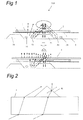
- Fig. 1 is a schematic diagram of a structure of seamless display and the proceeding of an image displaying light according to the present invention
- Fig. 2 is a front view of a micro-structure on a protection layer according to the present invention.
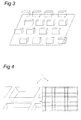
- Fig. 3 is a schematic diagram indicating interleavingly arranging light-emitting-diodes into a matrix of equal spacing members according to the present invention
- Fig. 4 is a schematic diagram indicating a partitioned structure formed by a plurality of trapezoidal plates according to the present invention
- Fig. 5 is a schematic diagram indicating the adjustment of facing angle of the respective row of an LED matrix according to the present invention.
- Fig. 6 is a schematic diagram indicating that the distance between LED's in a matrix and LC panel can be adjusted to achieve even distribution light intensity according to the present invention
- Fig. 7 is a schematic diagram indicating adding light-emitting-diodes to the perimeter of quasi-flat light source according to the present invention.
- Fig. 8 is a schematic diagram indicating adding cold cathode fluorescent lamp (CCFL) and hot cathode fluorescent lamp (HCFL) to the perimeter of quasi-flat light source according to the present invention.
- Fig. 1 is a schematic diagram of a structure of seamless display and the proceeding of an image displaying light according to the present invention.
- display 100 includes a liquid crystal panel 1 and a liquid crystal panel 2, and any one side of liquid crystal panel 1 is aligned or overlapped with any one side of liquid crystal panel 2; an optical film 3, a protection layer 4, and a backlight module 5 (containing light emitting sources 51-54, with its perimeter may further be added trapezoidal plates 71 and 72), and the protection layer 4 is at the outer most layer of the display.
- FIG. 2 is a front view of a micro-structure on a protection layer according to the present invention. Since for an assembled liquid crystal panel in a display, any one side of a unitary panel is made to align or overlap with any one side of another unitary panel, thus the interleaving of obliquely incident lights passing through the gap between adjacent panel tend to create mixing of the image signals, hereby reducing the clearness of the image displayed.
- a necessary correction is performed by a prism micro-structure 41 formed on a surface of a protection layer 4 (made of acrylic or glass material) in the outer most layer of an assembled panel, so that the light emitted from a panel may incident upon and enter into the eyes of a viewer at an angle approximately perpendicular to the protection layer of the panel, hereby avoid mixing of video signals at/near the gaps.
- the protection layer has the functions of both protection and straightening the emitted lights (refer to Fig. 1 ).
- the molding method may also be utilized.
- various optical designs may further be used, so that the light from light source of a display may emit at a certain angle, thus the luminance of the emitted images near the gaps of an assembled panel may close to the luminance at the central portion of the assembled panel, hereby achieving the objective of uniform luminance at various portions of the panel to form a visually seamless display.
- the purpose of the above-mentioned light emitting at a specific angle is only to make sure that lights emitted from light source in a backlight module will not diverge without any restrictions; it will incident upon near the gaps of the assembled panel, so that the luminance of the emitted lights near the gaps will be raised, thus the emission of lights is not restricted strictly to a certain range of angles.
- special design may be made to package the light-emitting-diodes or add special light cover, so as to raise the light luminance at the gaps.
- the light-emitting-diodes may be arranged in an interleaving manner as shown in Fig. 3 to form a matrix of equal spacing members, as such creating a flat light source having special light distribution characteristics, such as light-emitting-diodes of up-and-down interleaving arrangement.
- a prism film, a diffuser film or a diffuser plate may be added in a backlight module.
- a partition structure 7 may be added into a matrix of equally spaced LED's.
- Such partition structure is formed by a plurality of trapezoidal plates (such as 71 and 72 as shown in Fig. 1 ), and that is used to restrict the divergence of light of a light source, so that it may incident upon a panel at a specific angle to form light distribution of higher degree of uniformity.
- the partition structure formed by placing trapezoidal plates into matrix of equally spaced LED's presents a grid-shaped structure (refer to Fig. 4 ).
- flat florescent lamps or curve-shaped lamps (such as U-shaped, multi U-shaped or other curve-shaped lamps) may also be arranged into a matrix, thus making light to incident upon the panel at specific angle by adding trapezoidal plates to restrict the proceeding direction of light.
- the magnitude of a current input to the light source can be regulated, so that the luminance of the edges on both sides of panel can be close to that at the central portion.
- the luminance of the edges on both sides of panel is lower than that at the central portion, thus the magnitude of input current can be regulated to control the matrix, so that light emitted from light source in the perimeter of a matrix is brighter than that from the central portion, as such the intensity of light emitted from the surface of the protection layer may be kept uniform for various parts of the panel after fine tuning.
- the light-emitting-diode is taken as an example.
- the input current to LED's for each row and/or column of a matrix formed by LED's can be regulated, so that light output from LED' s at central portion is smaller than that as output from LED' s at two sides, thus the intensity of light produced by LED's at outer perimeter is stronger than that as produced by LED's at central portion, hereby achieving even more uniform distribution of light intensity and realizing seamless panel of high uniformity of light intensity.
- Fig. 5 is a schematic diagram indicating the adjustment of facing angles of the respective rows and/or columns of an LED matrix according to the present invention.
- a unitary LED on the perimeter of a matrix having higher light intensity than that of a central portion LED is made to face the perimeter of a panel, so that light intensity at that portion is close to that of a central portion of the panel, thus achieving even distribution of light intensity.
- Fig. 6 is a schematic diagram indicating that the distance between LED's in a matrix and LC panel can be adjusted to achieve even distribution light intensity according to the present invention.
- the relative positions of the respective rows of LED's in a matrix can be varied, so that the light intensity of LED's at the edge of a matrix is higher than that at the central portion, hereby realizing even distribution of light intensity.
- flat light tube or curve-shaped light tube for example U-shaped or multi U-shaped light tube
- U-shaped or multi U-shaped light tube may be utilized as the major light source.
- light-emitting-diodes can be added to the perimeter of the quasi-flat light source 67 to enhance the intensity of incident light near the border of adjacent panels, hereby increasing the overall uniformity of luminance of light of an assembled panel.
- a ring or several rings of light-emitting-diodes can be added to the edges of a matrix of multi U-shaped light tubes (such as light-emitting-diodes 51-62 as shown in Fig. 7 ), so that the luminance of light in the perimeter of panel is higher than that in the central portion (in Fig. 7 is shown the overall outlook of a quasi-flat light source, but not the arrangement of multi U-shaped light tubes).
- CCFL Cold Cathode Fluorescent Lamps
- HCFL Hot Cathode Fluorescent Lamps
Landscapes
- Physics & Mathematics (AREA)
- Nonlinear Science (AREA)
- Mathematical Physics (AREA)
- Chemical & Material Sciences (AREA)
- Crystallography & Structural Chemistry (AREA)
- General Physics & Mathematics (AREA)
- Optics & Photonics (AREA)
- Liquid Crystal (AREA)
- Devices For Indicating Variable Information By Combining Individual Elements (AREA)
- Planar Illumination Modules (AREA)
Applications Claiming Priority (1)
| Application Number | Priority Date | Filing Date | Title |
|---|---|---|---|
| CN200610167733XA CN101206327B (zh) | 2006-12-20 | 2006-12-20 | 无接缝显示器及制造无接缝显示器的方法 |
Publications (2)
| Publication Number | Publication Date |
|---|---|
| EP1936427A2 true EP1936427A2 (fr) | 2008-06-25 |
| EP1936427A3 EP1936427A3 (fr) | 2009-08-05 |
Family
ID=39083222
Family Applications (1)
| Application Number | Title | Priority Date | Filing Date |
|---|---|---|---|
| EP07121673A Withdrawn EP1936427A3 (fr) | 2006-12-20 | 2007-11-27 | Procédé de fabrication d'affichage sans interruption |
Country Status (2)
| Country | Link |
|---|---|
| EP (1) | EP1936427A3 (fr) |
| CN (1) | CN101206327B (fr) |
Cited By (3)
| Publication number | Priority date | Publication date | Assignee | Title |
|---|---|---|---|---|
| CN102496356A (zh) * | 2011-12-01 | 2012-06-13 | 广东威创视讯科技股份有限公司 | 一种消除拼接显示屏间拼缝的方法和装置 |
| EP2437103A4 (fr) * | 2009-05-29 | 2014-05-07 | Sharp Kk | Appareil d'affichage et procédé d'affichage |
| EP3246748A4 (fr) * | 2015-01-14 | 2018-10-17 | Boe Technology Group Co. Ltd. | Panneau d'affichage et dispositif d'affichage |
Families Citing this family (16)
| Publication number | Priority date | Publication date | Assignee | Title |
|---|---|---|---|---|
| CN201374154Y (zh) * | 2009-03-20 | 2009-12-30 | 夏展敏 | 消除显示屏拼接框的装置 |
| CN104516136B (zh) * | 2013-09-27 | 2018-09-07 | 鸿富锦精密工业(深圳)有限公司 | 显示装置、拼接式显示器及背光模组 |
| CN103578371B (zh) * | 2013-11-11 | 2016-08-17 | 曹嘉灿 | 无缝液晶显示器及拼装方法 |
| CN104090405B (zh) * | 2014-07-02 | 2017-05-03 | 京东方科技集团股份有限公司 | 一种拼接显示面板及显示装置 |
| US10067369B2 (en) | 2015-11-06 | 2018-09-04 | Champ Vision Display Inc. | Display apparatus with a prism module including a corner prism set disposed on a corner region |
| TWI569237B (zh) | 2015-11-06 | 2017-02-01 | 揚昇照明股份有限公司 | 顯示裝置 |
| TWI567703B (zh) | 2015-11-06 | 2017-01-21 | 揚昇照明股份有限公司 | 顯示裝置 |
| TWI652530B (zh) | 2016-05-04 | 2019-03-01 | 中強光電股份有限公司 | 稜鏡模組以及顯示裝置 |
| TWI611394B (zh) | 2016-08-08 | 2018-01-11 | 誠屏科技股份有限公司 | 多螢幕顯示裝置及其顯示訊號控制方法 |
| CN106200078B (zh) * | 2016-09-05 | 2019-05-07 | 京东方科技集团股份有限公司 | 拼接屏及显示装置 |
| TWM538171U (zh) | 2016-11-11 | 2017-03-11 | 揚昇照明股份有限公司 | 稜鏡組及使用其之顯示裝置 |
| CN107390413B (zh) * | 2017-08-09 | 2020-07-28 | 深圳市华星光电技术有限公司 | 拼接式显示装置及其拼接方法 |
| TWI642050B (zh) | 2017-10-25 | 2018-11-21 | 誠屏科技股份有限公司 | 多螢幕顯示裝置 |
| CN107741670A (zh) * | 2017-11-03 | 2018-02-27 | 惠科股份有限公司 | 一种显示装置及其控制方法 |
| CN107884991A (zh) * | 2017-12-19 | 2018-04-06 | 惠科股份有限公司 | 一种显示装置及其控制方法 |
| TWI760118B (zh) * | 2021-02-24 | 2022-04-01 | 友達光電股份有限公司 | 顯示裝置 |
Citations (1)
| Publication number | Priority date | Publication date | Assignee | Title |
|---|---|---|---|---|
| JP2006047798A (ja) * | 2004-08-06 | 2006-02-16 | Sanyo Electric Co Ltd | 液晶表示装置 |
Family Cites Families (11)
| Publication number | Priority date | Publication date | Assignee | Title |
|---|---|---|---|---|
| JPS56121014A (en) * | 1980-02-28 | 1981-09-22 | Sharp Corp | Liquid-crystal display device |
| US5805117A (en) * | 1994-05-12 | 1998-09-08 | Samsung Electronics Co., Ltd. | Large area tiled modular display system |
| EP1334402A4 (fr) * | 2000-09-19 | 2005-04-06 | Si Han Kim | Dispositif a affichages multiples |
| KR100860982B1 (ko) * | 2002-06-17 | 2008-09-30 | 삼성전자주식회사 | 광경로 이동수단을 가지는 다중표시장치 |
| KR100576865B1 (ko) * | 2004-05-03 | 2006-05-10 | 삼성전기주식회사 | 백라이트용 발광 다이오드 어레이 모듈 및 이를 구비한백라이트 유닛 |
| KR100587373B1 (ko) * | 2004-05-28 | 2006-06-08 | 엘지.필립스 엘시디 주식회사 | 백라이트 유닛 |
| US7901102B2 (en) * | 2004-10-22 | 2011-03-08 | Samsung Electronics Co., Ltd. | Backlight unit and liquid crystal display apparatus employing the same |
| CN100367047C (zh) * | 2004-11-16 | 2008-02-06 | 联想(北京)有限公司 | 一种消除拼接显示屏间拼缝的方法及装置 |
| KR101174770B1 (ko) * | 2005-02-28 | 2012-08-17 | 엘지디스플레이 주식회사 | 백라이트 유닛 및 이를 이용한 액정표시장치 |
| JP4722539B2 (ja) * | 2005-04-27 | 2011-07-13 | 株式会社 日立ディスプレイズ | 表示装置 |
| CN201107507Y (zh) * | 2007-09-14 | 2008-08-27 | 欧睿电通股份有限公司 | 无接缝显示器 |
-
2006
- 2006-12-20 CN CN200610167733XA patent/CN101206327B/zh not_active Expired - Fee Related
-
2007
- 2007-11-27 EP EP07121673A patent/EP1936427A3/fr not_active Withdrawn
Patent Citations (1)
| Publication number | Priority date | Publication date | Assignee | Title |
|---|---|---|---|---|
| JP2006047798A (ja) * | 2004-08-06 | 2006-02-16 | Sanyo Electric Co Ltd | 液晶表示装置 |
Cited By (3)
| Publication number | Priority date | Publication date | Assignee | Title |
|---|---|---|---|---|
| EP2437103A4 (fr) * | 2009-05-29 | 2014-05-07 | Sharp Kk | Appareil d'affichage et procédé d'affichage |
| CN102496356A (zh) * | 2011-12-01 | 2012-06-13 | 广东威创视讯科技股份有限公司 | 一种消除拼接显示屏间拼缝的方法和装置 |
| EP3246748A4 (fr) * | 2015-01-14 | 2018-10-17 | Boe Technology Group Co. Ltd. | Panneau d'affichage et dispositif d'affichage |
Also Published As
| Publication number | Publication date |
|---|---|
| EP1936427A3 (fr) | 2009-08-05 |
| CN101206327A (zh) | 2008-06-25 |
| CN101206327B (zh) | 2011-11-30 |
Similar Documents
| Publication | Publication Date | Title |
|---|---|---|
| US7744289B2 (en) | Seamless display manufacturing method | |
| EP1936427A2 (fr) | Procédé de fabrication d'affichage sans interruption | |
| US8581942B2 (en) | Backlight unit for liquid crystal display device and driving method of the same | |
| TWI772030B (zh) | 指向性背光式顯示裝置 | |
| WO2012036081A1 (fr) | Dispositif d'affichage | |
| WO2009157161A1 (fr) | Dispositif d’affichage et dispositif électronique | |
| JP2010002486A (ja) | 液晶表示装置 | |
| US7742123B2 (en) | Color-filterless LCD | |
| US10698259B2 (en) | Deformed liquid crystal display device | |
| CN201107507Y (zh) | 无接缝显示器 | |
| CN102819139B (zh) | 液晶显示装置 | |
| KR20110064743A (ko) | 백라이트 유닛 및 이를 구비한 액정표시장치 | |
| CN101688649B (zh) | 照明装置、显示装置、电视接收装置 | |
| KR20090128693A (ko) | 액정표시장치 | |
| JP4985154B2 (ja) | 光源装置、表示装置および光学部材 | |
| KR101282289B1 (ko) | 램프가이드 및 이를 포함하는 액정표시장치용 백라이트유닛 | |
| US20140233261A1 (en) | Display device and multi-display device | |
| US7901100B2 (en) | Backlight module unit and backlight module | |
| CN115373174A (zh) | 指向性背光式显示装置 | |
| KR20110024270A (ko) | 백라이트 유닛 및 이를 구비한 액정표시장치 | |
| KR20120020668A (ko) | 복합광학시트 및 이를 포함하는 액정표시장치 | |
| JP2006284906A (ja) | バックライト装置及び液晶表示装置 | |
| KR20060000814A (ko) | 액정표시장치의 백라이트 유닛 | |
| KR20010099170A (ko) | 경사 프리즘 렌즈를 사용한 대화면 평판 표시장치 | |
| KR20100093818A (ko) | 액정표시장치 |
Legal Events
| Date | Code | Title | Description |
|---|---|---|---|
| PUAI | Public reference made under article 153(3) epc to a published international application that has entered the european phase |
Free format text: ORIGINAL CODE: 0009012 |
|
| AK | Designated contracting states |
Kind code of ref document: A2 Designated state(s): AT BE BG CH CY CZ DE DK EE ES FI FR GB GR HU IE IS IT LI LT LU LV MC MT NL PL PT RO SE SI SK TR |
|
| AX | Request for extension of the european patent |
Extension state: AL BA HR MK RS |
|
| PUAL | Search report despatched |
Free format text: ORIGINAL CODE: 0009013 |
|
| AK | Designated contracting states |
Kind code of ref document: A3 Designated state(s): AT BE BG CH CY CZ DE DK EE ES FI FR GB GR HU IE IS IT LI LT LU LV MC MT NL PL PT RO SE SI SK TR |
|
| AX | Request for extension of the european patent |
Extension state: AL BA HR MK RS |
|
| 17P | Request for examination filed |
Effective date: 20100121 |
|
| RAP1 | Party data changed (applicant data changed or rights of an application transferred) |
Owner name: ORIPIX HOLDINGS LIMITED |
|
| RIN1 | Information on inventor provided before grant (corrected) |
Inventor name: HU CHUNG-MING |
|
| AKX | Designation fees paid |
Designated state(s): AT BE BG CH CY CZ DE DK EE ES FI FR GB GR HU IE IS IT LI LT LU LV MC MT NL PL PT RO SE SI SK TR |
|
| 17Q | First examination report despatched |
Effective date: 20100416 |
|
| STAA | Information on the status of an ep patent application or granted ep patent |
Free format text: STATUS: THE APPLICATION IS DEEMED TO BE WITHDRAWN |
|
| 18D | Application deemed to be withdrawn |
Effective date: 20140617 |