EP1936644A2 - Cellule photovoltaïque - Google Patents
Cellule photovoltaïque Download PDFInfo
- Publication number
- EP1936644A2 EP1936644A2 EP07002646A EP07002646A EP1936644A2 EP 1936644 A2 EP1936644 A2 EP 1936644A2 EP 07002646 A EP07002646 A EP 07002646A EP 07002646 A EP07002646 A EP 07002646A EP 1936644 A2 EP1936644 A2 EP 1936644A2
- Authority
- EP
- European Patent Office
- Prior art keywords
- porous
- layer
- electrode
- semiconductor layer
- photovoltaic cell
- Prior art date
- Legal status (The legal status is an assumption and is not a legal conclusion. Google has not performed a legal analysis and makes no representation as to the accuracy of the status listed.)
- Ceased
Links
Images


Classifications
-
- H—ELECTRICITY
- H01—ELECTRIC ELEMENTS
- H01G—CAPACITORS; CAPACITORS, RECTIFIERS, DETECTORS, SWITCHING DEVICES, LIGHT-SENSITIVE OR TEMPERATURE-SENSITIVE DEVICES OF THE ELECTROLYTIC TYPE
- H01G9/00—Electrolytic capacitors, rectifiers, detectors, switching devices, light-sensitive or temperature-sensitive devices; Processes of their manufacture
- H01G9/20—Light-sensitive devices
- H01G9/2027—Light-sensitive devices comprising an oxide semiconductor electrode
- H01G9/2031—Light-sensitive devices comprising an oxide semiconductor electrode comprising titanium oxide, e.g. TiO2
-
- H—ELECTRICITY
- H01—ELECTRIC ELEMENTS
- H01G—CAPACITORS; CAPACITORS, RECTIFIERS, DETECTORS, SWITCHING DEVICES, LIGHT-SENSITIVE OR TEMPERATURE-SENSITIVE DEVICES OF THE ELECTROLYTIC TYPE
- H01G9/00—Electrolytic capacitors, rectifiers, detectors, switching devices, light-sensitive or temperature-sensitive devices; Processes of their manufacture
- H01G9/20—Light-sensitive devices
- H01G9/2022—Light-sensitive devices characterized by he counter electrode
-
- Y—GENERAL TAGGING OF NEW TECHNOLOGICAL DEVELOPMENTS; GENERAL TAGGING OF CROSS-SECTIONAL TECHNOLOGIES SPANNING OVER SEVERAL SECTIONS OF THE IPC; TECHNICAL SUBJECTS COVERED BY FORMER USPC CROSS-REFERENCE ART COLLECTIONS [XRACs] AND DIGESTS
- Y02—TECHNOLOGIES OR APPLICATIONS FOR MITIGATION OR ADAPTATION AGAINST CLIMATE CHANGE
- Y02E—REDUCTION OF GREENHOUSE GAS [GHG] EMISSIONS, RELATED TO ENERGY GENERATION, TRANSMISSION OR DISTRIBUTION
- Y02E10/00—Energy generation through renewable energy sources
- Y02E10/50—Photovoltaic [PV] energy
- Y02E10/542—Dye sensitized solar cells
Definitions
- the present invention relates to a photovoltaic cell, a method of manufacturing such photovoltaic cell, and to uses of such cell.
- Single crystal solar cells show energy conversion efficiencies as high as ⁇ 25%. Where the Si- based crystals are no longer single crystals but polycrystalline, the highest efficiencies are in the range of ⁇ 18%, and with amorphous Si, the efficiencies are ⁇ 12%. Solar cells based on Si are, however, rather expensive to manufacture, even in the amorphous Si version. Therefore alternatives have been developed based on organic compounds and/or a mixture of organic and inorganic compounds, the latter type solar cells often being referred to as hybrid solar cells. Organic and hybrid solar cells have proved to be cheaper to manufacture, but seem to have yet comparably low efficiencies even when compared to amorphous Si cells.
- Photoelectrochemical cells based on sensitisation of nanocrystalline TiO 2 by molecular dyes have attracted great attention since their first announcement as efficient photovoltaic devices (B. O'Regan and M. Grätzel, see above; WO 91/16719 ).
- One part of the ongoing investigations is to exploit the potential applicability of such cells on flexible substrates and with this the potential of fabricating flexible solar cells.
- Dye-sensitized solar cells are based on the photoexcitation of electrons in dye molecules which are attached to semiconductor particles, such as TiO 2 , of a nanoporous network.
- the electrons can be injected into the conduction band of the semiconductor, and if charge recombination is suppressed, the electrons can be collected at one of the electrodes whereas the dye molecules are regenerated from a counter electrode via a charge-conducting agent.
- a matter which was treated so far only sporadically is the separation of the active porous semiconductor layer and the counter electrode.
- the standard approach to solving this problem was so far the use of spacer foils which are made for example from plastic and which are located beside the active porous layer, as can be inspected in figure 1a ).
- an object of the present invention to provide for an improved solar cell that is not as sensitive towards the exertion of pressure on one of the electrodes. Moreover, it was an object of the present invention to provide for an improved solar cell that is not so sensitive towards bending of the electrodes of the solar cell. It was furthermore an object of the present invention to provide for a solar cell that does not show as many short cuts as conventional solar cells constructed in accordance with the prior art.
- a photovoltaic cell comprising a first substrate and a first electrode on said first substrate, preferably in the form of a layer covering said first substrate, more preferably in the form of a layer of a transparent conductive oxide, or, alternatively, a first metal foil acting as a first substrate and a first electrode,
- said porous spacer layer on one side over its entire area is in physical contact with said second electrode, and wherein said porous spacer layer on another side over its entire area is in physical contact with said porous semiconductor layer.
- said porous spacer layer is made of an optically transparent material that is semiconducting or electrically insulating.
- said porous spacer layer has pores with a pore size in the range of from 5 nm to 100 ⁇ m, preferably 5 nm to 1 ⁇ m, more preferably 5 nm to 500 nm, and most preferably 10 nm to 100 nm.
- said porous spacer layer is a foil having pores with an average diameter in the range of from 10 nm to 100 ⁇ m, preferably from 10 nm to 1 ⁇ m.
- said porous spacer layer is made from particles having sizes in the range of from 1 nm to ⁇ 1 ⁇ m, preferably from 1 nm to 500 nm, more preferably from 1 nm to 300 nm, even more preferably from 1 nm to 200 nm and most preferably from 10 nm to 100 nm.
- said particles are semiconductor particles or insulator particles, wherein, preferably, said semiconductor or insulator particles are made of a material or a combination of materials, selected from TiO 2 , SnO 2 , Sb 2 O 5 , CdTe, CdSe, CdS, ZnO, Nb 2 O 5 , ZrO 2 , CeO 2 , WO 3 , SiO 2 , Al 2 O 3 , CuAlO 2 , SrTiO 3 , SrCu 2 O 2 , SiO 2 , (preferably silica or glass beads), heat resistant polymers, such as crosslinked silicone resin, crosslinked polystyrene, crosslinked acrylic resin, melamine-formaldehyde resin, aromatic polyamide resin, polyimide resin, polyamide-imide resin, crosslinked polyesters, metal carbonates, such as magnesium carbonate, calcium carbonate, metal sulfates, such as calcium sulfate, barium sulfate.
- said porous semiconductor layer is dye-sensitized and said porous spacer layer is not dye-sensitized.
- said porous spacer layer covers said porous semiconductor layer over the entire area of said porous semiconductor layer and thereby electrically insulates said porous semiconductor layer from said second electrode.
- said cell does not comprise any spacer entities, such as spacer foils, arranged between said first and said second electrode, that electrically insulate said porous semiconductor layer from said second electrode and that are located beside said porous semiconductor layer.
- spacer entities such as spacer foils
- said cell comprises said porous spacer layer as the only spacer entity to electrically insulate said porous semiconductor layer from said second electrode.
- said porous spacer layer has a pore size distribution or monodisperse pore size in the range of from 5 nm to 100 ⁇ m, preferably from 5 nm to 1 ⁇ m, more preferably from 5 nm to 500 nm, and most preferably from 10 nm to 100 nm.
- said particles of said porous spacer layer have a particle size distribution or monodisperse pore size in the range of from 1 nm to ⁇ 1 ⁇ m, preferably from 1 nm to 500 nm, more preferably from 1 nm to 300 nm, even more preferably from 1 nm to 200 nm, and most preferably from 10 nm to 100 nm.
- said porous spacer layer has a thickness in the range of from 100 nm to 100 ⁇ m, preferably from 1 ⁇ m to 10 ⁇ m.
- said porous spacer layer covers parts of the area of said porous semiconductor layer and does not cover other parts of the area of said porous semiconductor layer, and wherein the covered area of said porous semiconductor layer is > 50% of the entire area of said porous semiconductor layer.
- a ratio between gap size and pore size is in the range of from 1 to 1000, preferably from 10 to 100.
- said porous spacer layer is produced via a method selected from screen printing, doctor blading, ink-jet-printing, drop-casting, spin coating, spraying, electrostatic layer-by-layer self-assembly, lift-off process, mineralization, and anodic oxidation.
- a first metal foil is used instead of said first substrate and said first electrode together, and wherein said second electrode is a semitransparent metal layer, e.g. a semitransparent Pt layer, and wherein said cell comprises said second substrate which is a transparent substrate, and wherein between said second substrate and said second electrode, optionally there is a transparent conductive oxide.
- said second electrode is a semitransparent metal layer, e.g. a semitransparent Pt layer
- said cell comprises said second substrate which is a transparent substrate, and wherein between said second substrate and said second electrode, optionally there is a transparent conductive oxide.
- the objects of the present invention are also solved by the use of a porous spacer layer in a photovoltaic cell for preventing short circuiting between a photoactive semiconductor layer and a counter electrode of said cell, and/or for insulating a photoactive semiconductor layer and a counter electrode of said cell from each other, wherein said porous spacer layer is as defined above.
- active layer is meant to refer to a layer within a photovoltaic cell that is involved in light absorption, charge separation and charge transfer processes.
- photoactive is a photoactive porous layer, more specifically a photoactive porous semiconductor layer.
- an electrode is referred to as being "in physical contact with" a layer, if the electrode with one of its faces touches the layer.
- this term is meant to refer to an electrode that takes the shape of a layer itself, for example a layer of transparent conductive oxide or a layer of metal, which layer with one of its surfaces touches and is situated upon the other layer, for example a porous spacer layer. In essence, such arrangement can be described as a laminate of two layers on top of each other.
- the electrode e.g. the first or second electrode, may also be a metal foil.
- interstitial space as used herein, is meant to refer to the space created and formed by the pores within a porous layer.
- the interstitial space is essentially a network of pores that are linked together.
- Two interstitial spaces are referred to herein as being "in fluid connection with” each other, if fluid, such as gas or liquid, present in one interstitial space can move into the other interstitial space without a physical barrier between the two interstitial spaces. That is to say the two interstitial spaces are in communication with each other, and the movement of a chemical species within the interstitial spaces, e.g. of a solvent molecule or of an electrolyte, is only limited by diffusion and not by any solid physical barriers.
- a void volume of electrolyte is meant to refer to any bulk volume taken up by electrolyte which is not interstitial space.
- gap size is meant to refer to the distance of the surface of the photoactive porous layer to the counter electrode (see, for example, figure 1a ) and b).
- the photoactive porous layer or photoactive porous semiconductor layer may be considered as forming a part of the photoactive electrode.
- the term "sintering" when used in connection with a porous particle layer is meant to refer to a heat treatment step of for example a semiconductor particle layer in the course of which one or several of the following processes take place: An increase of particle contact by formation of sinter-bridges, formation of a porous network in which the original particles may not necessarily be identifiable anymore, and further smoothening of the pores.
- any sintering process in accordance with the present invention when applied to a semiconductor layer involves temperatures > 300°C.
- “Sintering” is to be contrasted to “drying", as used herein, of a semiconductor layer. Such “drying” mainly involves the elimination of any liquid components or materials / solids with low boiling temperature previously present in the semiconductor layer, such as, for example, solvent. Usually, such “drying” occurs at temperatures ⁇ 250°C.
- the porous spacer layer creates an electrically insulating barrier between the counter electrode and the first electrode or the photoactive layer, whilst at the same time the porous spacer layer is in direct contact with the counter electrode and thereby does not allow the formation of bulk volume or gap volume that would lie between the porous spacer layer and the counter electrode, as such gap volume would, again, make the resulting cell pressure sensitive towards the exertion of pressure on the counter electrode or front electrode.
- an "entire area” of a layer that is covered or contacted by another layer is meant to refer to the area of a fictitious plane parallel to and on the surface of such layer at which the contact occurs.
- the layer is treated as if it had a smooth plane as a surface, and it is the area of such smooth plane to which the term “entire area” refers. If only “parts” or a “part” of "the entire area” is covered or contacted, this usually refers to a proportion of the area of such fictitious plane.
- the covered area of said porous semiconductor layer is > 50% of the entire area of the porous semiconductor layer
- the phrase “entire area” or “area” usually refers to the area of such fictitious plane, and not to the actual surface area of the porous semiconductor layer/porous spacer layer which may have a much larger surface area because of its particulate character.
- heat resistant polymer is meant to refer to a polymer which remains dimensionally stable under the influence of heat. Preferably, it refers to a polymer that remains dimensionally stable in a temperature range of the operating temperatures of a photovoltaic cell. More preferably, a "heat resistant polymer” is a polymer that remains dimensionally stable in a temperature range up to and including 80°C.
- particles that have sizes in the range of from 1 nm to ⁇ 1 ⁇ m are also sometimes referred to as “nanoparticles”.
- the semiconductor or insulator particles of the porous spacer layer may be made of any of the aforementioned semiconductor or insulator materials, or of a combination of any of the aforementioned materials. Likewise, there may be more than one kind of particles in the sense that there may be different particles each made of a different semiconductor or insulator material or those with a core shell structure. Such core shell structures of nanoparticles are known to someone skilled in the art.
- step C) involves the sandwiching of the products of steps A) and B).
- sandwiching is known to someone skilled in the art and is for example achieved by putting the two products in physical contact with each other and holding them together by e.g. clamping or sealing them together with e.g. glue or glass seal.
- a photovoltaic cell that is dye-sensitized, as used herein, is also sometimes referred to as a dye-sensitized solar cell (DSSC).
- DSSC dye-sensitized solar cell
- Substrates that may be used in accordance with the present invention are transparent substrates, such as glass, plastic, e.g. polymethylmethacrylate (PMMA) and others. Substrates may be rigid or flexible. It is clear to someone skilled in the art that there exists a wide variety of flexible substrates.
- flexible substrates may be used, such as but not limited thereto: polyethylene terephthalate (PET), polyethylene naphthalate (PEN), polyethersulphone (PES), polymethylmethacrylate (PMMA), polyimide (kapton), polyetheretherketone (PEEK), polyetherimide (PEI), OHP (overhead transparencies), metal foils like Ti-foil, Pt-foil, Al-foil, stainless steel.
- Electrodes useful in accordance with the present invention are metal electrodes that have been applied as a layer on the substrate, and/or transparent conductive oxides (TCO), such as conductive ITO (Indium tin oxide) or FTO (fluorine tin oxide) or ATO (antimony tin oxide) or zinc oxide (ZnO).
- TCO transparent conductive oxides
- ITO Indium tin oxide
- FTO fluorine tin oxide
- ATO antimony tin oxide
- ZnO zinc oxide
- the one or the other substrate and the electrode layer applied thereon can be replaced by a metal foil which has enough rigidity to function as a supporting substrate as well as the required conductivity.
- the flexible solar cell is a dye-sensitized solar cell illuminated from the back
- the front electrode and substrate is formed by the aforementioned metal foil
- the other electrode is formed by a semi-transparent metal layer, such as Pt alone or in combination with a transparent conductive oxide, on top of which an additional transparent substrate is placed.
- a schematic diagram of such backside illuminated DSSC is shown in figure 4 .
- porous layers such as porous semiconductor layers on substrates or electrodes
- screen-printing doctor blading
- ink-jet printing drop casting
- spin coating spin coating
- spraying layer-by-layer-assembly
- lift-off-processes lift-off-processes and anodic oxidation all of which are well known to a person skilled in the art.
- the "porous semiconductor layer which is a photoactive layer” as used herein, is a layer of semiconductor particles which is involved in light absorption, charge separation and charge transfer processes. Usually, it is made from semiconductor particles which are made of a material or a combination of materials known to persons skilled in the art. It is clear to someone skilled in that art that a wide variety of semiconductor particles can be used for producing such a photoactive porous semiconductor layer.
- Examples of such material are, without being limited thereto: TiO 2 , SnO 2 , Sb 2 O 5 , CdTe, CdSe, CdS, ZnO, Nb 2 O 5 , ZrO 2 , CeO 2 , WO 3 , SiO 2 , Al 2 O 3 , CuAlO 2 , SrTiO 3 and SrCu 2 O 2 .
- the inventors have surprisingly found that by avoiding the conventional prior art spacer foils, effectively, the photoactive area available for charge separation and transfer processes can be enlarged whilst at the same time, the frequency of short circuiting is decreased.
- This is achieved in accordance with the present invention by the presence of a porous spacer layer that is not a photoactive layer which acts as an insulator and/or separator of the photoactive layer and the counter electrode.
- the inventors have found that the use of such a porous spacer layer has the advantage of a lower probability of short circuiting of the dye-sensitized solar cell during operation.
- Fig. 1 (b) The general concept is sketched in Fig. 1 (b) . It makes use of a material which (i) ensures electrical separation between the photoactive porous layer and the counter electrode over the whole area of the active porous layer or a major part thereof and/or the whole area of the counter electrode or a major part thereof and (ii) enables the ions in the electrolyte to move freely between the photoactive porous layer and the counter electrode.
- a porous material with channels which fills completely or a major part of the gap between the 2 electrodes (i.e. the area between the surfaces of the photoactive layer and the counter electrode.
- the pore size has to be in the order of the gap size or smaller between the two electrodes. If, e.g., the distance between the single channels was larger than the diffusion path across the gap, this additional distance could negatively influence the cell performance, especially it could lead to diffusion limitations to the short current density and fill factor of the cell.
- Nanoporous TiO 2 is normally sintered at temperatures above 400 °C to ensure good electrical contact between the single particles.
- this TiO 2 layer can be brought into direct contact with the active porous layer and no electrical current will flow via the porous material between the active porous layer and the counter electrode.
- organic material is normally added to the nanoparticles.
- the voids left behind after burning the organic material at high temperatures then determine the porosity of the porous layer.
- an organic-free suspension of TiO 2 may be used and the porosity is solely adjusted by the particle size and degree of aggregation of the nanoparticles without high sintering temperatures.
- TiO 2 a TiO 2 suspension was synthesized as follows: Titanium(IV)isopropoxide is reacted with the same molar amount of acetic acid. A white solid precipitates after adding water. It is redispersed and nitric acid is added to the solution. The solution is heated to complete the peptisation. Hydrothermal synthesis is then carried out in a sealed titanium pressure vessel at 190 °C for 6 hours. Ultrasonic bath treatment, adjustment of TiO 2 content, and the addition of 1-propanol and ethanol then complete the synthesis.
- a DSSC with porous spacer was assembled as follows: A 30-nm-thick bulk TiO 2 blocking layer is formed on FTO (approx. 100 nm on glass). A 10- ⁇ m-thick porous layer of semiconductor particles is screen printed on the blocking layer and sintered at 450 °C for half an hour. Red dye molecules (N3 bis-TBA) were adsorbed to the particles via self-assembling out of a solution in ethanol (0.3 mM) and the porous layer was filled with electrolyte containing I - /I 3 - as redox couple (15 mM). A porous TiO 2 spacer layer was applied on a reflective platinum back electrode by means of doctor blading a water based TiO 2 suspension. The porous spacer layer was dried at 150 °C and had a resulting thickness of about 5 ⁇ m. This counter electrode was also filled with the above-described electrolyte and was then directly sandwiched onto the active porous layer.
- a further advantage is that the optical properties of the nanoporous TiO 2 can be adjusted by the particle size and the degree of aggregation. Low aggregation and small particle size lead to transparent films. In the case of backside-illuminated DSSC, a transparent porous spacer layer is of increased advantage ( Fig. 4 ).
- a DSSC with porous spacer was assembled as follows: blocking layer, porous layer as well as dye adsorption were prepared following the same procedure as described in example 1.
- the porous layer was penetrated by a polymer gel electrolyte based on a mixture of polyethylene oxide (3 wt%), propylene carbonate and ethylene carbonate with I - 3 /I - as the redox couple; the I - 3 concentration was 15mM and the ratio of propylene carbonate to ethylene carbonate was equal to one.
- a porous TiO 2 spacer layer was applied on a reflective platinum back electrode by means of doctor blading a water based TiO 2 suspension. The porous spacer layer was dried at 150 °C and had a resulting thickness of about 2 ⁇ m.
- This counter electrode was also filled with the above-described electrolyte and was then directly sandwiched onto the active porous layer. As a standard spacer, a 2 ⁇ m thick foil was used.
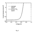
- Figure 6 shows the J-V-characteristics of cells with standard spacers, cells in which the photoactive porous layer are partly covered by spacer foil and cells in accordance with the present invention using a porous spacer layer.
- Figure 7 shows the photovoltaic parameters of a cell using spacer foils, a cell in which the photoactive porous layer is partly covered by spacer foil and a cell in accordance with the present invention.
Landscapes
- Engineering & Computer Science (AREA)
- Power Engineering (AREA)
- Microelectronics & Electronic Packaging (AREA)
- Hybrid Cells (AREA)
- Photovoltaic Devices (AREA)
Priority Applications (4)
| Application Number | Priority Date | Filing Date | Title |
|---|---|---|---|
| EP07002646A EP1936644A3 (fr) | 2006-12-22 | 2007-02-07 | Cellule photovoltaïque |
| JP2007330847A JP2008192603A (ja) | 2006-12-22 | 2007-12-21 | 光電池 |
| US11/963,090 US8193443B2 (en) | 2006-12-22 | 2007-12-21 | Photovoltaic cell |
| AU2007254620A AU2007254620B2 (en) | 2006-12-22 | 2007-12-21 | A photovoltaic cell |
Applications Claiming Priority (2)
| Application Number | Priority Date | Filing Date | Title |
|---|---|---|---|
| EP06026773 | 2006-12-22 | ||
| EP07002646A EP1936644A3 (fr) | 2006-12-22 | 2007-02-07 | Cellule photovoltaïque |
Publications (2)
| Publication Number | Publication Date |
|---|---|
| EP1936644A2 true EP1936644A2 (fr) | 2008-06-25 |
| EP1936644A3 EP1936644A3 (fr) | 2011-01-05 |
Family
ID=39305328
Family Applications (1)
| Application Number | Title | Priority Date | Filing Date |
|---|---|---|---|
| EP07002646A Ceased EP1936644A3 (fr) | 2006-12-22 | 2007-02-07 | Cellule photovoltaïque |
Country Status (4)
| Country | Link |
|---|---|
| US (1) | US8193443B2 (fr) |
| EP (1) | EP1936644A3 (fr) |
| JP (1) | JP2008192603A (fr) |
| AU (1) | AU2007254620B2 (fr) |
Cited By (21)
| Publication number | Priority date | Publication date | Assignee | Title |
|---|---|---|---|---|
| GB2462700A (en) * | 2008-07-08 | 2010-02-24 | Honeywell Int Inc | Solar cell with a porous insulating layer |
| WO2010091278A3 (fr) * | 2009-02-05 | 2011-05-12 | The Research Foundation Of State University Of New York | Cellule de conversion d'énergie comportant une région à graduation diélectrique pour modifier le transport, et procédés associés |
| WO2011110869A3 (fr) * | 2010-03-11 | 2011-11-03 | Isis Innovation Limited | Dispositif d'hétérojonction photosensible à semi-conducteur |
| US8067763B2 (en) | 2007-12-19 | 2011-11-29 | Honeywell International Inc. | Quantum dot solar cell with conjugated bridge molecule |
| US8089063B2 (en) | 2007-12-19 | 2012-01-03 | Honeywell International Inc. | Quantum dot solar cell with electron rich anchor group |
| US8106388B2 (en) | 2007-12-19 | 2012-01-31 | Honeywell International Inc. | Quantum dot solar cell with rigid bridge molecule |
| US8148632B2 (en) | 2008-07-15 | 2012-04-03 | Honeywell International Inc. | Quantum dot solar cell |
| US8227687B2 (en) | 2009-02-04 | 2012-07-24 | Honeywell International Inc. | Quantum dot solar cell |
| US8227686B2 (en) | 2009-02-04 | 2012-07-24 | Honeywell International Inc. | Quantum dot solar cell |
| FR2972841A1 (fr) * | 2011-03-17 | 2012-09-21 | Saint Gobain | Cellule photovoltaique a colorant et son procede de fabrication |
| US8283561B2 (en) | 2008-05-13 | 2012-10-09 | Honeywell International Inc. | Quantum dot solar cell |
| US8288649B2 (en) | 2008-02-26 | 2012-10-16 | Honeywell International Inc. | Quantum dot solar cell |
| US8299355B2 (en) | 2008-04-22 | 2012-10-30 | Honeywell International Inc. | Quantum dot solar cell |
| US8373063B2 (en) | 2008-04-22 | 2013-02-12 | Honeywell International Inc. | Quantum dot solar cell |
| US8372678B2 (en) | 2009-12-21 | 2013-02-12 | Honeywell International Inc. | Counter electrode for solar cell |
| US8426728B2 (en) | 2009-06-12 | 2013-04-23 | Honeywell International Inc. | Quantum dot solar cells |
| US8455757B2 (en) | 2008-08-20 | 2013-06-04 | Honeywell International Inc. | Solar cell with electron inhibiting layer |
| US8710354B2 (en) | 2007-12-19 | 2014-04-29 | Honeywell International Inc. | Solar cell with hyperpolarizable absorber |
| US8771556B2 (en) | 2010-11-05 | 2014-07-08 | Hyundai Motor Company | Semiconductor oxide ink composition for inkjet printing, method of manufacturing the same, and method of manufacturing photoelectric conversion element using the same |
| CN108475582A (zh) * | 2016-01-06 | 2018-08-31 | 国际先端技术综合研究所株式会社 | 光发电元件 |
| CN111662550A (zh) * | 2019-03-07 | 2020-09-15 | 宁德时代新能源科技股份有限公司 | 导热硅胶组合物、导热硅胶材料及制备方法 |
Families Citing this family (29)
| Publication number | Priority date | Publication date | Assignee | Title |
|---|---|---|---|---|
| EP1933343A1 (fr) * | 2006-12-13 | 2008-06-18 | Sony Deutschland Gmbh | Méthode de production d'un film semiconductor poreux sur un substrat |
| JP5135520B2 (ja) * | 2007-06-26 | 2013-02-06 | 国立大学法人九州工業大学 | 色素増感太陽電池 |
| JP5273709B2 (ja) * | 2008-07-02 | 2013-08-28 | シャープ株式会社 | 色素増感太陽電池、その製造方法および色素増感太陽電池モジュール |
| JP4683396B2 (ja) * | 2009-04-30 | 2011-05-18 | シャープ株式会社 | 多孔質電極、色素増感太陽電池、および色素増感太陽電池モジュール |
| GB0909818D0 (en) * | 2009-06-08 | 2009-07-22 | Isis Innovation | Device |
| KR20110016072A (ko) * | 2009-08-11 | 2011-02-17 | 주식회사 동진쎄미켐 | 염료감응 태양전지 및 이로부터 구성되는 모듈 |
| KR101074577B1 (ko) | 2009-09-29 | 2011-10-17 | 재단법인대구경북과학기술원 | 유무기 하이브리드 태양전지 및 이의 제조방법 |
| JP4935910B2 (ja) * | 2010-01-07 | 2012-05-23 | 大日本印刷株式会社 | 有機薄膜太陽電池 |
| TWI396292B (zh) * | 2010-01-11 | 2013-05-11 | Tatung Co | 太陽能電池及其製造方法 |
| JP4858652B2 (ja) * | 2010-03-30 | 2012-01-18 | 大日本印刷株式会社 | 色素増感型太陽電池 |
| KR101112701B1 (ko) | 2010-04-27 | 2012-02-16 | 주식회사 엘 앤 에프 | 금속염과 금속탄산염이 도입된 유무기 하이브리드 태양전지 및 그 제조방법 |
| US20110220192A1 (en) * | 2010-05-23 | 2011-09-15 | Fariba Tajabadi | Single-sided dye-sensitized solar cells having a vertical patterned structure |
| US20130255761A1 (en) * | 2010-06-17 | 2013-10-03 | Polymers Crc Ltd. | Electrode and dye-sensitized solar cell |
| JP2012113942A (ja) * | 2010-11-24 | 2012-06-14 | Ricoh Co Ltd | 多層型光電変換素子およびその製造方法 |
| KR101234239B1 (ko) * | 2011-01-21 | 2013-02-18 | 삼성에스디아이 주식회사 | 염료감응 태양전지 및 그 제조방법 |
| CN102237200B (zh) * | 2011-03-04 | 2013-04-17 | 中国科学院物理研究所 | 用于敏化太阳能电池的金属硫化物对电极及其制备方法 |
| TWI542023B (zh) * | 2011-03-11 | 2016-07-11 | Internat Frontier Tech Lab Inc | Silicon dioxide solar cells |
| WO2013077209A1 (fr) * | 2011-11-21 | 2013-05-30 | シャープ株式会社 | Cellule photovoltaïque liquide ainsi que module de cellules photovoltaïques liquides |
| JP2013196948A (ja) * | 2012-03-21 | 2013-09-30 | Osaka Gas Co Ltd | 正極セパレータ一体型電極及び光電変換素子 |
| JP6032915B2 (ja) * | 2012-03-29 | 2016-11-30 | 大阪瓦斯株式会社 | 光電変換素子用多孔質酸化物半導体層及びその製造方法 |
| JP2013232362A (ja) * | 2012-05-01 | 2013-11-14 | Sharp Corp | 光電変換素子および光電変換モジュール |
| US10121601B2 (en) | 2012-05-22 | 2018-11-06 | International Frontier Technology Laboratory, Inc. | Photoelectrode material and photocell material |
| JP2014017238A (ja) * | 2012-06-11 | 2014-01-30 | Rohm Co Ltd | 色素増感太陽電池およびその製造方法 |
| TWI578555B (zh) * | 2012-09-18 | 2017-04-11 | 學校法人東京理科大學 | 色素增感太陽能電池 |
| EP2913883A4 (fr) * | 2012-10-23 | 2015-10-14 | Univ Tokyo Sci Educ Found | Photoélectrode destinée à des cellules solaires à colorant, et cellule solaire à colorant |
| US9947884B1 (en) * | 2013-04-22 | 2018-04-17 | Pison Stream Solutions, Llc | Solar active powder for fusion powder coating |
| WO2015129608A1 (fr) * | 2014-02-26 | 2015-09-03 | 住友大阪セメント株式会社 | Pâte pour couche isolante poreuse réfléchissant la lumière, couche isolante poreuse réfléchissant la lumière et cellule solaire à colorant |
| CN105895736B (zh) * | 2016-03-15 | 2017-06-23 | 深圳市金耀辉科技有限公司 | 一种耐高温柔性衬底微晶硅薄膜的制备方法 |
| JP2018152411A (ja) * | 2017-03-10 | 2018-09-27 | 株式会社フジコー | バックコンタクト型ペロブスカイト光電変換素子 |
Citations (1)
| Publication number | Priority date | Publication date | Assignee | Title |
|---|---|---|---|---|
| US20040112422A1 (en) * | 2002-12-11 | 2004-06-17 | Spivack James L. | Structured micro-channel semiconductor electrode for photovoltaic cells |
Family Cites Families (21)
| Publication number | Priority date | Publication date | Assignee | Title |
|---|---|---|---|---|
| WO1997016838A1 (fr) * | 1995-10-31 | 1997-05-09 | Ecole Polytechnique Federale De Lausanne | Accumulateur a cellules photovoltaiques et son procede de fabrication |
| KR19980031200A (ko) * | 1996-10-31 | 1998-07-25 | 배순훈 | 브이씨알(vcr)의 화면 탐색 방법 |
| JP2000294306A (ja) * | 1999-04-06 | 2000-10-20 | Fuji Photo Film Co Ltd | 光電変換素子および光電気化学電池 |
| US6291763B1 (en) * | 1999-04-06 | 2001-09-18 | Fuji Photo Film Co., Ltd. | Photoelectric conversion device and photo cell |
| JP2001102104A (ja) * | 1999-09-30 | 2001-04-13 | Fuji Photo Film Co Ltd | 光電変換素子および光電池 |
| JP4738559B2 (ja) * | 1999-09-29 | 2011-08-03 | 日揮触媒化成株式会社 | 光電気セル |
| JP2001357897A (ja) * | 2000-06-14 | 2001-12-26 | Fuji Xerox Co Ltd | 光電変換モジュール |
| JP4100863B2 (ja) * | 2000-10-23 | 2008-06-11 | 触媒化成工業株式会社 | 光電気セル |
| JP4461656B2 (ja) * | 2000-12-07 | 2010-05-12 | セイコーエプソン株式会社 | 光電変換素子 |
| EP1463073A1 (fr) | 2003-03-24 | 2004-09-29 | Sony International (Europe) GmbH | Film poreux ayant un gradient de la diffusion de la lumière |
| EP1513171A1 (fr) | 2003-09-05 | 2005-03-09 | Sony International (Europe) GmbH | Cellule solaire sensibilisé par un colorant et méthode pour sa fabrication |
| JP2005093406A (ja) * | 2003-09-17 | 2005-04-07 | Kuramoto Ryuji | 光電変換素子およびその光電変換効率を向上する方法 |
| JP4601285B2 (ja) * | 2003-11-07 | 2010-12-22 | 大日本印刷株式会社 | 色素増感型太陽電池用電極基板及びその製造方法並びに色素増感型太陽電池 |
| WO2005083730A1 (fr) * | 2004-02-19 | 2005-09-09 | Konarka Technologies, Inc. | Cellule photovoltaïque dotée d'entretoises |
| JP2005268107A (ja) * | 2004-03-19 | 2005-09-29 | Mitsubishi Electric Corp | 色素増感型太陽電池とその製造方法 |
| EP1589548A1 (fr) | 2004-04-23 | 2005-10-26 | Sony Deutschland GmbH | Méthode de production d'un film semiconducteur poreux sur un substrat. |
| CN100481521C (zh) | 2004-07-08 | 2009-04-22 | 住友化学株式会社 | 多孔电极、包含该多孔电极的设备及其制备方法 |
| JP4836473B2 (ja) * | 2005-03-23 | 2011-12-14 | 京セラ株式会社 | 光電変換装置およびその製造方法ならびに光発電装置 |
| JP4856079B2 (ja) * | 2005-09-02 | 2012-01-18 | 京セラ株式会社 | 光電変換装置及びその製造方法並びに光発電装置 |
| WO2007043533A1 (fr) * | 2005-10-11 | 2007-04-19 | Kyocera Corporation | Transducteur photoélectrique, processus de fabrication idoine, et appareil photovoltaique |
| KR100659831B1 (ko) * | 2005-10-19 | 2006-12-19 | 삼성전자주식회사 | 염료감응형 태양 전지 및 그 태양 전지용 전극기판의제조방법 |
-
2007
- 2007-02-07 EP EP07002646A patent/EP1936644A3/fr not_active Ceased
- 2007-12-21 US US11/963,090 patent/US8193443B2/en not_active Expired - Fee Related
- 2007-12-21 AU AU2007254620A patent/AU2007254620B2/en not_active Ceased
- 2007-12-21 JP JP2007330847A patent/JP2008192603A/ja active Pending
Patent Citations (1)
| Publication number | Priority date | Publication date | Assignee | Title |
|---|---|---|---|---|
| US20040112422A1 (en) * | 2002-12-11 | 2004-06-17 | Spivack James L. | Structured micro-channel semiconductor electrode for photovoltaic cells |
Cited By (24)
| Publication number | Priority date | Publication date | Assignee | Title |
|---|---|---|---|---|
| US8067763B2 (en) | 2007-12-19 | 2011-11-29 | Honeywell International Inc. | Quantum dot solar cell with conjugated bridge molecule |
| US8710354B2 (en) | 2007-12-19 | 2014-04-29 | Honeywell International Inc. | Solar cell with hyperpolarizable absorber |
| US8106388B2 (en) | 2007-12-19 | 2012-01-31 | Honeywell International Inc. | Quantum dot solar cell with rigid bridge molecule |
| US8089063B2 (en) | 2007-12-19 | 2012-01-03 | Honeywell International Inc. | Quantum dot solar cell with electron rich anchor group |
| US8288649B2 (en) | 2008-02-26 | 2012-10-16 | Honeywell International Inc. | Quantum dot solar cell |
| US8373063B2 (en) | 2008-04-22 | 2013-02-12 | Honeywell International Inc. | Quantum dot solar cell |
| US8299355B2 (en) | 2008-04-22 | 2012-10-30 | Honeywell International Inc. | Quantum dot solar cell |
| US8283561B2 (en) | 2008-05-13 | 2012-10-09 | Honeywell International Inc. | Quantum dot solar cell |
| GB2462700B (en) * | 2008-07-08 | 2010-12-01 | Honeywell Int Inc | Solar cell with porous insulating layer |
| GB2462700A (en) * | 2008-07-08 | 2010-02-24 | Honeywell Int Inc | Solar cell with a porous insulating layer |
| US8148632B2 (en) | 2008-07-15 | 2012-04-03 | Honeywell International Inc. | Quantum dot solar cell |
| US8455757B2 (en) | 2008-08-20 | 2013-06-04 | Honeywell International Inc. | Solar cell with electron inhibiting layer |
| US8227686B2 (en) | 2009-02-04 | 2012-07-24 | Honeywell International Inc. | Quantum dot solar cell |
| US8227687B2 (en) | 2009-02-04 | 2012-07-24 | Honeywell International Inc. | Quantum dot solar cell |
| US8501332B2 (en) | 2009-02-05 | 2013-08-06 | The Research Foundation Of State University Of New York | Energy conversion cell having a dielectrically graded region to alter transport, and methods thereof |
| WO2010091278A3 (fr) * | 2009-02-05 | 2011-05-12 | The Research Foundation Of State University Of New York | Cellule de conversion d'énergie comportant une région à graduation diélectrique pour modifier le transport, et procédés associés |
| US8426728B2 (en) | 2009-06-12 | 2013-04-23 | Honeywell International Inc. | Quantum dot solar cells |
| US8372678B2 (en) | 2009-12-21 | 2013-02-12 | Honeywell International Inc. | Counter electrode for solar cell |
| WO2011110869A3 (fr) * | 2010-03-11 | 2011-11-03 | Isis Innovation Limited | Dispositif d'hétérojonction photosensible à semi-conducteur |
| US8771556B2 (en) | 2010-11-05 | 2014-07-08 | Hyundai Motor Company | Semiconductor oxide ink composition for inkjet printing, method of manufacturing the same, and method of manufacturing photoelectric conversion element using the same |
| FR2972841A1 (fr) * | 2011-03-17 | 2012-09-21 | Saint Gobain | Cellule photovoltaique a colorant et son procede de fabrication |
| CN108475582A (zh) * | 2016-01-06 | 2018-08-31 | 国际先端技术综合研究所株式会社 | 光发电元件 |
| EP3401938A4 (fr) * | 2016-01-06 | 2020-01-08 | International Frontier Technology Laboratory Inc. | Élément photovoltaïque |
| CN111662550A (zh) * | 2019-03-07 | 2020-09-15 | 宁德时代新能源科技股份有限公司 | 导热硅胶组合物、导热硅胶材料及制备方法 |
Also Published As
| Publication number | Publication date |
|---|---|
| US20080245410A1 (en) | 2008-10-09 |
| AU2007254620A1 (en) | 2008-07-10 |
| AU2007254620B2 (en) | 2013-03-07 |
| JP2008192603A (ja) | 2008-08-21 |
| EP1936644A3 (fr) | 2011-01-05 |
| US8193443B2 (en) | 2012-06-05 |
Similar Documents
| Publication | Publication Date | Title |
|---|---|---|
| US8193443B2 (en) | Photovoltaic cell | |
| JP5002595B2 (ja) | 色素増感太陽電池モジュールおよびその製造方法 | |
| CN102396101B (zh) | 染料敏化太阳能电池和染料敏化太阳能电池模块 | |
| EP1589548A1 (fr) | Méthode de production d'un film semiconducteur poreux sur un substrat. | |
| CN102414910B (zh) | 多孔电极、色素敏化太阳能电池、和色素敏化太阳能电池模组 | |
| CN109478470B (zh) | 太阳能电池模块 | |
| WO2007043533A1 (fr) | Transducteur photoélectrique, processus de fabrication idoine, et appareil photovoltaique | |
| JP2007194039A (ja) | 色素増感太陽電池および色素増感太陽電池モジュール | |
| WO2010044445A1 (fr) | Cellule solaire sensibilisée par un colorant et module de cellule solaire sensibilisée par un colorant | |
| JP2007095682A (ja) | 積層型光起電素子およびその製造方法 | |
| JP5714005B2 (ja) | 湿式太陽電池および湿式太陽電池モジュール | |
| WO2008072568A1 (fr) | Élément de conversion photoélectrique | |
| JP2005235725A (ja) | 色素増感型太陽電池モジュール | |
| WO2011086869A1 (fr) | Accumulateur solaire de type humide et module accumulateur solaire de type humide | |
| JP5078367B2 (ja) | 光電変換装置及びその製造方法並びに光発電装置 | |
| JP2012009374A (ja) | 色素増感太陽電池およびその製造方法、並びに色素増感太陽電池モジュール | |
| CN100587972C (zh) | 光电池 | |
| JP2008176993A (ja) | 光電変換装置及びその製造方法並びに光発電装置 | |
| WO2013164967A1 (fr) | Élément de conversion photoélectrique et module de conversion photoélectrique | |
| EP3499531B1 (fr) | Batterie solaire sensibilisée aux colorants et procédé pour sa fabrication | |
| JP5095126B2 (ja) | 光電変換素子 | |
| JP6594313B2 (ja) | 光電変換素子およびこれを含む光電変換素子モジュール | |
| JP2013157201A (ja) | 光電変換素子モジュール | |
| JP6351451B2 (ja) | 光電変換装置作製キット、光電変換装置および光電変換装置付き携帯機器用カバー | |
| JP6009204B2 (ja) | 光電変換素子、光電変換素子の製造方法および光電変換素子モジュール |
Legal Events
| Date | Code | Title | Description |
|---|---|---|---|
| PUAI | Public reference made under article 153(3) epc to a published international application that has entered the european phase |
Free format text: ORIGINAL CODE: 0009012 |
|
| AK | Designated contracting states |
Kind code of ref document: A2 Designated state(s): AT BE BG CH CY CZ DE DK EE ES FI FR GB GR HU IE IS IT LI LT LU LV MC NL PL PT RO SE SI SK TR |
|
| AX | Request for extension of the european patent |
Extension state: AL BA HR MK RS |
|
| 17P | Request for examination filed |
Effective date: 20080603 |
|
| PUAL | Search report despatched |
Free format text: ORIGINAL CODE: 0009013 |
|
| AK | Designated contracting states |
Kind code of ref document: A3 Designated state(s): AT BE BG CH CY CZ DE DK EE ES FI FR GB GR HU IE IS IT LI LT LU LV MC NL PL PT RO SE SI SK TR |
|
| AX | Request for extension of the european patent |
Extension state: AL BA HR MK RS |
|
| AKX | Designation fees paid |
Designated state(s): DE FR GB |
|
| 17Q | First examination report despatched |
Effective date: 20111021 |
|
| STAA | Information on the status of an ep patent application or granted ep patent |
Free format text: STATUS: THE APPLICATION HAS BEEN REFUSED |
|
| 18R | Application refused |
Effective date: 20130628 |