EP1938937A2 - Procédé de fabrication de moule souple pour mettre en forme une nervure de barrière, procédé de fabrication d'une nervure de barrière et panneau inférieur, et panneau d'affichage à plasma - Google Patents
Procédé de fabrication de moule souple pour mettre en forme une nervure de barrière, procédé de fabrication d'une nervure de barrière et panneau inférieur, et panneau d'affichage à plasma Download PDFInfo
- Publication number
- EP1938937A2 EP1938937A2 EP07124072A EP07124072A EP1938937A2 EP 1938937 A2 EP1938937 A2 EP 1938937A2 EP 07124072 A EP07124072 A EP 07124072A EP 07124072 A EP07124072 A EP 07124072A EP 1938937 A2 EP1938937 A2 EP 1938937A2
- Authority
- EP
- European Patent Office
- Prior art keywords
- mold
- barrier rib
- layer
- pattern
- dielectric sheet
- Prior art date
- Legal status (The legal status is an assumption and is not a legal conclusion. Google has not performed a legal analysis and makes no representation as to the accuracy of the status listed.)
- Granted
Links
Images






Classifications
-
- H—ELECTRICITY
- H01—ELECTRIC ELEMENTS
- H01J—ELECTRIC DISCHARGE TUBES OR DISCHARGE LAMPS
- H01J9/00—Apparatus or processes specially adapted for the manufacture, installation, removal, maintenance of electric discharge tubes, discharge lamps, or parts thereof; Recovery of material from discharge tubes or lamps
- H01J9/24—Manufacture or joining of vessels, leading-in conductors or bases
- H01J9/241—Manufacture or joining of vessels, leading-in conductors or bases the vessel being for a flat panel display
- H01J9/242—Spacers between faceplate and backplate
-
- B—PERFORMING OPERATIONS; TRANSPORTING
- B29—WORKING OF PLASTICS; WORKING OF SUBSTANCES IN A PLASTIC STATE IN GENERAL
- B29C—SHAPING OR JOINING OF PLASTICS; SHAPING OF MATERIAL IN A PLASTIC STATE, NOT OTHERWISE PROVIDED FOR; AFTER-TREATMENT OF THE SHAPED PRODUCTS, e.g. REPAIRING
- B29C33/00—Moulds or cores; Details thereof or accessories therefor
- B29C33/38—Moulds or cores; Details thereof or accessories therefor characterised by the material or the manufacturing process
- B29C33/3842—Manufacturing moulds, e.g. shaping the mould surface by machining
- B29C33/3857—Manufacturing moulds, e.g. shaping the mould surface by machining by making impressions of one or more parts of models, e.g. shaped articles and including possible subsequent assembly of the parts
-
- B—PERFORMING OPERATIONS; TRANSPORTING
- B29—WORKING OF PLASTICS; WORKING OF SUBSTANCES IN A PLASTIC STATE IN GENERAL
- B29C—SHAPING OR JOINING OF PLASTICS; SHAPING OF MATERIAL IN A PLASTIC STATE, NOT OTHERWISE PROVIDED FOR; AFTER-TREATMENT OF THE SHAPED PRODUCTS, e.g. REPAIRING
- B29C33/00—Moulds or cores; Details thereof or accessories therefor
- B29C33/42—Moulds or cores; Details thereof or accessories therefor characterised by the shape of the moulding surface, e.g. ribs or grooves
-
- B—PERFORMING OPERATIONS; TRANSPORTING
- B82—NANOTECHNOLOGY
- B82Y—SPECIFIC USES OR APPLICATIONS OF NANOSTRUCTURES; MEASUREMENT OR ANALYSIS OF NANOSTRUCTURES; MANUFACTURE OR TREATMENT OF NANOSTRUCTURES
- B82Y10/00—Nanotechnology for information processing, storage or transmission, e.g. quantum computing or single electron logic
-
- B—PERFORMING OPERATIONS; TRANSPORTING
- B82—NANOTECHNOLOGY
- B82Y—SPECIFIC USES OR APPLICATIONS OF NANOSTRUCTURES; MEASUREMENT OR ANALYSIS OF NANOSTRUCTURES; MANUFACTURE OR TREATMENT OF NANOSTRUCTURES
- B82Y40/00—Manufacture or treatment of nanostructures
-
- G—PHYSICS
- G03—PHOTOGRAPHY; CINEMATOGRAPHY; ANALOGOUS TECHNIQUES USING WAVES OTHER THAN OPTICAL WAVES; ELECTROGRAPHY; HOLOGRAPHY
- G03F—PHOTOMECHANICAL PRODUCTION OF TEXTURED OR PATTERNED SURFACES, e.g. FOR PRINTING, FOR PROCESSING OF SEMICONDUCTOR DEVICES; MATERIALS THEREFOR; ORIGINALS THEREFOR; APPARATUS SPECIALLY ADAPTED THEREFOR
- G03F7/00—Photomechanical, e.g. photolithographic, production of textured or patterned surfaces, e.g. printing surfaces; Materials therefor, e.g. comprising photoresists; Apparatus specially adapted therefor
- G03F7/0002—Lithographic processes using patterning methods other than those involving the exposure to radiation, e.g. by stamping
-
- H—ELECTRICITY
- H01—ELECTRIC ELEMENTS
- H01J—ELECTRIC DISCHARGE TUBES OR DISCHARGE LAMPS
- H01J2211/00—Plasma display panels with alternate current induction of the discharge, e.g. AC-PDPs
- H01J2211/20—Constructional details
- H01J2211/34—Vessels, containers or parts thereof, e.g. substrates
- H01J2211/36—Spacers, barriers, ribs, partitions or the like
Definitions
- the present invention relates to a method of manufacturing a barrier rib included in a plasma display panel (PDP), and more particularly, to a method of manufacturing a soft mold and a method of manufacturing a barrier rib using the soft mold.
- PDP plasma display panel
- barrier ribs are interposed between an upper substrate and a lower substrate to partition a plurality of discharge spaces, and a plurality of sustain electrodes and address electrodes having predetermined patterns are formed across the discharge spaces to cause display discharge in the discharge spaces, thus creating ultraviolet rays which excite phosphor layers, thereby forming a predetermined image.
- the barrier ribs prevent electrical and optical crosstalk between the discharge spaces, thereby improving display quality including color purity. Also, the barrier ribs provide an area on which fluorescent materials are coated, thereby providing the luminance of the PDP. In addition to the direct functions mentioned above, the barrier ribs partition the discharge spaces to define unit pixels formed by red (R), green (G), and blue (B) discharge spaces, and define a cell pitch between the discharge spaces to determine the resolution of an image. As described above, the barrier ribs are an essential component for improving image quality and luminous efficiency, and thus a variety of research has been conducted on barrier ribs due to the recent demand for large-area high-resolution panels.
- a barrier rib may be manufactured using a screen printing method, a sandblasting method, an etching method, or a photolithographic method using photosensitive paste.
- Screen printing is a simple, low-cost method, but a process of aligning a screen with a lower substrate and a process of printing and drying paste for a barrier rib should be repeated several times for each printing process.
- the barrier rib may be misaligned. Therefore, a barrier rib manufactured by screen printing may be formed with low precision and the top surface of the barrier rib may not be planar.
- the sandblasting method is most widely used because it is advantageous for large-area panels.
- the resulting barrier rib may be misaligned.
- the barrier rib may be delaminated from a dielectric layer so that a barrier rib having a desired shape cannot be obtained.
- the etching method includes attaching a material for a barrier rib to a substrate and etching the material for the barrier rib using an appropriate etchant.
- a barrier rib may be stably shaped, a closed-type high-resolution barrier rib may be formed, and the number of process operations can be reduced as compared with a conventional sandblasting method. Therefore, the etching method is sufficiently competitive in terms of quality and price.
- the etching method involves mechanical and chemical etching processes, large amounts of materials may be lost, and environmental pollution may be caused.
- a barrier rib having a uniform shape cannot be formed for large-area PDPs, and only a small range of materials can be used as the etchable material for forming the barrier rib.
- the photolithographic method using photosensitive paste may include: coating photosensitive paste containing a ceramic material for a barrier rib on a substrate; drying the photosensitive paste to a desired thickness; selectively exposing the photosensitive paste to light by aligning a mask; shaping a barrier rib by removing an exposed portion using a developing solution; and manufacturing a final barrier rib through a sintering process.
- the photolithographic method is simpler than the above-described etching method because a process of forming photoresist is omitted.
- shapes of barrier ribs formed using the photolithographic method vary according to exposure conditions.
- the present invention provides a method of manufacturing a soft mold, which is accurately shaped and has highly stable dimensions in order to form a high-resolution barrier rib pattern.
- the present invention provides a method of manufacturing a barrier rib and a lower panel for a plasma display panel (PDP) using a molding process.
- PDP plasma display panel
- the present invention provides a PDP manufactured using a molding process.
- a method of manufacturing a soft mold includes: providing a metal mold on which a barrier rib pattern is formed by alternating concave portions and convex portions; disposing a polymer sheet opposite the metal mold; transferring the metal mold onto the polymer sheet under pressure to form the soft mold having a surface on which an inverted image of the barrier rib pattern is formed; and releasing the soft mold from the metal mold.
- the step of providing the metal mold may comprise forming a photoresist (PR) pattern having the shape of a barrier rib on a base substrate; forming a silicon mold having an inverted pattern conformable to the PR pattern; forming a metal seed layer required for electroplating along a surface of the pattern of the silicon mold; and filling the pattern of the silicon mold with an electroplating layer to form the metal mold on the metal seed layer.
- PR photoresist
- the step of providing the metal mold may comprise forming a photoresist (PR) pattern having the shape of a barrier rib on a base substrate; forming a silicon mold having an inverted pattern conformable to the PR pattern; forming a metal seed layer required for electroplating along a surface of the pattern of the silicon mold; and filling the pattern of the silicon mold with an electroplating layer to form the metal mold on the metal seed layer.
- PR photoresist
- the step of forming the PR pattern may comprise the step of patterning a PR layer using exposure and developing processes.
- the step of forming the silicon mold may comprise coating a silicon shaping material to bury the PR pattern, and curing the silicon shaping material so that the silicon mold to which the PR pattern is transferred is obtained.
- a method of manufacturing a barrier rib for a PDP includes: preparing a mold for shaping a barrier rib, the mold having a patterned surface; disposing a dielectric sheet opposite the mold; and transferring a pattern of the mold into the dielectric sheet under pressure to shape a patterned layer to which pressure is applied and an unpatterned layer disposed on the reverse side of the patterned layer.
- the mold for shaping a barrier rib is preferably a soft mold formed according to the above provided method of manufacturing a soft mold.
- the barrier rib pattern may comprise alternating concave portions and convex portions.
- the unpatterned layer of the dielectric sheet may be formed to a sufficient thickness to fully incorporate or bury electrodes.
- a method of manufacturing a lower panel of a PDP includes: preparing a mold for shaping a barrier rib, the mold having a patterned surface; disposing a dielectric sheet opposite the mold; transferring a pattern of the mold onto the dielectric sheet under pressure to shape the dielectric sheet to have a patterned layer having a first thickness and an unpatterned layer having a second thickness; disposing the unpatterned layer of the dielectric sheet opposite a plurality of exposed electrodes of a substrate; and bonding the dielectric sheet to the substrate under pressure.
- the mold for shaping a barrier rib is preferably a soft mold formed according to the above provided method of manufacturing a soft mold.
- the barrier rib pattern may comprise alternating concave portions and convex portions.
- the method may further comprise vertically aligning the mold bonded to the dielectric sheet with the electrodes of the substrate after disposing the unpatterned layer and before bonding the dielectric sheet to the substrate under pressure.
- the unpatterned layer of the dielectric sheet may bury or fully incorporate or fully cover the electrodes of the substrate.
- the method may further comprise the steps of releasing the soft mold, and sintering the dielectric sheet and the substrate that are bonded to each other.
- a PDP including: an upper substrate and a lower substrate disposed opposite each other; a barrier rib layer including an unpatterned layer interposed between the upper and lower substrates parallel to the upper and lower substrates and a patterned layer integrally formed with the unpatterned layer to partition a plurality of discharge spaces between the unpatterned layer and any one of the upper and lower substrates; a plurality of discharge electrodes extending across the discharge spaces; phosphor layers formed in regions disposed opposite to the discharge spaces, respectively; and a discharge gas filled in the discharge spaces.
- the patterned layer may comprise pattern sides obtained by imprinting a mold according to the above provided method.
- FIG. 1 is a process flowchart illustrating a method of manufacturing a soft mold, according to an embodiment of the present invention
- FIGS. 2A through 2D are cross-sectional views illustrating a method of forming a photoresist (PR) pattern, according to an embodiment of the present invention
- FIG. 3 is a photographic image of an example of a PR pattern formed using the method of FIGS. 2A through 2D ;
- FIGS. 4A through 4D are cross-sectional views illustrating a method of forming a silicon mold, according to an embodiment of the present invention.
- FIG. 5 is a photographic image of an example of a mold pattern formed in a silicon mold manufactured using the method of FIGS. 4A through 4D ;
- FIGS. 6A through 6C are cross-sectional views illustrating a method of forming a metal mold, according to an embodiment of the present invention.
- FIGS. 7A through 7D are cross-sectional views illustrating a method of forming a soft mold using a metal mold manufactured using the method of FIGS. 6A through 6D , according to an embodiment of the present invention
- FIG. 8A is a perspective view of an example of a soft mold manufactured using the method of FIGS. 7A through 7D , according to an embodiment of the present invention.
- FIG. 8B is a partially cutaway perspective view taken along a line A-A' of FIG. 8A , according to an embodiment of the present invention.
- FIG. 9 is a photographic image of a pattern of a soft mold similar to that illustrated in FIG. 8A ;
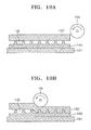
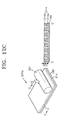
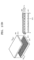
- FIGS. 10A through 10D are cross-sectional views illustrating a method of manufacturing a large-area soft mold, according to an embodiment of the present invention.
- FIG. 11 is a process flowchart illustrating a method of manufacturing a lower panel for a plasma display panel (PDP), according to an embodiment of the present invention
- FIGS. 12A through 12F are cross-sectional views illustrating the method of FIG. 11 , according to an embodiment of the present invention.
- FIG. 13 is an exploded perspective view of a PDP according to an embodiment of the present invention.
- the present invention will now be described more fully hereinafter with reference to the accompanying drawings, in which exemplary embodiments of the invention are shown.
- the present invention is largely divided into a process of manufacturing a soft mold and a process of manufacturing a barrier rib for a plasma display panel (PDP) using the soft mold.
- PDP plasma display panel
- FIG. 1 is a process flowchart illustrating a method of manufacturing a soft mold, according to an embodiment of the present invention.
- a photoresist (PR) pattern is formed on a substrate using a photolithography process in operation S101.
- a silicon mold is formed using the PR pattern as a mold and using silicon rubber as a material in operation S103.
- a metal seed layer required for an electroplating process is deposited on the silicon mold in operation S105.
- a metal mold is then manufactured by forming an electroplating layer on the silicon mold on which the metal seed layer is formed.
- the metal mold is released from the silicon mold in operation S109.
- the metal mold is imprinted on a polymer sheet to obtain a soft mold in operation S111.
- FIGS. 2A through 2D are cross-sectional views illustrating operation S101 of forming a barrier rib pattern on a base substrate 100 using a photolithography process, according to an embodiment of the present invention.
- the base substrate 100 is prepared.
- the base substrate 100 may be a glass substrate, which has a low surface roughness and a uniform surface characteristic even if it has a large area.
- a PR layer 110 is formed on the base substrate 100.
- the PR layer 110 may be obtained by coating a photosensitive resin on the base substrate 100, whereby the photosensitive resin may react with irradiated light and be cured,.
- the PR layer 110 may be a negative type dry film resist (DFR) layer.
- DFR negative type dry film resist
- a coated height "h” of the PR layer 110 corresponds to the height of a finally obtained barrier rib, the height "h” may be controlled to be in the range of about 150 to 250 ⁇ m.
- a DFR laminated layer may be prepared by stacking a plurality of DFR thin layers.
- a photo mask 120 is aligned in a predetermined position and irradiated with ultraviolet (UV) light.
- UV light may be irradiated not perpendicularly to a front surface of the photo mask 120 but at a predetermined inclination angle e to the photo mask 120.
- sides of patterns can be inclined as illustrated in FIG. 2D .
- the base substrate 100 on which the PR layer 110 is coated may be inclined to a desired angle and irradiated with UV light.
- a portion 110a which is selectively exposed by the photo mask 120, is cured due to a crosslinking reaction or a polymerization reaction, and an unexposed portion 110b which is not exposed to UV light remains uncured.
- a developing process is performed. During the developing process, the uncured portion 110b is removed to form a concave portion 111, while the cured portion 110a remains to form a convex portion 112.
- a convex portion 112 is a structure having a top surface parallel to the top surface of the underlying layer and being shorter than the bottom surface contacting the underlying layer, its cross-section thus having a trapezoidal structure.
- the side walls of the trapezoidal rib or convex portion 112 are sloped from the top of the convex portion 112 to the bottom of the convex portion 112.
- a corresponding concave portion 111 is defined by the gap between the convex portions 112.
- a PR pattern 115 which is formed by regularly alternating concave portions 111 and convex portions 112, corresponds to the finally obtained barrier rib. That is, the concave portion 111 corresponds to a discharge space in which plasma discharge occurs, and the convex portion 112 corresponds to a barrier rib that partitions the discharge spaces.
- FIG. 3 is a photographic image showing a PR barrier rib pattern obtained using the above-described process.
- the PR barrier rib pattern may be formed as a matrix type barrier rib pattern and include barrier ribs intersecting with each other.
- FIGS. 4A through 4D are cross-sectional views illustrating operation S103 of reproducing a pattern having an inverted image of the PR pattern 115 using the PR pattern 115 as a mold, according to an embodiment of the present invention.
- a shaping material 130' is coated to a large thickness on an embossed PR pattern 115 to fill the PR pattern 115.
- the shaping material 130' contains silicon rubber and a hardening agent.
- the silicon rubber may be, for example, polydimethylsiloxane (PDMS) Sylgard 184A from Dow Corning Corp.
- the silicon rubber and the hardening agent may be mixed in a ratio of 10 to 1.
- the concave portions 111 may remain unfilled.
- the shaping material 130' may be coated in a vacuum chamber for excluding inflow of air. Referring to FIG. 4C , when the PR pattern 115 is completely filled with the shaping material 130', the resultant structure is cured at a predetermined temperature and the PR pattern 115 is released as shown in FIG. 4D . Since PDMS, which is the main component of the shaping material 130', has a smooth surface and low surface energy, it has excellent release characteristics.
- FIG. 5 is a photographic of an intaglio pattern similar to that of the silicon mold 130.
- FIGS. 6A through 6C are cross-sectional views illustrating operations S105 to S109 of forming a metal mold 150 using the silicon mold 130, according to an embodiment of the present invention.
- a metal seed layer 135 is coated along the surface of the silicon mold 130. This is a preprocessing process for an electroplating process that will be performed using the metal seed layer 135 as one electrode and a plated material as the other electrode.
- Au which has high electric conductivity
- a chrome (Cr) thin layer 135b is first deposited as a under layer, and an Au thin layer 135a is formed thereon. Since the metal seed layer 135 should have enough release to separate the metal mold 150, which will be formed by electroplating, from the silicon mold 130, it must have a sufficient thickness t1. For this, the Cr thin layer 135b may be formed to a thickness of about 1000 to 5000 ⁇ , and the Au thin layer 135a may be formed to a thickness of about 1000 to 3000 ⁇ .
- the Cr thin layer 135b and the Au thin layer 135a are taken only as examples of materials required for electroplating, and the metal seed layer 135 may be formed of various known materials.
- an electroplating process is performed to form a metal plating layer 150'.
- nickel (Ni) may be used as a plated material.
- the density of the metal plating layer 150' depends on the current and voltage applied in the electroplating process.
- the metal plating layer 150' is formed to a sufficient thickness t2 to fill and cover the concave portion 131 of the silicon mold 130, the electroplating process is finished. As a result, an embossed pattern matching the silicon mold 130 is formed on a surface of the metal plating layer 150'.
- the silicon mold 130 is released to complete the metal mold 150.
- FIGS. 7A through 7D are cross-sectional views illustrating operation S111 of forming a soft mold 180 using the metal mold 150, according to an embodiment of the present invention.
- the process illustrated in FIGS. 7A through 7D is called a hot-embossing process.
- a polymer sheet 180' is disposed under the metal mold 150.
- the polymer sheet 18D' may be one of various engineering plastics, such as polycarbonate (PC), polymethyl methacrylate (PMMA), or polyethylene terephthalate (PT).
- PC polycarbonate
- PMMA polymethyl methacrylate
- PT polyethylene terephthalate
- a pattern is transferred to the polymer sheet 180'. In this case, the transfer process is performed at a high temperature in order to sufficiently shape the polymer sheet 180'.
- a specific process temperature may be optimized considering a glass transition temperature of the polymer sheet 180'.
- the metal mold 150 is imprinted onto the underlying polymer sheet 180' under high temperature conditions to form a pattern having an inverted image to the pattern of the metal mold 15D.
- an embossed pattern of the metal mold 150 is transferred to the polymer sheet 180' in intaglio.
- the resultant structure is cooled off to a normal temperature after a sufficient amount of time such that the pattern of the metal mold 150 is sufficiently transferred onto the polymer sheet 180'.
- FIG. 8A is a perspective view of the soft mold 180 manufactured using the above-described method
- FIG. 8B is a partially cutaway perspective view taken along a line A-A' of FIG. 8A , according to an embodiment of the present invention.
- the soft mold 180 includes convex portions 182 and concave portions 181, which form a predetermined pattern on a surface thereof.
- the concave portion 182 is a portion where a discharge space will be formed by performing an imprinting process on a barrier rib material.
- the concave portion 181 is a portion where a barrier rib for partitioning discharge spaces will be formed by performing the imprinting process on the barrier rib material.
- FIG. 9 is a photographic image of a soft mold formed of PET, which is obtained using the method illustrated in FIGS. 8A and 8B .
- FIGS. 7A through 7D provides an additional process of manufacturing a large-area soft mold, which will now be described with reference to FIGS. 10A through 10D .
- a metal mold 155 which is manufactured using the above-described process, is located on a base substrate 191. Thereafter, a release agent (not shown) is coated along a surface of the metal mold 155. A polymer sheet 190' is then disposed on the metal mold 155.
- the pattern of the metal mold 155 is transferred to the polymer sheet 190'.
- the transfer process is performed at a high temperature in order to sufficiently pattern the polymer sheet 190'.
- a specific process temperature may be optimized considering a glass transition temperature of the polymer sheet 190'.
- a pressure roller 195 for applying a predetermined pressure is applied to the polymer sheet 190' at least once from one end of the polymer sheet 190' to the other end thereof, so that a concave portion 156 of the metal mold 155 is gradually filled with the polymer sheet 190', thereby marking the polymer sheet 190' with a pattern of the metal mold 155.
- an embossed pattern of the metal mold 155 is transferred to the polymer sheet 190 ⁇ in intaglio.
- the pressure is applied by the pressure roller 195 until the top surface of the polymer sheet 190' is planarized, so that a uniform pattern is transferred to the entire surface of the polymer sheet 190'.
- the pressure roller 195 which rotates at uniform speed, is taken as an example of a pressure unit, the present invention is not limited thereto and any type of compressing member, which contacts the polymer sheet 190' and applies pressure thereto, may be used as the pressure unit.
- the polymer sheet 190' is released, and the metal mold 155 is removed to complete the manufacture of a large-area soft mold 190.
- the polymer sheets 190' may be supplied one by one onto the metal mold 155.
- the polymer sheets 190' may be wound as a roll around a supply roller and cut one by one before and after a pattern transferring process.
- FIG. 11 is a process flowchart illustrating a method of manufacturing a lower panel for a plasma display panel (PDP), according to an embodiment of the present invention.
- a soft mold having a top surface on which concave portions and convex portions corresponding to the shape of a barrier rib are disposed is prepared in operation S201, and a release agent (not shown) is uniformly coated along the top surface of the soft mold.
- a dielectric sheet as a material for the barrier rib is disposed on the top surface of the soft mold on which the release agent is coated.
- a barrier rib pattern formed on the soft mold is transferred onto the dielectric sheet applying pressure, e.g by using a pressure roller in operation S205.
- the dielectric sheet having the barrier rib pattern is disposed opposite a lower substrate.
- the dielectric sheet is bonded under pressure to the lower substrate, here by using the pressure roller.
- the soft mold is released.
- the barrier rib pattern formed on the dielectric sheet is sintered, thereby completing the manufacture of the lower panel.
- FIGS. 12A through 12F are cross-sectional views illustrating the method of FIG. 11 , according to an embodiment of the present invention.
- a soft mold 180 having a top surface including a plurality of concave portions 181 and a plurality of convex portions 182 corresponding to the shape of a barrier rib is prepared.
- the surface of the soft mold 180 is processed with a release agent, and a dielectric sheet 214 as a material for the barrier rib is disposed on the soft mold 180.
- a pressure roller 251 is brought into contact with the dielectric sheet 214 under a predetermined pressure and moved from one end of the dielectric sheet 214 to the other end thereof at least once at a constant rotation rate, so that a pattern of the soft mold 180 is imprinted to the dielectric sheet 214.
- the concave portions 181 of the soft mold 180 are forcibly filled with the dielectric sheet 214, and thus the dielectric sheet 214 is shaped to have a patterned layer 214a having a first thickness t1 and an unpatterned layer 214b having a second thickness t2 due to the soft mold 180.
- the shaped dielectric sheet 214 may constitute a dielectric barrier rib.
- the patterned layer 214a of the shaped dielectric sheet 214 may function as a barrier rib for partitioning discharge spaces of a PDP
- the unpatterned layer 214b of the shaped dielectric sheet 214 may function as a dielectric layer in which electrodes of the PDP are buried.
- the first thickness t1 of the patterned layer 214a is related to the dimension of the discharge spaces
- the second thickness t2 of the unpatterned layer 214b is related to the burying of the electrodes.
- FIG. 12C since pressure is applied until the top surface of the dielectric sheet 214 is planarized, a uniform pattern can be formed throughout the dielectric sheet 214.
- the dielectric sheet 214 which is patterned using the process described above, is forcibly brought into contact with a lower substrate 211 by applying pressure as will be described in more detail.
- the lower substrate 211 on which a plurality of electrodes 212 are disposed is prepared.
- the soft mold 180 and the dielectric sheet 214 which are bonded to each other under pressure, are disposed on the exposed electrodes 212 of the lower substrate 211.
- the unpatterned layer 214b of the dielectric sheet 214 is disposed opposite the exposed electrodes 212 of the lower substrate 211.
- a pressure roller 252 for applying a predetermined pressure is applied to the soft mold 180 at least once from one end of the soft mold 180 to the other end thereof at a uniform rotation rate, so that the lower substrate 211 is bonded to the dielectric sheet 214 under pressure.
- the bonding process is continued until at least the exposed electrodes 212 of the lower substrate 211 are sufficiently covered by the unpatterned layer 214b of the dielectric sheet 214 and the lower substrate 211 is reliably adhered to the dielectric sheet 214.
- the soft mold 180 is released.
- the resultant structure is sintered, thereby stabilizing the dielectric sheet 214 having a barrier rib pattern and the adhesion of the dielectric sheet 214 to the lower substrate 211.
- a barrier rib pattern can be simply manufactured by applying pressure to the soft mold using a single transfer process, as compared with a conventional method that involves a series of complicated processes, specifically, coating barrier rib paste on a substrate, forming a pattern mask for the barrier rib paste, and performing an etching process.
- the present invention provides a simple manufacturing process compared to the prior art.
- a barrier rib and a dielectric layer which are conventionally formed using separate processes, are formed in a single process according to the present invention.
- the present invention provides a dielectric barrier rib including an unpatterned layer functioning as a dielectric layer to cover electrodes and a patterned layer functioning as a barrier rib to partition discharge spaces.
- the dielectric barrier rib can be formed using a single pressure-transfer process. Therefore, the method according to the present invention can greatly reduce the number of process operations.
- the barrier rib and the lower panel for the PDP are manufactured using a soft mold, the present invention is not limited thereto and a hard mold, for example, may be used instead of the soft mold.
- FIG. 13 is an exploded perspective view of a PDP according to an embodiment of the present invention
- the PDP is largely divided into an upper panel 220 and a lower panel 210, which are bonded to each other.
- the upper panel 220 includes an upper substrate 221, a plurality of pairs of discharge sustain electrodes 226, and a dielectric layer 222 disposed on the upper substrate 221 to cover the pairs of discharge sustain electrodes 226.
- the lower panel 210 includes a lower substrate 211, a plurality of address electrodes 212 disposed on the lower substrate 211, and a barrier rib layer 214 interposed between the upper substrate 221 and the lower substrate 211 to partition a plurality of discharge spaces 230.
- the upper substrate 221 may be a display surface on which an image is projected.
- the upper substrate 221 may be a glass substrate having good optical transparency.
- the lower substrate 211 also may be a glass substrate.
- the upper and lower substrates 221 and 211 may be flexible plastic substrates having both optical transparency and flexibility.
- the pairs of discharge sustain electrodes 226 disposed under the upper substrate 221 correspond to the discharge spaces 230, respectively.
- An alternating current (AC) signal with alternating sustain pulses is applied between the pairs of discharge sustain electrodes 226 to induce sustain discharge in the corresponding discharge spaces 230.
- Discharge sustain electrodes 224 and 225 include transparent electrodes 224a and 225a, respectively, which extend across a row of discharge spaces 230, and bus electrodes 224b and 225b, respectively, which contact the transparent electrodes 224a and 225a to supply driving power.
- the present invention is not limited to the above-described electrode structure.
- the address electrodes 212 are disposed on the lower substrate 211 to cause address discharge along with the discharge sustain electrode 224 or 225.
- the address electrodes 212 may be arranged as stripes that extend at regular intervals parallel to one another and correspond to the respective discharge spaces 230.
- the barrier rib layer 214 for partitioning the respective discharge spaces 230 as independent emission regions is disposed between the upper substrate 221 and the lower substrate 211 to prevent optical and electrical crosstalk.
- the barrier rib layer 214 is obtained by imprinting a soft mold (refer to 180 in FIG. 12F ) having a barrier rib pattern to the barrier rib layer 214 (refer to 214 in FIG. 12F ).
- a patterned layer 214a having a thickness t1' which is patterned due to the soft mold
- an unpatterned layer 214b having a thickness t2' are integrally formed in the barrier rib layer 214.
- the barrier rib layer 214 constitutes a dielectric barrier rib.
- the patterned layer 214a may function as a barrier rib for partitioning the discharge spaces 230 between the upper and lower substrates 221 and 211, and the unpatterned layer 214b may function as a dielectric layer that covers the address electrodes 212.
- the unpatterned layer 214b covers and protects the underlying address electrodes 212 and functions as a conventional dielectric layer that cuts off an electrical conduction path between the address electrodes 212.
- the unpatterned layer 214b that replaces the conventional dielectric layer may be formed to a sufficient thickness t2' to prevent the occurrence of an electrical breakdown.
- the patterned layer 214a may be formed as a closed type patterned layer to enclose all sides of the discharge spaces 230 or an open type patterned layer to open some sides of the discharge spaces 230 depending on the shape of the soft mold.
- the closed-type patterned layer may be formed as a matrix type patterned layer with ribs intersecting each other to partition discharge spaces having square cross-sections.
- the closed-type patterned layer may partition polygonal discharge spaces, such as pentagonal or hexagonal discharge spaces, circular discharge spaces, or elliptical discharge spaces.
- the open-type patterned layer may be embodied by stripe patterns, but the present invention is not limited thereto.
- pattern sides 214aa that contact the discharge spaces 230 are not the etched surfaces formed using a conventional dry etching process such as a sandblasting process or a wet etching process incorporating an etchant, but the pressed surfaces formed by pressing the soft mold 180 in a downward direction.
- a conventional barrier rib that is formed by filling a liquid photosensitive paste material in a mold and curing the paste material by light is not formed using a imprinting process according the present invention
- the barrier rib formed using the liquid photosensitive paste material has sides different from the pattern sides 214aa according to the present invention.
- the pattern sides 214aa may be inclined at a predetermined angle considering the release of the barrier rib layer 214 from the soft mold 180.
- the barrier rib layer 214 is bonded under pressure to the lower substrate 211 having the address electrodes 212.
- an interface between the barrier rib layer 214 and the lower substrate 211 forms a pressure bond surface.
- a phosphor layer 215 is formed in a region corresponding to each of the discharge spaces 230.
- the phosphor layer 215 can include red (R), green (G), and blue (B) phosphor layers, which emit red, green and blue light, respectively, and are alternately coated on the pattern sides 214aa, which contact the discharge spaces 230, and bottom surfaces of the discharge spaces 230.
- the respective discharge spaces 230 form R, G, and B sub-pixels according to the type of the phosphor layer 215, and one R sub-pixel , one G sub-pixel, and one B sub-pixel form a unit pixel.
- the type of the phosphor layer 215 coated in each of the discharge spaces 230 is not restricted to R, G, and B phosphor layers, and phosphor layers 215 having different colors may be additionally included to increase the color purity of an image.
- the patterned layer 214a functions as a barrier rib that partitions the discharge spaces 230, while the unpatterned layer 214b functions as a dielectric layer.
- the barrier rib layer 214 aids in shortening the manufacturing process, but the present invention is not limited thereto.
- a dielectric layer (not shown) for covering the address electrodes 212 may be formed.
- a high-precision soft mold is provided in order to form a high-resolution barrier rib pattern.
- a precise barrier rib pattern can be formed using the soft mold.
- the present invention provides a method of manufacturing the barrier rib pattern by imprinting the soft mold to a dielectric sheet for shaping a barrier rib.
- the manufacturing process according to the present invention is simple and convenient, and a pattern of the soft mold can be accurately transferred to the dielectric sheet.
- a dielectric barrier rib which functions not only as a dielectric layer for burying electrodes but also as a barrier rib for partitioning discharge spaces, can be formed using a single imprinting process. Therefore, the number of process operations can be greatly reduced, compared with a conventional method by which a dielectric layer and a barrier rib are formed using separate processes.
- a PDP manufactured using the soft mold is provided.
- a barrier rib for partitioning respective discharge spaces as independent emission regions can be accurately formed.
- the barrier rib has improved performance, thereby enhancing the image quality of the PDP.
Landscapes
- Engineering & Computer Science (AREA)
- Chemical & Material Sciences (AREA)
- Nanotechnology (AREA)
- Manufacturing & Machinery (AREA)
- Physics & Mathematics (AREA)
- Mechanical Engineering (AREA)
- General Physics & Mathematics (AREA)
- Crystallography & Structural Chemistry (AREA)
- Mathematical Physics (AREA)
- Theoretical Computer Science (AREA)
- Condensed Matter Physics & Semiconductors (AREA)
- Gas-Filled Discharge Tubes (AREA)
Applications Claiming Priority (2)
| Application Number | Priority Date | Filing Date | Title |
|---|---|---|---|
| KR20060138904 | 2006-12-29 | ||
| KR1020070053419A KR100852121B1 (ko) | 2006-12-29 | 2007-05-31 | 격벽 형성용 소프트 몰드와, 격벽 및 하부패널의 제조방법 |
Publications (3)
| Publication Number | Publication Date |
|---|---|
| EP1938937A2 true EP1938937A2 (fr) | 2008-07-02 |
| EP1938937A3 EP1938937A3 (fr) | 2008-08-06 |
| EP1938937B1 EP1938937B1 (fr) | 2012-05-16 |
Family
ID=39313024
Family Applications (1)
| Application Number | Title | Priority Date | Filing Date |
|---|---|---|---|
| EP07124072A Not-in-force EP1938937B1 (fr) | 2006-12-29 | 2007-12-27 | Procédé de fabrication de moule souple pour mettre en forme une nervure de barrière, procédé de fabrication d'une nervure de barrière et panneau inférieur, et panneau d'affichage à plasma |
Country Status (3)
| Country | Link |
|---|---|
| US (1) | US20080157667A1 (fr) |
| EP (1) | EP1938937B1 (fr) |
| JP (1) | JP4799541B2 (fr) |
Cited By (1)
| Publication number | Priority date | Publication date | Assignee | Title |
|---|---|---|---|---|
| FR2966765A1 (fr) * | 2010-10-27 | 2012-05-04 | Modelage Concept | Procede de fabrication d'un moule et profiles permettant la realisation du moule. |
Families Citing this family (1)
| Publication number | Priority date | Publication date | Assignee | Title |
|---|---|---|---|---|
| FR3029827B1 (fr) * | 2014-12-12 | 2017-06-23 | Plastic Omnium Cie | Procede de fabrication d'une piece en matiere plastique pour vehicule automobile par ajout de matiere |
Citations (2)
| Publication number | Priority date | Publication date | Assignee | Title |
|---|---|---|---|---|
| WO2004064104A1 (fr) | 2003-01-08 | 2004-07-29 | 3M Innovative Properties Company | Moule flexible pour plaque de surface arriere de panneau d'affichage au plasma (pdp) et procedes de protection de ce moule et de cette plaque de surface arriere |
| WO2005013308A1 (fr) | 2003-07-31 | 2005-02-10 | 3M Innovative Properties Company | Modele-maitre pour reproduire une structure fine et procede de production de celui-ci |
Family Cites Families (14)
| Publication number | Priority date | Publication date | Assignee | Title |
|---|---|---|---|---|
| FR2738393B1 (fr) * | 1995-09-06 | 2000-03-24 | Kyocera Corp | Substrat d'affichage a plasma et procede pour sa fabrication |
| JP3660449B2 (ja) * | 1996-10-29 | 2005-06-15 | 鈴木総業株式会社 | 微細隔壁の形成方法 |
| WO1998057206A1 (fr) * | 1997-06-10 | 1998-12-17 | Minnesota Mining And Manufacturing Company | Connexion optique integree de type a nervure |
| JPH1142789A (ja) * | 1997-07-25 | 1999-02-16 | Murata Mfg Co Ltd | インクジェットヘッドの製造方法 |
| JP3701123B2 (ja) * | 1998-06-24 | 2005-09-28 | 株式会社日立製作所 | 隔壁転写凹版用元型の製造方法及びプラズマディスプレイパネルの隔壁形成方法 |
| US6247986B1 (en) * | 1998-12-23 | 2001-06-19 | 3M Innovative Properties Company | Method for precise molding and alignment of structures on a substrate using a stretchable mold |
| JP3204319B2 (ja) * | 1999-01-22 | 2001-09-04 | 日本電気株式会社 | ディスプレイパネルの製造方法 |
| JP2001143612A (ja) * | 1999-11-16 | 2001-05-25 | Dainippon Printing Co Ltd | 転写型および転写型の形成方法 |
| JP3601513B2 (ja) * | 2000-12-27 | 2004-12-15 | 凸版印刷株式会社 | 凹版、それを用いたプラズマディスプレイ背面板の製造方法、およびプラズマディスプレイパネル |
| JP3754337B2 (ja) * | 2001-09-28 | 2006-03-08 | 株式会社クラレ | 樹脂成形品の製造方法、樹脂成形品及び金型の製造方法 |
| JP4317375B2 (ja) * | 2003-03-20 | 2009-08-19 | 株式会社日立製作所 | ナノプリント装置、及び微細構造転写方法 |
| US20060225463A1 (en) * | 2003-07-31 | 2006-10-12 | Takaki Sugimoto | Master mold for duplicating fine structure and production method thereof |
| JP4097037B2 (ja) * | 2004-09-27 | 2008-06-04 | 株式会社日立プラズマパテントライセンシング | 隔壁転写凹版用元型の製造方法及びpdpの隔壁形成方法 |
| KR20080069074A (ko) * | 2007-01-22 | 2008-07-25 | 삼성에스디아이 주식회사 | 플라즈마 디스플레이 패널 |
-
2007
- 2007-12-27 US US11/964,993 patent/US20080157667A1/en not_active Abandoned
- 2007-12-27 JP JP2007337795A patent/JP4799541B2/ja not_active Expired - Fee Related
- 2007-12-27 EP EP07124072A patent/EP1938937B1/fr not_active Not-in-force
Patent Citations (2)
| Publication number | Priority date | Publication date | Assignee | Title |
|---|---|---|---|---|
| WO2004064104A1 (fr) | 2003-01-08 | 2004-07-29 | 3M Innovative Properties Company | Moule flexible pour plaque de surface arriere de panneau d'affichage au plasma (pdp) et procedes de protection de ce moule et de cette plaque de surface arriere |
| WO2005013308A1 (fr) | 2003-07-31 | 2005-02-10 | 3M Innovative Properties Company | Modele-maitre pour reproduire une structure fine et procede de production de celui-ci |
Cited By (1)
| Publication number | Priority date | Publication date | Assignee | Title |
|---|---|---|---|---|
| FR2966765A1 (fr) * | 2010-10-27 | 2012-05-04 | Modelage Concept | Procede de fabrication d'un moule et profiles permettant la realisation du moule. |
Also Published As
| Publication number | Publication date |
|---|---|
| JP4799541B2 (ja) | 2011-10-26 |
| JP2008166280A (ja) | 2008-07-17 |
| EP1938937A3 (fr) | 2008-08-06 |
| US20080157667A1 (en) | 2008-07-03 |
| EP1938937B1 (fr) | 2012-05-16 |
Similar Documents
| Publication | Publication Date | Title |
|---|---|---|
| JP3701123B2 (ja) | 隔壁転写凹版用元型の製造方法及びプラズマディスプレイパネルの隔壁形成方法 | |
| KR20010099913A (ko) | 신장가능한 몰드를 사용한 기판에 정밀 몰딩 및 구조체를정렬하기 위한 방법 | |
| CN101581884A (zh) | 凹版印刷板及其制造方法、电子基板和显示设备制造方法 | |
| JP2003123639A (ja) | プラズマディスプレイパネルの隔壁形成用埋め込み型ソフトモールド製造方法及びそれを利用した隔壁形成方法 | |
| EP1938937B1 (fr) | Procédé de fabrication de moule souple pour mettre en forme une nervure de barrière, procédé de fabrication d'une nervure de barrière et panneau inférieur, et panneau d'affichage à plasma | |
| CN116364815A (zh) | 量子点单元的加工方法 | |
| US6838827B2 (en) | Plasma display including certain layers being usable as high-definition large-sized display and method for fabricating the same | |
| CN101221874B (zh) | 软模具、阻挡肋和下屏板的制造方法及等离子体显示屏板 | |
| JP4097037B2 (ja) | 隔壁転写凹版用元型の製造方法及びpdpの隔壁形成方法 | |
| JP3975576B2 (ja) | 成形型 | |
| KR100813847B1 (ko) | 플라즈마 디스플레이 패널용 격벽 및 이를 포함하는 하판의제조방법 | |
| JP2002046249A (ja) | 厚膜パターン転写用凹版の元型およびその製造方法、厚膜パターン転写用凹版およびその製造方法、厚膜パターンの製造方法、プラズマディスプレイの背面基板及びその製造方法、プラズマディスプレイパネルおよびその製造方法 | |
| KR100367960B1 (ko) | 새로운 가공기술 및 조립방식을 이용한 플라즈마디스플레이 패널 하판 격벽 성형용 금형 제작 방법 | |
| JP3631594B2 (ja) | プラズマディスプレイパネルの製造方法 | |
| KR100602494B1 (ko) | 롤 성형법을 이용한 플라즈마 디스플레이 패널용 격벽제조방법 | |
| KR100730574B1 (ko) | 롤 성형법을 이용한 플라즈마 디스플레이 패널용 격벽제조방법 | |
| KR100505246B1 (ko) | 플라즈마 디스플레이 패널의 격벽 형성 방법 및 격벽 형성 장치 | |
| KR20000057223A (ko) | 비금속 분사 마스크를 이용한 분말 분사 방법 | |
| TW201241488A (en) | Color filter and method for manufacturing the same | |
| KR100366092B1 (ko) | 감광성 필름과, 이를 이용한 플라즈마 디스플레이 패널의제조방법 | |
| KR100822218B1 (ko) | 플라즈마 디스플레이 패널용 격벽 및 이를 구비한하부패널을 제조하는 방법 | |
| KR100894257B1 (ko) | 플라즈마 디스플레이 패널의 격벽 제작을 위한 유리 섬유보강 가요성 몰드 및 그 제조 방법 | |
| JPH11306965A (ja) | プラズマディスプレイパネルの隔壁形成方法 | |
| KR20000033858A (ko) | 플라즈마 어드레스 액정 표시장치의 플라즈마셀 제조방법 | |
| JPH07239410A (ja) | カラーフィルタの製造方法 |
Legal Events
| Date | Code | Title | Description |
|---|---|---|---|
| PUAI | Public reference made under article 153(3) epc to a published international application that has entered the european phase |
Free format text: ORIGINAL CODE: 0009012 |
|
| 17P | Request for examination filed |
Effective date: 20071227 |
|
| AK | Designated contracting states |
Kind code of ref document: A2 Designated state(s): AT BE BG CH CY CZ DE DK EE ES FI FR GB GR HU IE IS IT LI LT LU LV MC MT NL PL PT RO SE SI SK TR |
|
| AX | Request for extension of the european patent |
Extension state: AL BA HR MK RS |
|
| PUAL | Search report despatched |
Free format text: ORIGINAL CODE: 0009013 |
|
| AK | Designated contracting states |
Kind code of ref document: A3 Designated state(s): AT BE BG CH CY CZ DE DK EE ES FI FR GB GR HU IE IS IT LI LT LU LV MC MT NL PL PT RO SE SI SK TR |
|
| AX | Request for extension of the european patent |
Extension state: AL BA HR MK RS |
|
| AKX | Designation fees paid |
Designated state(s): DE FR GB HU |
|
| 17Q | First examination report despatched |
Effective date: 20090720 |
|
| GRAP | Despatch of communication of intention to grant a patent |
Free format text: ORIGINAL CODE: EPIDOSNIGR1 |
|
| GRAS | Grant fee paid |
Free format text: ORIGINAL CODE: EPIDOSNIGR3 |
|
| GRAA | (expected) grant |
Free format text: ORIGINAL CODE: 0009210 |
|
| AK | Designated contracting states |
Kind code of ref document: B1 Designated state(s): DE FR GB HU |
|
| REG | Reference to a national code |
Ref country code: GB Ref legal event code: FG4D |
|
| REG | Reference to a national code |
Ref country code: DE Ref legal event code: R096 Ref document number: 602007022613 Country of ref document: DE Effective date: 20120712 |
|
| PGFP | Annual fee paid to national office [announced via postgrant information from national office to epo] |
Ref country code: FR Payment date: 20121025 Year of fee payment: 6 Ref country code: DE Payment date: 20121016 Year of fee payment: 6 |
|
| PGFP | Annual fee paid to national office [announced via postgrant information from national office to epo] |
Ref country code: GB Payment date: 20121015 Year of fee payment: 6 |
|
| PLBE | No opposition filed within time limit |
Free format text: ORIGINAL CODE: 0009261 |
|
| STAA | Information on the status of an ep patent application or granted ep patent |
Free format text: STATUS: NO OPPOSITION FILED WITHIN TIME LIMIT |
|
| 26N | No opposition filed |
Effective date: 20130219 |
|
| REG | Reference to a national code |
Ref country code: DE Ref legal event code: R097 Ref document number: 602007022613 Country of ref document: DE Effective date: 20130219 |
|
| REG | Reference to a national code |
Ref country code: DE Ref legal event code: R119 Ref document number: 602007022613 Country of ref document: DE |
|
| PG25 | Lapsed in a contracting state [announced via postgrant information from national office to epo] |
Ref country code: HU Free format text: LAPSE BECAUSE OF FAILURE TO SUBMIT A TRANSLATION OF THE DESCRIPTION OR TO PAY THE FEE WITHIN THE PRESCRIBED TIME-LIMIT Effective date: 20071227 |
|
| GBPC | Gb: european patent ceased through non-payment of renewal fee |
Effective date: 20131227 |
|
| REG | Reference to a national code |
Ref country code: FR Ref legal event code: ST Effective date: 20140829 |
|
| REG | Reference to a national code |
Ref country code: DE Ref legal event code: R119 Ref document number: 602007022613 Country of ref document: DE Effective date: 20140701 |
|
| PG25 | Lapsed in a contracting state [announced via postgrant information from national office to epo] |
Ref country code: DE Free format text: LAPSE BECAUSE OF NON-PAYMENT OF DUE FEES Effective date: 20140701 |
|
| PG25 | Lapsed in a contracting state [announced via postgrant information from national office to epo] |
Ref country code: FR Free format text: LAPSE BECAUSE OF NON-PAYMENT OF DUE FEES Effective date: 20131231 Ref country code: GB Free format text: LAPSE BECAUSE OF NON-PAYMENT OF DUE FEES Effective date: 20131227 |