EP1939938A2 - Dispositif à semi-conducteur, son procédé de fabrication et conducteurs de cuivre - Google Patents
Dispositif à semi-conducteur, son procédé de fabrication et conducteurs de cuivre Download PDFInfo
- Publication number
- EP1939938A2 EP1939938A2 EP08000792A EP08000792A EP1939938A2 EP 1939938 A2 EP1939938 A2 EP 1939938A2 EP 08000792 A EP08000792 A EP 08000792A EP 08000792 A EP08000792 A EP 08000792A EP 1939938 A2 EP1939938 A2 EP 1939938A2
- Authority
- EP
- European Patent Office
- Prior art keywords
- lead
- layer
- plated
- bump
- alloy
- Prior art date
- Legal status (The legal status is an assumption and is not a legal conclusion. Google has not performed a legal analysis and makes no representation as to the accuracy of the status listed.)
- Granted
Links
Images


Classifications
-
- H—ELECTRICITY
- H10—SEMICONDUCTOR DEVICES; ELECTRIC SOLID-STATE DEVICES NOT OTHERWISE PROVIDED FOR
- H10D—INORGANIC ELECTRIC SEMICONDUCTOR DEVICES
- H10D64/00—Electrodes of devices having potential barriers
- H10D64/01—Manufacture or treatment
- H10D64/011—Manufacture or treatment of electrodes ohmically coupled to a semiconductor
-
- H—ELECTRICITY
- H10—SEMICONDUCTOR DEVICES; ELECTRIC SOLID-STATE DEVICES NOT OTHERWISE PROVIDED FOR
- H10W—GENERIC PACKAGES, INTERCONNECTIONS, CONNECTORS OR OTHER CONSTRUCTIONAL DETAILS OF DEVICES COVERED BY CLASS H10
- H10W70/00—Package substrates; Interposers; Redistribution layers [RDL]
- H10W70/40—Leadframes
- H10W70/453—Leadframes comprising flexible metallic tapes
-
- H—ELECTRICITY
- H10—SEMICONDUCTOR DEVICES; ELECTRIC SOLID-STATE DEVICES NOT OTHERWISE PROVIDED FOR
- H10W—GENERIC PACKAGES, INTERCONNECTIONS, CONNECTORS OR OTHER CONSTRUCTIONAL DETAILS OF DEVICES COVERED BY CLASS H10
- H10W70/00—Package substrates; Interposers; Redistribution layers [RDL]
- H10W70/40—Leadframes
- H10W70/456—Materials
- H10W70/457—Materials of metallic layers on leadframes
-
- H—ELECTRICITY
- H10—SEMICONDUCTOR DEVICES; ELECTRIC SOLID-STATE DEVICES NOT OTHERWISE PROVIDED FOR
- H10W—GENERIC PACKAGES, INTERCONNECTIONS, CONNECTORS OR OTHER CONSTRUCTIONAL DETAILS OF DEVICES COVERED BY CLASS H10
- H10W72/00—Interconnections or connectors in packages
- H10W72/90—Bond pads, in general
- H10W72/921—Structures or relative sizes of bond pads
- H10W72/923—Bond pads having multiple stacked layers
-
- H—ELECTRICITY
- H10—SEMICONDUCTOR DEVICES; ELECTRIC SOLID-STATE DEVICES NOT OTHERWISE PROVIDED FOR
- H10W—GENERIC PACKAGES, INTERCONNECTIONS, CONNECTORS OR OTHER CONSTRUCTIONAL DETAILS OF DEVICES COVERED BY CLASS H10
- H10W72/00—Interconnections or connectors in packages
- H10W72/90—Bond pads, in general
- H10W72/941—Dispositions of bond pads
- H10W72/9415—Dispositions of bond pads relative to the surface, e.g. recessed, protruding
Definitions
- This present invention relates to a semiconductor device provided comprising a semiconductor chip, gold (Au) bumps and copper (Cu) leads, a method of fabricating such a semiconductor device, and Cu leads. More specifically, the present invention relates to a semiconductor device that enables firm bonding of Au bumps to Cu leads, a method of fabricating such a semiconductor device, and Cu leads.
- the semiconductor chip of a conventional semiconductor device to be connected to leads by a tape-automated bonding method generally is provided with bumps, i.e., metal electrodes, on electrode pads.
- a conventional semiconductor device 1 has a semiconductor chip 1a provided with electrode pads 2.
- electrode pads 2 In Fig. 20 , only one of the electrode pads 2 is shown.
- the surface of the semiconductor chip 1a on which the electrode pads 2 are formed is coated entirely with a passivation film 3 of Si 3 N 4 or SiO 2 , and the surfaces of the electrode pads 2 are exposed partially through openings 4 formed in the passivation film 3, respectively.
- a barrier metal layer 5 is formed so as to cover the exposed portion of each electrode pad 2, and an area of the passivation film 3 around the edge of the opening 4.
- the barrier metal layer 5 consists of a plurality of metal thin films.
- the barrier metal layer 5 shown in Fig. 20 by way of example is formed by sequentially forming a first barrier metal layer 5a of titanium (Ti), a second barrier metal layer 5b of nickel (Ni) and a third barrier metal layer 5c of palladium (Pd).
- a bump 6 is formed on the third barrier metal layer 5c.
- the bumps 6 of semiconductor devices to be mounted on a TAB tape by a TAB method are formed of Au.
- an inner lead 7 i.e., a portion of a Cu lead of a TAB tape, is bonded to the bump 6 by a bonding process, i.e., an inner lead bonding process (ILB process).
- the Cu leads are coated with a 0.4 to 0.6 ⁇ m thick plated tin (Sn) layer.
- the Cu lead coated with the plated Sn layer has an inner lead 7 and an outer lead.
- the thickness of a portion of the plated Sn layer on the side of the outer lead of the Cu lead must be sufficiently large for reliable outer lead bonding; otherwise Cu appears on the surface of the outer lead, which will lead to entailing problems in oxidation of Cu and then less wettability during bonding. Therefore, the thickness of the plated Sn layer coating the outer lead of the Cu lead must be in the range of 0.4 to 0.6 ⁇ m, and hence, generally, the thickness of the plated Sn layer on the inner leads is in the range of 0.4 to 0.6 ⁇ m as mentioned above.
- the inner lead 7 When bonding together the inner lead 7 and the Au bump 6 by inner lead bonding (ILB), the the inner lead 7 is brought into contact with the Au bump 6, and then heat and pressure are applied to the interface between the inner lead 7 and the Au bump 6.
- ILB inner lead bonding
- the inner lead 7 and the Au bump 6 are thus bonded together, fillets 8 are formed on the side surfaces of the inner lead 7, and an alloy layer 9 is formed in the interface between the inner lead 7 and the Au bump 6.
- the fillet 8 and the alloy layer 9 secure the bonding strength between the inner lead 7 and the Au bump 6.
- the fillet 8 and the alloy layer 9 formed when the Au bump 6 and the inner lead 7 coated with the plated Sn layer are bonded together are formed of An Au-Sn alloy;
- the fillet 8 is formed mainly of a eutectic Au-Sn alloy (70.7 at.% Au and 29.3 at.% Sn ( M. Hansen, "Contribution of Binary Alloys", Genium Publishing Corp., New York (1985 )), and the alloy layer 9 is formed of a eutectic Au-Sn alloy or a zeta-phase Au-Sn alloy (84 to 88 at.% Au and 12 to 16 at.% Sn) ( Bike Zakel, et al., 42nd ECTC Proceeding, pp.
- the alloy layer 9 is formed of such an Au-Sn alloy because the plated Sn layer coating the inner lead 7 has a comparatively large thickness of 0.4 to 0.6 ⁇ m and and hence it is difficult for Cu forming the inner lead 7 to appear on the surface of the plated Sn layer.
- a high-temperature stability test is a representative accelerated durability tests.
- the high-temperature stability test uses a property of metals that the diffusion rate of metals at a high temperature is higher than that at an ordinary temperature.
- Cu forming the inner lead 7 diffuses into the fillets 8 formed on the side surfaces of the inner lead, forming voids (defects) in the Cu inner lead 7 by the Kirkendall effect.
- Cu forming the inner lead 7 diffuses into the alloy layer 9, causing the alloy layer 9 originally being of an Au-Sn alloy of a binary alloy system to change into an Au-Cu-Sn alloy of a ternary alloy system.
- the alloy layer 9 changes into such an alloy of a ternary alloy system, voids are formed in the surface of the inner lead 7 on the side of the semiconductor chip 1a due to the Kirkendall effect. If the voids grows, it is possible that the inner lead 7 is disconnected from the Au bump 6.
- Zakel, et al. made a detailed report on the condition of bonding parts formed by ILB after the bonding parts had been kept in a high-temperature environment in Elke Zakel, et al., 42nd ECTC Proceeding, pp. 360-371 (1992 ).
- the plated Sn layer coating the inner lead 7 of a TAB tape was formed in a thickness of 0.7 ⁇ m by an electroplating process, the heating temperature for ILB was 400 to 500°C and the ILB pressure applied to the bumps was 10 or 40 cN (10 or 40 gf).
- the ILB pressure is comparatively low, a eutectic Au-Sn alloy is formed in the alloy layer 9.
- Cu of the inner leads 7 diffuses into eutectic Au-Sn portions of the alloy layer 9, and voids are formed by the Kirkendall effect when the Au-Sn alloy changes into an Au-Cu-Sn alloy.
- a zeta phase is formed mainly in the alloy layer 9 and Cu of the inner lead 7 does not diffuse into the alloy layer 9 during the high-temperature stability test when the ILB pressure is comparatively high, which is inferred to be due the extrusion of the eutectic Au-Sn alloy formed during ILB from the bonding part by the comparatively high ILB pressure and the resultant formation of a zeta phase in which the Sn content is comparatively small.
- Zakel, et al. concluded that the zeta phase thus formed serves as a barrier against the diffusion of Cu to suppress the formation of voids and, consequently, the reliability of the bonding part is enhanced.
- an Au-Sn alloy having a high Sn content remains locally in the bonding part and voids are possible to grow from portions of the bonding part having a high Sn content.
- the present invention has been made in view of such problems and it is therefore an object of the present invention to provide a semiconductor device that enables firm bonding of Au bumps to Cu leads, a method of fabricating such a semiconductor device and a copper lead.
- a semiconductor device in a first aspect of the present invention comprises a semiconductor chip, an Au bump formed on the semiconductor chip, and a Cu lead bonded by a bonding part to the Au bump, in which the Cu lead has a Cu core and a plated Sn layer formed on the Cu core, and the bonding part is formed of an Au-Cu-Sn alloy of a ternary system.
- a semiconductor device in a second aspect of the present invention comprises a semiconductor chip, an Au bump formed on the semiconductor chip, and a Cu lead bonded by a bonding part to the Au bump, in which the Cu lead comprises a Cu core and a plated Sn layer formed on the Cu core, and an Au-Cu alloy of a binary alloy system is formed in the bonding part.
- a Cu lead in a third aspect of the present invention comprises a Cu core and a plated Sn layer formed on the Cu core, and has an inner lead and an outer lead, in which the thickness of the plated Sn layer of the inner lead is in the range of 0.15 to 0.35 ⁇ m.
- a method of fabricating a semiconductor device in a fourth aspect of the present invention comprises the steps of: preparing a semiconductor chip provided with an Au bump, and bonding a Cu lead having a Cu core and a plated Sn layer formed on the Cu core to the Au bump; so that a bonding part of an Au-Cu-Sn alloy having an Au-rich single-phase structure including 15 at.% or less Sn and 25 at.% or less Cu is formed between the Au bump and the corresponding Cu lead.
- a method of fabricating a semiconductor device in a fifth aspect of the present invention comprises the steps of: preparing a semiconductor chip provided with an Au bump, bonding Cu lead comprising a Cu core and a plated Sn layer formed on the Cu core to the Au bumps, and keeping the Au bump and the Cu lead at a predetermined temperature for a given time, so that a bonding part of an Au-Cu alloy of a substantially binary alloy system is formed between the Au bump and the corresponding Cu lead.
- Sn of the Au-Cu-Sn alloy of a ternary alloy system forming the bonding part between the Au bump and the Cu leads can be expelled from the bonding part when the semiconductor device is used for a long time in a working environment of an ordinary temperature or in a working environment of a high temperature to form an Au-Cu alloy of a binary alloy system in the bonding part.
- an Au-Cu-Sn alloy of a ternary alloy system can be formed in the bonding part when the Cu lead is bonded to the Au bump, because the thickness of the plated Sn layer of the inner lead is in the range of 0.15 to 0.35 ⁇ m.
- a firm, stable bonding part of an Au-rich Au-Cu-Sn alloy having a single-phase structure containing 15 at.% or less Sn and 25 at.% or less Cu can be formed between the Au bump and the Cu lead.
- a firm, stable bonding part of an Au-Cu alloy of a binary alloy system can be formed between the Au bump and the Cu lead.
- a semiconductor device in a preferred embodiment according to the present invention will be generally described with reference to Figs. 15 and 16 .
- a semiconductor device 1 in accordance with the present invention comprises a semiconductor chip la, Au bumps 6 formed on the semiconductor chip la, and Cu leads 12 bonded to the Au bumps 6, respectively.
- Each Cu lead 12 has an inner lead 7 bonded to the Au bump 6, and an outer lead 11 connected to the inner lead 7.
- the Cu leads 12 are arranged beforehand on a resin film 16.
- the Cu leads 12 and the resin film 16 constitute a TAB tape 15.
- the resin film 16 of the TAB tape 15 is provided with outer lead holes 17 across which the outer leads 11 extend, a device hole 18 in which the semiconductor chip 1a is disposed, and tooling holes 19 for tape feeding and positioning. After the semiconductor chip 1a has been connected to the TAB tape 15, the TAB tape 15 is cut along the outer lead holes 17 to separate the semiconductor device 1 from the TAB tape 15, and the semiconductor device 1 is mounted on a printed wiring board, not shown.
- the semiconductor chip 1a of the semiconductor device 1 is provided with electrode pads 2 of aluminum, and the surface of the semiconductor device 1 on which the electrode pads 2 are formed is coated entirely with a passivation film 3 of SiN 4 or SiO 2 .
- the passivation film 3 is provided with openings 4 at positions corresponding to the electrode pads 2 to expose the electrode pads 2 partially through the openings 4.
- a barrier metal layer 5 is formed so as to cover the exposed surface of each electrode pad 2 and an area of the passivation film 3 around the edge of the opening 4.
- the barrier metal layer 5 consists of a plurality of metal thin films.
- the barrier metal layer 5 shown in Fig. 1 is formed by sequentially forming a first barrier metal layer 5a of Ti, a second barrier metal layer 5b of Ni and a third barrier metal layer 5c of Pd.
- the bump 6 is formed on the third barrier metal layer 5c.
- the bumps 6 of semiconductor devices to be mounted on a TAB tape by a TAB method are formed of Au.
- the inner lead 7 of the Cu lead 12 is bonded to the Au bump 6 by an ILB process.
- the Cu lead 12 consists of a Cu core 12a and a plated Sn layer 12b formed on (coating) the Cu core 12a.
- the plated Sn layer 12b is formed by an electroless plating process.
- the thickness of a first portion of the plated Sn layer 12b coating the Cu core 12a of the inner lead 7 and that of a second portion of the same coating the Cu core 12a of the outer lead 11 are different from each other; the respective thicknesses of the first and the second portion of the plated Sn layer 12b measured by a coulometric thickness meter are in the range of 0.15 to 0.35 ⁇ m and in the range of 0.4 to 0.6 ⁇ m, respectively.
- the second portion of the plated Sn layer 12b coating the Cu core 12a of the outer lead 11 has a comparatively large thickness in the range of 0.4 to 0.6 ⁇ m, Cu will not appear on the surface of the outer lead 11 during outer lead bonding (OLB), as a result of that the Cu core 12a will not be oxidized and therefore moderate wettability can be secured.
- the thickness of the plated Sn layer 12b of the outer lead 11 may be less than 0.4 ⁇ m.
- the plated Sn layer 12b is subjected to heat treatment immediately after being formed on the surface of the Cu core 12a to make Sn of the plated Sn layer 12b diffuse into the Cu core 12a.
- Fig. 2 is a graph showing the variation of Sn content of the Cu leads 12 having plated Sn layers 12b of different thicknesses of 0.1 to 0.4 ⁇ m respectively, with depth from the surface measured immediately after heat-processing the Cu leads 12 after forming the plated Sn layers 12b by Rutherford backscattering spectroscopy.
- the Sn content of the surface of each plated Sn layer 12b of a thickness of 0.4 ⁇ m or below is less than 100 at.%, which proves that Cu is present in the surface of the plated Sn layer 12b.
- the thickness of the first portion of the plated Sn layer 12b coating the Cu core 12a of the inner lead 7 is in the range of 0.15 to 0.35 ⁇ m and, in the first portion of the plated Sn layer 12b, the ratio of Cu to Sn in atomic percent on the surface of the plated Sn layer 12b is 5 : 95 to 25 : 75 ( Fig. 2 ).
- the thickness of the second portion of the plated Sn layer 12b coating the Cu core 12a of the outer lead 11 is in the range of 0.4 to 0.6 ⁇ m and, in the second portion of the plated Sn layer 12b, the ratio of Cu to Sn in atomic percent on the surface of the plated Sn layer 12b is 0 : 100 to 5 : 95 ( Fig. 2 ).
- the electrode pads 2 are formed on the semiconductor chip 1a.
- the barrier metal layers 5 and the Au bumps 6 are formed in that order on the electrode pads 2, respectively.
- the inner leads 7 of the Cu leads 12 each formed by coating the Cu core 12a with the plated Sn layer 12b are brought into contact with the Au bumps 6, respectively, and heat and pressure are applied to the inner leads 7 for ILB to bond the inner leads 7 to the Au bumps 6, respectively.
- fillets 8 are formed on the side surfaces of each inner lead 7, and an alloy layer (bonding part) 10 is formed in the interface between the inner lead 7 and the Au bump 6.
- the fillets 8 and the alloy layer 10 secure bonding strength between the inner lead 7 and the Au bump 6.
- Fig. 3 is a photograph of a section of the bonding part 10 between the Au bump 6 and the inner lead 7 taken by scanning electron microscopy (SEM), and Figs. 4 , 5 and 6 are photographs showing the respective distributions of Au, Cu and Sn, respectively, in the alloy layer 10 between the Au bump 6 and the inner lead 7.
- numerals indicate contents in percent by weight, darker areas correspond to regions having a higher content, and lighter areas correspond to regions having a lower content.
- a temperature of 500°C and a pressure of 70 MPa are conditions for the ILB of the inner lead 7 to the Au bump 6.
- the thickness of the plated Sn layer 12b of the inner lead 7 is 0.28 ⁇ m.
- the Au/Sn ratio of the composition of the fillet 8 is nearly equal to that of an eutectic alloy, and the alloy layer 10 is an Au-Cu-Sn alloy of a ternary system.
- the alloy layer 10 of an Au-Cu-Sn alloy of a ternary system is formed when the inner lead 7 is bonded to the Au bump 6 by ILB because the plated Sn layer 12b of the inner lead 7 has a comparative small thickness in the range of 0.15 to 0.35 ⁇ m and hence Cu appears from the Cu lead core 12a to the surface of the plated Sn layer 12b in a Cu content of 5 to 25% at..
- the composition Au : Cu : Sn in atomic percent of the alloy forming the alloy layer 10 is 61.9 : 24.2 : 14.1 and the alloy of the alloy layer 10 is not a eutectic alloy but is an Au-rich simple alloy. Experiments showed that such an Au-rich simple alloy can be obtained when the Cu content is 25% at. or below and the Sn content is 15 at.% or below. Since Sn is comparatively unstable in an Au-rich alloy, Sn is expelled from the alloy layer 10 when the semiconductor device 1 is kept at a high temperature or at an ordinary temperature for a long time.
- Fig. 7 is a photograph showing a section of the alloy layer 10 and its vicinity shown in Figs. 3 to 6 in the semiconductor device 1 after the semiconductor device 1 has been kept at 200°C for for 240 h
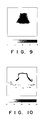
- Figs. 8 , 9 and 10 are photographs showing the distributions of Au, Cu and Sn in the bonding part 10 between the Au bump 6 and the inner lead 7 after the semiconductor device 1 has been kept at 200°C for 240 h.
- figures indicate content in percent by weight, darker areas correspond to regions having a higher content, and lighter areas correspond to regions having a lower content. As is evident from Figs.
- the Au-Cu alloy forming the alloy layer 10 may contain Sn in a small Sn content of, for example, 5 at.% or below.
- Sn in a small Sn content of, for example, 5 at.% or below.
- an Au-Cu-Sn alloy of a ternary system having a high bonding strength can be formed in the alloy layer 10 during the ILB of the inner lead 7 to the Au bump 6 when the ILB pressure is 50 MPa or above.
- the thickness of the plated Sn layers 12b of sample inner leads subjected to experiments for obtaining the results shown in Fig. 17 is 0.25 ⁇ m and the ILB temperature for forming sample alloy layers for obtaining the results shown in Fig. 17 is 500°C. If the thickness of the plated Sn layer 12b is 0.15 ⁇ m or below, the Cu content on the surface of the inner lead 7 is excessively high and any satisfactory alloy cannot be formed by ILB. If the thickness of the plated Sn layer 12b measured by a coulometric thickness meter is greater than 0.35 ⁇ m, Cu is hardly able to appear to the surface of the inner lead 7 and, consequently, an alloy of a ternary system cannot be formed.
- the depth of diffusion of Sn from the surface of the plated Sn layer 12b in the inner lead 7 is greater than 1.2 ⁇ m, surplus Sn collects at the lead neck during ILB and may possibly cause accidental connection between the adjacent inner leads 7. Therefore, the depth of diffusion of Sn is, desirably, 1.2 ⁇ m or below.
- Fig. 18 showing the dependence of the bonding strength of the alloy layer 10 on ILB temperature, it is difficult to form a satisfactory alloy layer 10 when the ILB temperature is lower than 450°C.
- the thickness of the plated Sn layers 12b of sample inner leads subjected to experiments for obtaining the results shown in Fig. 18 is 0.25 ⁇ m and the ILB pressure for forming sample alloy layers for obtaining the results shown in Fig. 17 is 70 MPa.
- the bonding strength of the alloy layer 10 decreases when the ILB temperature increased beyond 550°C, which is inferred to be due to the excessive formation of an alloy at the neck of the inner lead 7. Therefore, the ILB temperature must be in the range of 450°C to 550°C.
- Figs. 11 to 14 Changes that occur when the semiconductor device 1 is kept at 200°C for 720 h will be described with reference to Figs. 11 to 14 .
- Conditions for the ILB of an inner lead having a 0.28 ⁇ m thick plated Sn layer to an Au bump are 500°C in ILB temperature and 70 MPa in ILB pressure.
- Fig. 11 is a photograph showing the metallographic structure of a bonding part after the bonding part has been kept at 200°C for 720 h and
- Figs. 12 , 13 and 14 are photographs showing the distribution of Au, Cu and Sn in an alloy layer 10 shown in Fig. 11 .
- Figs. 11 is a photograph showing the metallographic structure of a bonding part after the bonding part has been kept at 200°C for 720 h
- Figs. 12 , 13 and 14 are photographs showing the distribution of Au, Cu and Sn in an alloy layer 10 shown in Fig. 11 .
- Figs. 11 is a photograph showing
- activation energy which must be added to the alloy layer 10 to allow a reaction through which the Au-Cu-Sn alloy changes into an Au-Cu alloy of a binary system is 0.37 eV mentioned in the paper of Zakel, et al. as activation energy necessary for activating an Au-Cu-Sn alloy.
- an Au-Cu alloy of a binary system is formed in the bonding area in about five years if the ambient temperature is 25°C and the temperature of the alloy layer 10 is 50 ° C while the semiconductor device 1 is in operation or in about one year if the ambient temperature is 25°C and the temperature of the alloy layer 10 is 100°C while the semiconductor device 1 is in operation.
Landscapes
- Wire Bonding (AREA)
- Lead Frames For Integrated Circuits (AREA)
- Internal Circuitry In Semiconductor Integrated Circuit Devices (AREA)
Applications Claiming Priority (3)
| Application Number | Priority Date | Filing Date | Title |
|---|---|---|---|
| JP3595995 | 1995-02-01 | ||
| JP34640595A JP3296400B2 (ja) | 1995-02-01 | 1995-12-12 | 半導体装置、その製造方法およびCu製リード |
| EP96101412A EP0725437B1 (fr) | 1995-02-01 | 1996-02-01 | Dispositif semi-conducteur et méthode de fabrication associé |
Related Parent Applications (1)
| Application Number | Title | Priority Date | Filing Date |
|---|---|---|---|
| EP96101412A Division EP0725437B1 (fr) | 1995-02-01 | 1996-02-01 | Dispositif semi-conducteur et méthode de fabrication associé |
Publications (3)
| Publication Number | Publication Date |
|---|---|
| EP1939938A2 true EP1939938A2 (fr) | 2008-07-02 |
| EP1939938A3 EP1939938A3 (fr) | 2008-07-09 |
| EP1939938B1 EP1939938B1 (fr) | 2014-07-23 |
Family
ID=26374978
Family Applications (2)
| Application Number | Title | Priority Date | Filing Date |
|---|---|---|---|
| EP96101412A Expired - Lifetime EP0725437B1 (fr) | 1995-02-01 | 1996-02-01 | Dispositif semi-conducteur et méthode de fabrication associé |
| EP08000792.5A Expired - Lifetime EP1939938B1 (fr) | 1995-02-01 | 1996-02-01 | Dispositif à semi-conducteur, son procédé de fabrication et conducteurs de cuivre |
Family Applications Before (1)
| Application Number | Title | Priority Date | Filing Date |
|---|---|---|---|
| EP96101412A Expired - Lifetime EP0725437B1 (fr) | 1995-02-01 | 1996-02-01 | Dispositif semi-conducteur et méthode de fabrication associé |
Country Status (6)
| Country | Link |
|---|---|
| US (2) | US5747881A (fr) |
| EP (2) | EP0725437B1 (fr) |
| JP (1) | JP3296400B2 (fr) |
| KR (1) | KR100237940B1 (fr) |
| DE (1) | DE69637728D1 (fr) |
| TW (1) | TW299490B (fr) |
Families Citing this family (37)
| Publication number | Priority date | Publication date | Assignee | Title |
|---|---|---|---|---|
| DE19524739A1 (de) * | 1994-11-17 | 1996-05-23 | Fraunhofer Ges Forschung | Kernmetall-Lothöcker für die Flip-Chip-Technik |
| JP3296400B2 (ja) * | 1995-02-01 | 2002-06-24 | 東芝マイクロエレクトロニクス株式会社 | 半導体装置、その製造方法およびCu製リード |
| US6075289A (en) * | 1996-10-24 | 2000-06-13 | Tessera, Inc. | Thermally enhanced packaged semiconductor assemblies |
| JP3030271B2 (ja) * | 1997-05-19 | 2000-04-10 | 富士通株式会社 | 半導体部品の実装方法 |
| DE19730118B4 (de) | 1997-07-14 | 2006-01-12 | Infineon Technologies Ag | Verfahren und Vorrichtung zur Herstellung einer Chip-Substrat-Verbindung |
| CN1151547C (zh) * | 1997-07-15 | 2004-05-26 | 株式会社日立制作所 | 半导体装置制造方法 |
| JPH11243208A (ja) * | 1998-02-26 | 1999-09-07 | Mitsubishi Electric Corp | 半導体装置及びその製造方法 |
| MY139405A (en) * | 1998-09-28 | 2009-09-30 | Ibiden Co Ltd | Printed circuit board and method for its production |
| US6359328B1 (en) * | 1998-12-31 | 2002-03-19 | Intel Corporation | Methods for making interconnects and diffusion barriers in integrated circuits |
| JP3287328B2 (ja) | 1999-03-09 | 2002-06-04 | 日本電気株式会社 | 半導体装置及び半導体装置の製造方法 |
| US6249044B1 (en) * | 1999-06-17 | 2001-06-19 | National Semiconductor Corp. | Opaque metallization to cover flip chip die surface for light sensitive semiconductor devices |
| EP1139413B1 (fr) * | 2000-03-24 | 2005-03-16 | Texas Instruments Incorporated | Procédé de microcablage |
| JP4387548B2 (ja) | 2000-03-28 | 2009-12-16 | 株式会社東芝 | 半導体装置及びその製造方法 |
| JP3459223B2 (ja) * | 2000-04-19 | 2003-10-20 | 沖電気工業株式会社 | 半導体装置及びその製造方法 |
| US6462426B1 (en) * | 2000-12-14 | 2002-10-08 | National Semiconductor Corporation | Barrier pad for wafer level chip scale packages |
| US6426556B1 (en) * | 2001-01-16 | 2002-07-30 | Megic Corporation | Reliable metal bumps on top of I/O pads with test probe marks |
| US6445069B1 (en) * | 2001-01-22 | 2002-09-03 | Flip Chip Technologies, L.L.C. | Electroless Ni/Pd/Au metallization structure for copper interconnect substrate and method therefor |
| US6815324B2 (en) | 2001-02-15 | 2004-11-09 | Megic Corporation | Reliable metal bumps on top of I/O pads after removal of test probe marks |
| TWI245402B (en) * | 2002-01-07 | 2005-12-11 | Megic Corp | Rod soldering structure and manufacturing process thereof |
| TWI281718B (en) * | 2002-09-10 | 2007-05-21 | Advanced Semiconductor Eng | Bump and process thereof |
| US6784089B2 (en) * | 2003-01-13 | 2004-08-31 | Aptos Corporation | Flat-top bumping structure and preparation method |
| JP2004281491A (ja) * | 2003-03-13 | 2004-10-07 | Toshiba Corp | 半導体装置及びその製造方法 |
| US7335536B2 (en) * | 2005-09-01 | 2008-02-26 | Texas Instruments Incorporated | Method for fabricating low resistance, low inductance interconnections in high current semiconductor devices |
| US9524945B2 (en) | 2010-05-18 | 2016-12-20 | Taiwan Semiconductor Manufacturing Company, Ltd. | Cu pillar bump with L-shaped non-metal sidewall protection structure |
| US8841766B2 (en) | 2009-07-30 | 2014-09-23 | Taiwan Semiconductor Manufacturing Company, Ltd. | Cu pillar bump with non-metal sidewall protection structure |
| US8377816B2 (en) * | 2009-07-30 | 2013-02-19 | Taiwan Semiconductor Manufacturing Company, Ltd. | Method of forming electrical connections |
| US8324738B2 (en) | 2009-09-01 | 2012-12-04 | Taiwan Semiconductor Manufacturing Company, Ltd. | Self-aligned protection layer for copper post structure |
| US8659155B2 (en) | 2009-11-05 | 2014-02-25 | Taiwan Semiconductor Manufacturing Company, Ltd. | Mechanisms for forming copper pillar bumps |
| US8610270B2 (en) | 2010-02-09 | 2013-12-17 | Taiwan Semiconductor Manufacturing Company, Ltd. | Semiconductor device and semiconductor assembly with lead-free solder |
| US8441124B2 (en) * | 2010-04-29 | 2013-05-14 | Taiwan Semiconductor Manufacturing Company, Ltd. | Cu pillar bump with non-metal sidewall protection structure |
| US9018758B2 (en) | 2010-06-02 | 2015-04-28 | Taiwan Semiconductor Manufacturing Company, Ltd. | Cu pillar bump with non-metal sidewall spacer and metal top cap |
| US8546254B2 (en) | 2010-08-19 | 2013-10-01 | Taiwan Semiconductor Manufacturing Company, Ltd. | Mechanisms for forming copper pillar bumps using patterned anodes |
| US8437142B2 (en) * | 2011-06-20 | 2013-05-07 | Chipbond Technology Corporation | Bump structure and process of manufacturing the same |
| US20150262952A1 (en) * | 2014-03-13 | 2015-09-17 | Taiwan Semiconductor Manufacturing Co., Ltd | Bump structure and method for forming the same |
| US10107662B2 (en) * | 2015-01-30 | 2018-10-23 | Honeywell International Inc. | Sensor assembly |
| KR102534735B1 (ko) | 2016-09-29 | 2023-05-19 | 삼성전자 주식회사 | 필름형 반도체 패키지 및 그 제조 방법 |
| CN111257995A (zh) * | 2020-02-12 | 2020-06-09 | 深圳技术大学 | 一种高折射率差yag单晶异质结构薄膜波导及其制备方法 |
Family Cites Families (4)
| Publication number | Priority date | Publication date | Assignee | Title |
|---|---|---|---|---|
| US4634638A (en) * | 1981-12-17 | 1987-01-06 | International Business Machines Corporation | High melting point copper-gold-tin brazing alloy for chip carriers |
| JPH06151616A (ja) * | 1992-11-14 | 1994-05-31 | Toshiba Corp | 半導体集積回路装置及びその製造方法 |
| US5545589A (en) * | 1993-01-28 | 1996-08-13 | Matsushita Electric Industrial Co., Ltd. | Method of forming a bump having a rugged side, a semiconductor device having the bump, and a method of mounting a semiconductor unit and a semiconductor device |
| JP3296400B2 (ja) * | 1995-02-01 | 2002-06-24 | 東芝マイクロエレクトロニクス株式会社 | 半導体装置、その製造方法およびCu製リード |
-
1995
- 1995-12-12 JP JP34640595A patent/JP3296400B2/ja not_active Expired - Fee Related
-
1996
- 1996-01-24 TW TW085100824A patent/TW299490B/zh not_active IP Right Cessation
- 1996-01-30 US US08/593,622 patent/US5747881A/en not_active Expired - Lifetime
- 1996-02-01 KR KR1019960002412A patent/KR100237940B1/ko not_active Expired - Fee Related
- 1996-02-01 EP EP96101412A patent/EP0725437B1/fr not_active Expired - Lifetime
- 1996-02-01 DE DE69637728T patent/DE69637728D1/de not_active Expired - Lifetime
- 1996-02-01 EP EP08000792.5A patent/EP1939938B1/fr not_active Expired - Lifetime
-
1997
- 1997-05-09 US US08/853,475 patent/US6049130A/en not_active Expired - Lifetime
Non-Patent Citations (2)
| Title |
|---|
| BIKE ZAKEL ET AL., 42ND ECTC PROCEEDING, 1992, pages 360 - 371 |
| ELKE ZAKEL ET AL., 42ND ECTC PROCEEDING, 1992, pages 360 - 371 |
Also Published As
| Publication number | Publication date |
|---|---|
| JP3296400B2 (ja) | 2002-06-24 |
| EP0725437B1 (fr) | 2008-10-29 |
| JPH08274129A (ja) | 1996-10-18 |
| US6049130A (en) | 2000-04-11 |
| EP0725437A2 (fr) | 1996-08-07 |
| EP1939938A3 (fr) | 2008-07-09 |
| DE69637728D1 (de) | 2008-12-11 |
| TW299490B (fr) | 1997-03-01 |
| KR960032613A (ko) | 1996-09-17 |
| EP1939938B1 (fr) | 2014-07-23 |
| US5747881A (en) | 1998-05-05 |
| KR100237940B1 (ko) | 2000-01-15 |
| EP0725437A3 (fr) | 1998-11-18 |
Similar Documents
| Publication | Publication Date | Title |
|---|---|---|
| EP1939938B1 (fr) | Dispositif à semi-conducteur, son procédé de fabrication et conducteurs de cuivre | |
| KR100482721B1 (ko) | 배선 기판 및 그 제조 방법, 반도체 장치 및 그 제조방법, 및 전자 기기 | |
| US6294828B1 (en) | Semiconductor chip package | |
| US5134460A (en) | Aluminum bump, reworkable bump, and titanium nitride structure for tab bonding | |
| US4463059A (en) | Layered metal film structures for LSI chip carriers adapted for solder bonding and wire bonding | |
| JP2543619B2 (ja) | 半導体装置用リ―ドフレ―ム | |
| US5684329A (en) | Lead frame for semiconductor device | |
| US6452271B2 (en) | Interconnect component for a semiconductor die including a ruthenium layer and a method for its fabrication | |
| US5801436A (en) | Lead frame for semiconductor device and process for producing the same | |
| US4513905A (en) | Integrated circuit metallization technique | |
| US3982908A (en) | Nickel-gold-cobalt contact for silicon devices | |
| US7018721B2 (en) | Structure for interconnecting conductors and connecting method | |
| US7408248B2 (en) | Lead frame for semiconductor device | |
| EP0256357B1 (fr) | Puce semi-conductrice comprenant une structure à protubérance pour le transport automatique sur bande | |
| US4065588A (en) | Method of making gold-cobalt contact for silicon devices | |
| JPS5936426B2 (ja) | Ic用リ−ドフレ−ム | |
| JPH1074879A (ja) | 半導体装置用リードフレーム | |
| US5563449A (en) | Interconnect structures using group VIII metals | |
| JP2858197B2 (ja) | 半導体装置用リードフレーム | |
| JP3265814B2 (ja) | バンプ電極を有する回路基板 | |
| KR101167650B1 (ko) | 반도체 장치용 리드 프레임 | |
| JP3466498B2 (ja) | 配線基板及びその製造方法 | |
| JPS6244817B2 (fr) | ||
| JPH11186483A (ja) | 半導体装置用リードフレーム | |
| JPH06140544A (ja) | 半導体装置 |
Legal Events
| Date | Code | Title | Description |
|---|---|---|---|
| PUAI | Public reference made under article 153(3) epc to a published international application that has entered the european phase |
Free format text: ORIGINAL CODE: 0009012 |
|
| PUAL | Search report despatched |
Free format text: ORIGINAL CODE: 0009013 |
|
| 17P | Request for examination filed |
Effective date: 20080116 |
|
| AC | Divisional application: reference to earlier application |
Ref document number: 0725437 Country of ref document: EP Kind code of ref document: P |
|
| AK | Designated contracting states |
Kind code of ref document: A2 Designated state(s): DE FR GB |
|
| AK | Designated contracting states |
Kind code of ref document: A3 Designated state(s): DE FR GB |
|
| RIN1 | Information on inventor provided before grant (corrected) |
Inventor name: SHIBAZAKI, KOJI,C/O INTELLECTUAL PROPERTY DIVISION Inventor name: TAZAWA, HIROSHI,C/O INTELLECTUAL PROPERTY DIVISION Inventor name: HOSOMI, EIICHI Inventor name: TAKUBO, CHIAKI,C/O INTELLECTUAL PROPERTY DIVISION |
|
| 17Q | First examination report despatched |
Effective date: 20081006 |
|
| AKX | Designation fees paid |
Designated state(s): DE FR GB |
|
| GRAP | Despatch of communication of intention to grant a patent |
Free format text: ORIGINAL CODE: EPIDOSNIGR1 |
|
| INTG | Intention to grant announced |
Effective date: 20131002 |
|
| GRAP | Despatch of communication of intention to grant a patent |
Free format text: ORIGINAL CODE: EPIDOSNIGR1 |
|
| INTG | Intention to grant announced |
Effective date: 20140221 |
|
| GRAS | Grant fee paid |
Free format text: ORIGINAL CODE: EPIDOSNIGR3 |
|
| GRAA | (expected) grant |
Free format text: ORIGINAL CODE: 0009210 |
|
| AC | Divisional application: reference to earlier application |
Ref document number: 0725437 Country of ref document: EP Kind code of ref document: P |
|
| AK | Designated contracting states |
Kind code of ref document: B1 Designated state(s): DE FR GB |
|
| REG | Reference to a national code |
Ref country code: GB Ref legal event code: FG4D |
|
| REG | Reference to a national code |
Ref country code: DE Ref legal event code: R096 Ref document number: 69638658 Country of ref document: DE Effective date: 20140904 |
|
| REG | Reference to a national code |
Ref country code: FR Ref legal event code: PLFP Year of fee payment: 20 |
|
| REG | Reference to a national code |
Ref country code: DE Ref legal event code: R097 Ref document number: 69638658 Country of ref document: DE |
|
| PGFP | Annual fee paid to national office [announced via postgrant information from national office to epo] |
Ref country code: DE Payment date: 20150127 Year of fee payment: 20 |
|
| PGFP | Annual fee paid to national office [announced via postgrant information from national office to epo] |
Ref country code: GB Payment date: 20150128 Year of fee payment: 20 Ref country code: FR Payment date: 20150210 Year of fee payment: 20 |
|
| PLBE | No opposition filed within time limit |
Free format text: ORIGINAL CODE: 0009261 |
|
| STAA | Information on the status of an ep patent application or granted ep patent |
Free format text: STATUS: NO OPPOSITION FILED WITHIN TIME LIMIT |
|
| 26N | No opposition filed |
Effective date: 20150424 |
|
| REG | Reference to a national code |
Ref country code: DE Ref legal event code: R071 Ref document number: 69638658 Country of ref document: DE |
|
| REG | Reference to a national code |
Ref country code: GB Ref legal event code: PE20 Expiry date: 20160131 |
|
| PG25 | Lapsed in a contracting state [announced via postgrant information from national office to epo] |
Ref country code: GB Free format text: LAPSE BECAUSE OF EXPIRATION OF PROTECTION Effective date: 20160131 |