EP1939940A2 - Dispositif de circuit intégré RF - Google Patents
Dispositif de circuit intégré RF Download PDFInfo
- Publication number
- EP1939940A2 EP1939940A2 EP07101698A EP07101698A EP1939940A2 EP 1939940 A2 EP1939940 A2 EP 1939940A2 EP 07101698 A EP07101698 A EP 07101698A EP 07101698 A EP07101698 A EP 07101698A EP 1939940 A2 EP1939940 A2 EP 1939940A2
- Authority
- EP
- European Patent Office
- Prior art keywords
- fingers
- gate
- drain
- finger
- wire
- Prior art date
- Legal status (The legal status is an assumption and is not a legal conclusion. Google has not performed a legal analysis and makes no representation as to the accuracy of the status listed.)
- Withdrawn
Links
Images


Classifications
-
- H—ELECTRICITY
- H10—SEMICONDUCTOR DEVICES; ELECTRIC SOLID-STATE DEVICES NOT OTHERWISE PROVIDED FOR
- H10D—INORGANIC ELECTRIC SEMICONDUCTOR DEVICES
- H10D89/00—Aspects of integrated devices not covered by groups H10D84/00 - H10D88/00
- H10D89/10—Integrated device layouts
-
- H—ELECTRICITY
- H10—SEMICONDUCTOR DEVICES; ELECTRIC SOLID-STATE DEVICES NOT OTHERWISE PROVIDED FOR
- H10D—INORGANIC ELECTRIC SEMICONDUCTOR DEVICES
- H10D84/00—Integrated devices formed in or on semiconductor substrates that comprise only semiconducting layers, e.g. on Si wafers or on GaAs-on-Si wafers
- H10D84/80—Integrated devices formed in or on semiconductor substrates that comprise only semiconducting layers, e.g. on Si wafers or on GaAs-on-Si wafers characterised by the integration of at least one component covered by groups H10D12/00 or H10D30/00, e.g. integration of IGFETs
- H10D84/82—Integrated devices formed in or on semiconductor substrates that comprise only semiconducting layers, e.g. on Si wafers or on GaAs-on-Si wafers characterised by the integration of at least one component covered by groups H10D12/00 or H10D30/00, e.g. integration of IGFETs of only field-effect components
- H10D84/83—Integrated devices formed in or on semiconductor substrates that comprise only semiconducting layers, e.g. on Si wafers or on GaAs-on-Si wafers characterised by the integration of at least one component covered by groups H10D12/00 or H10D30/00, e.g. integration of IGFETs of only field-effect components of only insulated-gate FETs [IGFET]
- H10D84/83125—Integrated devices formed in or on semiconductor substrates that comprise only semiconducting layers, e.g. on Si wafers or on GaAs-on-Si wafers characterised by the integration of at least one component covered by groups H10D12/00 or H10D30/00, e.g. integration of IGFETs of only field-effect components of only insulated-gate FETs [IGFET] the IGFETs characterised by having shared source or drain regions
Definitions
- the invention relates to an integrated circuit device, and more particularly to a differential pair configuration of an integrated circuit device for reducing layout area and parasitic capacitance.
- High-frequency integrated circuit devices are widely applied in telecommunications equipment and broadband wireless communications.
- the high-frequency integrated circuit devices include circuits such as a Gilbert cell.
- a Gilbert cell typically incorporates a differential amplification circuit and an emitter follower.
- a typical Gilbert cell features a circuit formed by cross-connecting two differential amplification circuits connected in series to one differential amplification circuit.
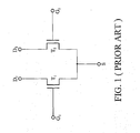
- Fig. 1 is a circuit diagram showing a circuit configuration of a typical differential pair. Two MOS transistors form the differential pair with a common source to multiply the difference between two inputs, G1 and G2, by a predetermined constant, to obtain the differential gain.
- Fig. 2 further illustrates the layout of the differential pair and shows an example of a conventional circuit layout of the typical differential pair.
- the transistor T1 includes gate fingers G22 to G24 electrically connected to a gate wire W G1 , drain fingers D22 and D23 electrically connected to a drain wire W D1 , and source fingers S22 and S23 electrically connected to a source line W S1 .
- the transistor T1 further comprises a guard ring 21a coupled to the body of the transistor T1.
- the transistor T2 includes gate fingers G25 to G27 electrically connected to a gate wire W G2 , drain fingers D25 and D26 electrically connected to a drain wire W D2 , and source fingers S25 and S26 electrically connected to a source line W S2 .
- the transistor T2 further comprises a guard ring 21b coupled to the body of the transistor T2.
- the differential pair occupies too much layout area, easily generating large parasitic capacitance due to the metal connection.
- a differential pair configuration of an integrated circuit for reducing layout area and parasitic capacitance is provided.
- An exemplary embodiment of an integrated circuit device comprises a first MOS formed by a multiple fingers configuration, having a plurality of first gate fingers; a second MOS formed by the multiple fingers configuration, having a plurality of second gate fingers, wherein each two first gate fingers interdigitate with each two second gate fingers.
- Another exemplary embodiment of the integrated circuit device comprises a plurality of first gate fingers; a plurality of second gate fingers, wherein each two first gate fingers interdigitate with each two second gate fingers; a plurality of first drain fingers formed between each two first gate fingers; a plurality of second drain fingers formed between each two second gate fingers; a plurality of common source fingers formed between one first gate finger and one second gate finger.
- the integrated circuit device comprises a first differential pair and a second differential pair.
- the first differential pair comprises a first drain finger coupled to a first drain wire, a first gate finger coupled to a first gate wire, a first source finger coupled to a common source wire, a second gate finger coupled to a second gate wire, and a second drain finger coupled to a second drain wire.
- the second differential pair comprises a third drain finger coupled to the first drain wire, a third gate finger coupled to the first gate wire, a second source finger coupled to the common source wire, a fourth gate finger coupled to the second gate wire, and a fourth drain finger coupled to the second drain wire.
- Fig. 1 is a circuit diagram showing a circuit configuration of a typical differential pair.
- Fig. 2 shows an example of a conventional circuit layout of the typical differential pair.
- Fig. 3 shows a circuit layout of an embodiment of the differential pair.
- Fig. 4 is a cross section view of the differential pair in Fig. 3 .
- Fig. 5 shows a circuit layout of another embodiment of the differential pair.
- the differential pair relating of the invention has a circuit configuration as shown in Fig. 1 , and is characterized by a circuit layout of the transistors, T1 and T2.
- Fig. 3 shows a circuit layout of an embodiment of the differential pair.
- the transistors T1 and T2 both have a multiple finger configuration.
- the transistor T1 has drain fingers D31 to D34 (D31, D32, D33 and D34) electrically connected to a drain wire W D1 , and gate fingers G31a to G37a (G31a, G32a, G33a, G34a, G35a, G36a and G37a) electrically connected to a gate line W G1 .
- the transistor T2 has drain fingers D35 to D38 (D35, D36, D37 and D38) electrically connected to a drain wire W D2 , and gate fingers G31b to G37b (G31b, G32b, G33b, G34b, G35b, G36b and G37b) electrically connected to a gate line W G2 .
- the transistors T1 and T2 share source fingers S31 to S37 (S31, S32, S33, S34, S35, S36 and S37) electrically connected to a source line W s .
- the source line W s can be connected to a virtual ground.
- the guard ring 31 is coupled to both the bodies of the transistors T1 and T2.
- each two gate fingers of transistor T1 interdigitate with each two gate fingers of transistor T2.
- the drain fingers D31 to D34 are disposed between two gate fingers of transistor T1.
- the drain fingers D35 to D38 are disposed between two gate fingers of transistor T2.
- the source fingers S31 to S37 are disposed between one gate finger of transistor T1 and one gate finger of transistor T2. According to the differential pair configuration shown in Fig. 3 , the layout area can be reduced and the source parasitic capacitance also can be reduced due to the shared source and guard ring.
- differential pair circuit of the invention can be utilized in integrated circuit devices operated in high frequency, such as RF devices.
- Fig. 4 is a cross sectional view of the differential pair shown in Fig. 3 .
- drain fingers D31 and D32, gate fingers G31a and G37b, and source fingers S31 and S32 are shown, others have similar structure.
- a p+ region is doped on a P-substrate 41 to form the guard ring 31.
- the two differential pair configurations are divided by a shallow trench isolation (STI) doped on the P-substrate.
- a plurality of n+ regions is doped on the P-substrate 41 to form source fingers and drain fingers.
- STI shallow trench isolation
- the fingers including gate fingers, drain fingers, and source fingers are formed by a conductive layer, such as conductive layer 44, and a metal contact pad, such as metal contact pad 45.
- the remaining space, with the exception of the conductive layer and metal contact pad, is filled with isolation material.
- the metal contact pads of the source fingers are not disposed in the same layer in which metal contact pads of the drain fingers and gate fingers are disposed.
- an isolation layer 42 covers the metal contact pads.
- a plurality of vias, such as via 43, is then formed by perforating the isolation layer 42 based on the position of source fingers and filled with conductive material.
- the metal contact pads are then formed on the vias. According to the configuration shown in Fig. 4 , the source parasitic capacitance can be efficiently reduced and the differential pair obtains better matching of the transistors T1 and T2.
- Fig. 5 shows a circuit layout of another embodiment of the differential pair.
- the transistors T1 and T2 both have a multiple finger configuration.
- the transistor T1 has drain fingers D51, D52, D53 and D54 electrically connected to a drain wire W D1 , and gate fingers G51, G52, G53 and G54 electrically connected to a gate line W G1 .
- the transistor T2 has drain fingers D55, D56, D57 and D58 electrically connected to a drain wire W D2 , and gate fingers G55, G56, G57 and G58 electrically connected to a gate line W G2 .
- the transistors T1 and T2 share source fingers S51, S52, S53, and S54 electrically connected to a source line W s .
- the source line W s can be connected to a virtual ground.
- a guard ring 51 is provided and is coupled to both the bodies of the transistors T1 and T2.
- the differential pair comprises plural differential pair units, such as the differential pair unit formed by the drain finger D51, the gate finger G51, the source finger S51, the gate finger G55, and the drain finger D55.
- the differential pair comprises four differential pair units, and in another embodiment, the differential pair may only comprise one differential pair unit.
- the advantage of the configuration shown in Fig. 5 is that the source parasitic capacitance can be reduced due to the shared source and guard ring.
Landscapes
- Semiconductor Integrated Circuits (AREA)
- Amplifiers (AREA)
Applications Claiming Priority (1)
| Application Number | Priority Date | Filing Date | Title |
|---|---|---|---|
| US11/616,489 US20080157222A1 (en) | 2006-12-27 | 2006-12-27 | Rf integrated circuit device |
Publications (2)
| Publication Number | Publication Date |
|---|---|
| EP1939940A2 true EP1939940A2 (fr) | 2008-07-02 |
| EP1939940A3 EP1939940A3 (fr) | 2009-06-10 |
Family
ID=39243708
Family Applications (1)
| Application Number | Title | Priority Date | Filing Date |
|---|---|---|---|
| EP07101698A Withdrawn EP1939940A3 (fr) | 2006-12-27 | 2007-02-02 | Dispositif de circuit intégré RF |
Country Status (4)
| Country | Link |
|---|---|
| US (1) | US20080157222A1 (fr) |
| EP (1) | EP1939940A3 (fr) |
| CN (1) | CN101211916A (fr) |
| TW (1) | TW200828841A (fr) |
Cited By (2)
| Publication number | Priority date | Publication date | Assignee | Title |
|---|---|---|---|---|
| EP4086946A1 (fr) * | 2021-05-03 | 2022-11-09 | C2Amps AB | Structure semi-conductrice formant une pluralité de transistors |
| TWI921529B (zh) | 2021-05-03 | 2026-04-11 | 瑞典商C2安培公司 | 形成多個電晶體的半導體結構 |
Families Citing this family (28)
| Publication number | Priority date | Publication date | Assignee | Title |
|---|---|---|---|---|
| SE526360C2 (sv) * | 2004-01-09 | 2005-08-30 | Infineon Technologies Ag | Monolitiskt integrerad krets |
| US20080251863A1 (en) * | 2007-04-14 | 2008-10-16 | Sheng-Yi Huang | High-voltage radio-frequency power device |
| JP2010045133A (ja) * | 2008-08-11 | 2010-02-25 | Toshiba Corp | 半導体集積回路装置 |
| CN101764136B (zh) * | 2009-12-24 | 2011-11-16 | 中国科学院上海微系统与信息技术研究所 | 一种可调节垂直栅soi cmos器件沟道电流的叉指型结构 |
| CN102169895A (zh) * | 2010-02-25 | 2011-08-31 | 上海北京大学微电子研究院 | 射频金属-氧化物-半导体场效应晶体管 |
| JP5397289B2 (ja) * | 2010-03-29 | 2014-01-22 | 住友電気工業株式会社 | 電界効果トランジスタ |
| CN102651365B (zh) * | 2011-02-25 | 2015-03-11 | 晶豪科技股份有限公司 | 集成电路结构 |
| US9721936B2 (en) | 2013-08-07 | 2017-08-01 | Skyworks Solutions, Inc. | Field-effect transistor stack voltage compensation |
| US9620424B2 (en) | 2013-11-12 | 2017-04-11 | Skyworks Solutions, Inc. | Linearity performance for radio-frequency switches |
| US11901243B2 (en) * | 2013-11-12 | 2024-02-13 | Skyworks Solutions, Inc. | Methods related to radio-frequency switching devices having improved voltage handling capability |
| US9324819B1 (en) * | 2014-11-26 | 2016-04-26 | Delta Electronics, Inc. | Semiconductor device |
| US12464760B2 (en) | 2016-03-17 | 2025-11-04 | Macom Technology Solutions Holdings, Inc. | Bypassed gate transistors having improved stability |
| US9947616B2 (en) * | 2016-03-17 | 2018-04-17 | Cree, Inc. | High power MMIC devices having bypassed gate transistors |
| US10128365B2 (en) | 2016-03-17 | 2018-11-13 | Cree, Inc. | Bypassed gate transistors having improved stability |
| US10410957B2 (en) * | 2016-03-31 | 2019-09-10 | Skyworks Solutions, Inc. | Body contacts for field-effect transistors |
| US9960127B2 (en) | 2016-05-18 | 2018-05-01 | Macom Technology Solutions Holdings, Inc. | High-power amplifier package |
| US10134658B2 (en) * | 2016-08-10 | 2018-11-20 | Macom Technology Solutions Holdings, Inc. | High power transistors |
| JP6812764B2 (ja) * | 2016-11-29 | 2021-01-13 | 日亜化学工業株式会社 | 電界効果トランジスタ |
| US10978583B2 (en) | 2017-06-21 | 2021-04-13 | Cree, Inc. | Semiconductor devices having a plurality of unit cell transistors that have smoothed turn-on behavior and improved linearity |
| US10615273B2 (en) | 2017-06-21 | 2020-04-07 | Cree, Inc. | Semiconductor devices having a plurality of unit cell transistors that have smoothed turn-on behavior and improved linearity |
| US10700063B2 (en) * | 2017-12-31 | 2020-06-30 | Skyworks Solutions, Inc. | Devices and methods for layout-dependent voltage handling improvement in switch stacks |
| US10763334B2 (en) | 2018-07-11 | 2020-09-01 | Cree, Inc. | Drain and/or gate interconnect and finger structure |
| US10483352B1 (en) | 2018-07-11 | 2019-11-19 | Cree, Inc. | High power transistor with interior-fed gate fingers |
| US10600746B2 (en) | 2018-07-19 | 2020-03-24 | Cree, Inc. | Radio frequency transistor amplifiers and other multi-cell transistors having gaps and/or isolation structures between groups of unit cell transistors |
| US10629526B1 (en) * | 2018-10-11 | 2020-04-21 | Nxp Usa, Inc. | Transistor with non-circular via connections in two orientations |
| US10770415B2 (en) | 2018-12-04 | 2020-09-08 | Cree, Inc. | Packaged transistor devices with input-output isolation and methods of forming packaged transistor devices with input-output isolation |
| US11417746B2 (en) * | 2019-04-24 | 2022-08-16 | Wolfspeed, Inc. | High power transistor with interior-fed fingers |
| EP4264666A1 (fr) * | 2021-01-11 | 2023-10-25 | Huawei Technologies Co., Ltd. | Transistor de puissance multi-terminal au nitrure de gallium |
Family Cites Families (7)
| Publication number | Priority date | Publication date | Assignee | Title |
|---|---|---|---|---|
| JPS62150779A (ja) * | 1985-12-25 | 1987-07-04 | Hitachi Ltd | 半導体装置 |
| JPH088264B2 (ja) * | 1988-06-30 | 1996-01-29 | 株式会社東芝 | 半導体集積回路 |
| JP2557561B2 (ja) * | 1990-10-09 | 1996-11-27 | 三菱電機株式会社 | 半導体装置 |
| US7221011B2 (en) * | 2001-09-07 | 2007-05-22 | Power Integrations, Inc. | High-voltage vertical transistor with a multi-gradient drain doping profile |
| US7015545B2 (en) * | 2002-03-18 | 2006-03-21 | Broadcom Corporation | Split source RF MOSFET device |
| US7079829B2 (en) * | 2002-11-15 | 2006-07-18 | Matsushita Electric Industrial Co, Ltd. | Semiconductor differential circuit, oscillation apparatus, switching apparatus, amplifying apparatus, mixer apparatus and circuit apparatus using same, and semiconductor differential circuit placement method |
| US6798022B1 (en) * | 2003-03-11 | 2004-09-28 | Oki Electric Industry Co., Ltd. | Semiconductor device with improved protection from electrostatic discharge |
-
2006
- 2006-12-27 US US11/616,489 patent/US20080157222A1/en not_active Abandoned
-
2007
- 2007-02-02 EP EP07101698A patent/EP1939940A3/fr not_active Withdrawn
- 2007-07-30 TW TW096127743A patent/TW200828841A/zh unknown
- 2007-08-10 CN CNA2007101403705A patent/CN101211916A/zh active Pending
Cited By (3)
| Publication number | Priority date | Publication date | Assignee | Title |
|---|---|---|---|---|
| EP4086946A1 (fr) * | 2021-05-03 | 2022-11-09 | C2Amps AB | Structure semi-conductrice formant une pluralité de transistors |
| WO2022233734A1 (fr) * | 2021-05-03 | 2022-11-10 | C2Amps Ab | Structure semi-conductrice formant une pluralité de transistors |
| TWI921529B (zh) | 2021-05-03 | 2026-04-11 | 瑞典商C2安培公司 | 形成多個電晶體的半導體結構 |
Also Published As
| Publication number | Publication date |
|---|---|
| US20080157222A1 (en) | 2008-07-03 |
| EP1939940A3 (fr) | 2009-06-10 |
| CN101211916A (zh) | 2008-07-02 |
| TW200828841A (en) | 2008-07-01 |
Similar Documents
| Publication | Publication Date | Title |
|---|---|---|
| EP1939940A2 (fr) | Dispositif de circuit intégré RF | |
| US8212311B2 (en) | Semiconductor device having increased gate length implemented by surround gate transistor arrangements | |
| US9755068B2 (en) | Semiconductor device and radio frequency module formed on high resistivity substrate | |
| US20210013253A1 (en) | Electronic device | |
| US8058694B2 (en) | Semiconductor device | |
| US20130249055A1 (en) | Semiconductor capacitor | |
| US20080237705A1 (en) | Ldmos Transistor | |
| US20080251863A1 (en) | High-voltage radio-frequency power device | |
| US20150129977A1 (en) | Semiconductor electrostatic discharge protection apparatus | |
| US8324710B2 (en) | Capacitor, integrated device, radio frequency switching device, and electronic apparatus | |
| US10217740B2 (en) | Semiconductor device and radio frequency module formed on high resistivity substrate | |
| US9640551B2 (en) | Passive device and radio frequency module formed on high resistivity substrate | |
| US9385246B2 (en) | Differential MOSCAP device | |
| US7977709B2 (en) | MOS transistor and semiconductor device | |
| US7969239B2 (en) | Charge pump circuit and a novel capacitor for a memory integrated circuit | |
| US11521967B2 (en) | Multi-finger devices with reduced parasitic capacitance | |
| US9972673B2 (en) | Electrostatic discharge protection device | |
| US20230187144A1 (en) | Capacitor structure and semiconductor device | |
| US7642615B2 (en) | Semiconductor device with a noise prevention structure | |
| US7417277B2 (en) | Semiconductor integrated circuit and method of manufacturing the same | |
| US7285837B2 (en) | Electrostatic discharge device integrated with pad | |
| US8981488B1 (en) | Semiconductor structure and integrated circuit | |
| JP5372578B2 (ja) | 半導体装置 | |
| JP2007019413A (ja) | 保護回路用半導体装置 | |
| US20230420492A1 (en) | Semiconductor structure |
Legal Events
| Date | Code | Title | Description |
|---|---|---|---|
| PUAI | Public reference made under article 153(3) epc to a published international application that has entered the european phase |
Free format text: ORIGINAL CODE: 0009012 |
|
| AK | Designated contracting states |
Kind code of ref document: A2 Designated state(s): AT BE BG CH CY CZ DE DK EE ES FI FR GB GR HU IE IS IT LI LT LU LV MC NL PL PT RO SE SI SK TR |
|
| AX | Request for extension of the european patent |
Extension state: AL BA HR MK RS |
|
| PUAL | Search report despatched |
Free format text: ORIGINAL CODE: 0009013 |
|
| AK | Designated contracting states |
Kind code of ref document: A3 Designated state(s): AT BE BG CH CY CZ DE DK EE ES FI FR GB GR HU IE IS IT LI LT LU LV MC NL PL PT RO SE SI SK TR |
|
| AX | Request for extension of the european patent |
Extension state: AL BA HR MK RS |
|
| AKX | Designation fees paid | ||
| STAA | Information on the status of an ep patent application or granted ep patent |
Free format text: STATUS: THE APPLICATION IS DEEMED TO BE WITHDRAWN |
|
| 18D | Application deemed to be withdrawn |
Effective date: 20091211 |
|
| REG | Reference to a national code |
Ref country code: DE Ref legal event code: 8566 |