EP1939942A2 - Halbleiterbauelement und Herstellungsverfahren dafür - Google Patents
Halbleiterbauelement und Herstellungsverfahren dafür Download PDFInfo
- Publication number
- EP1939942A2 EP1939942A2 EP07150240A EP07150240A EP1939942A2 EP 1939942 A2 EP1939942 A2 EP 1939942A2 EP 07150240 A EP07150240 A EP 07150240A EP 07150240 A EP07150240 A EP 07150240A EP 1939942 A2 EP1939942 A2 EP 1939942A2
- Authority
- EP
- European Patent Office
- Prior art keywords
- fins
- pair
- insulating layer
- forming
- outer surfaces
- Prior art date
- Legal status (The legal status is an assumption and is not a legal conclusion. Google has not performed a legal analysis and makes no representation as to the accuracy of the status listed.)
- Withdrawn
Links
Images


Classifications
-
- H—ELECTRICITY
- H10—SEMICONDUCTOR DEVICES; ELECTRIC SOLID-STATE DEVICES NOT OTHERWISE PROVIDED FOR
- H10D—INORGANIC ELECTRIC SEMICONDUCTOR DEVICES
- H10D30/00—Field-effect transistors [FET]
- H10D30/60—Insulated-gate field-effect transistors [IGFET]
- H10D30/62—Fin field-effect transistors [FinFET]
-
- H—ELECTRICITY
- H10—SEMICONDUCTOR DEVICES; ELECTRIC SOLID-STATE DEVICES NOT OTHERWISE PROVIDED FOR
- H10P—GENERIC PROCESSES OR APPARATUS FOR THE MANUFACTURE OR TREATMENT OF DEVICES COVERED BY CLASS H10
- H10P10/00—Bonding of wafers, substrates or parts of devices
-
- H—ELECTRICITY
- H10—SEMICONDUCTOR DEVICES; ELECTRIC SOLID-STATE DEVICES NOT OTHERWISE PROVIDED FOR
- H10D—INORGANIC ELECTRIC SEMICONDUCTOR DEVICES
- H10D30/00—Field-effect transistors [FET]
- H10D30/01—Manufacture or treatment
- H10D30/021—Manufacture or treatment of FETs having insulated gates [IGFET]
- H10D30/024—Manufacture or treatment of FETs having insulated gates [IGFET] of fin field-effect transistors [FinFET]
-
- H—ELECTRICITY
- H10—SEMICONDUCTOR DEVICES; ELECTRIC SOLID-STATE DEVICES NOT OTHERWISE PROVIDED FOR
- H10D—INORGANIC ELECTRIC SEMICONDUCTOR DEVICES
- H10D30/00—Field-effect transistors [FET]
- H10D30/01—Manufacture or treatment
- H10D30/021—Manufacture or treatment of FETs having insulated gates [IGFET]
- H10D30/0411—Manufacture or treatment of FETs having insulated gates [IGFET] of FETs having floating gates
-
- H—ELECTRICITY
- H10—SEMICONDUCTOR DEVICES; ELECTRIC SOLID-STATE DEVICES NOT OTHERWISE PROVIDED FOR
- H10D—INORGANIC ELECTRIC SEMICONDUCTOR DEVICES
- H10D30/00—Field-effect transistors [FET]
- H10D30/01—Manufacture or treatment
- H10D30/021—Manufacture or treatment of FETs having insulated gates [IGFET]
- H10D30/0413—Manufacture or treatment of FETs having insulated gates [IGFET] of FETs having charge-trapping gate insulators, e.g. MNOS transistors
-
- H—ELECTRICITY
- H10—SEMICONDUCTOR DEVICES; ELECTRIC SOLID-STATE DEVICES NOT OTHERWISE PROVIDED FOR
- H10D—INORGANIC ELECTRIC SEMICONDUCTOR DEVICES
- H10D30/00—Field-effect transistors [FET]
- H10D30/60—Insulated-gate field-effect transistors [IGFET]
- H10D30/62—Fin field-effect transistors [FinFET]
- H10D30/6219—Fin field-effect transistors [FinFET] characterised by the source or drain electrodes
-
- H—ELECTRICITY
- H10—SEMICONDUCTOR DEVICES; ELECTRIC SOLID-STATE DEVICES NOT OTHERWISE PROVIDED FOR
- H10D—INORGANIC ELECTRIC SEMICONDUCTOR DEVICES
- H10D30/00—Field-effect transistors [FET]
- H10D30/60—Insulated-gate field-effect transistors [IGFET]
- H10D30/68—Floating-gate IGFETs
- H10D30/681—Floating-gate IGFETs having only two programming levels
-
- H—ELECTRICITY
- H10—SEMICONDUCTOR DEVICES; ELECTRIC SOLID-STATE DEVICES NOT OTHERWISE PROVIDED FOR
- H10D—INORGANIC ELECTRIC SEMICONDUCTOR DEVICES
- H10D30/00—Field-effect transistors [FET]
- H10D30/60—Insulated-gate field-effect transistors [IGFET]
- H10D30/69—IGFETs having charge trapping gate insulators, e.g. MNOS transistors
-
- H—ELECTRICITY
- H10—SEMICONDUCTOR DEVICES; ELECTRIC SOLID-STATE DEVICES NOT OTHERWISE PROVIDED FOR
- H10W—GENERIC PACKAGES, INTERCONNECTIONS, CONNECTORS OR OTHER CONSTRUCTIONAL DETAILS OF DEVICES COVERED BY CLASS H10
- H10W20/00—Interconnections in chips, wafers or substrates
- H10W20/01—Manufacture or treatment
- H10W20/031—Manufacture or treatment of conductive parts of the interconnections
- H10W20/069—Manufacture or treatment of conductive parts of the interconnections by forming self-aligned vias or self-aligned contact plugs
-
- H—ELECTRICITY
- H10—SEMICONDUCTOR DEVICES; ELECTRIC SOLID-STATE DEVICES NOT OTHERWISE PROVIDED FOR
- H10D—INORGANIC ELECTRIC SEMICONDUCTOR DEVICES
- H10D30/00—Field-effect transistors [FET]
- H10D30/60—Insulated-gate field-effect transistors [IGFET]
- H10D30/62—Fin field-effect transistors [FinFET]
- H10D30/6211—Fin field-effect transistors [FinFET] having fin-shaped semiconductor bodies integral with the bulk semiconductor substrates
Definitions
- Example embodiments relate to a semiconductor device and method of fabrication the same.
- Other example embodiments relate to a semiconductor device including a fin-type channel region and a method of fabricating the same.
- a highly integrated semiconductor device which uses a fin field effect transistor (FinFET) or a fin memory cell, may increase the area of a channel in order to increase an operating speed of the semiconductor device and/or decrease a width of the fin in order to increase an integration density of the semiconductor device.
- FinFET fin field effect transistor
- the conventional art acknowledges a FinFET and a fin memory cell.
- the conventional art also acknowledges a FinFET using a silicon-on-insulator (SOI) substrate.
- SOI silicon-on-insulator
- the conventional FinFET and fin memory cells may have problems associated with the stability of thin fin structures. It may be difficult to form uniform contact plugs in the fin structures. It may be difficult to decrease a contact resistance between the thin fin structures and the contact plugs.
- Example embodiments relate to a semiconductor device and method of fabrication the same.
- Other example embodiments relate to a semiconductor device including a fin-type channel region and a method of fabricating the same.
- Example embodiments relate a semiconductor device that may increase the stability of a fin structure and/or the reliability of a contact plug and a method of fabricating the same.
- a semiconductor device including a semiconductor substrate, a semiconductor pillar and a contact plug.
- the semiconductor substrate includes at least one pair of fins used (or functioning) as an active region.
- the semiconductor pillar may be interposed (or formed) between portions of the fins to connect the fins.
- the contact plug may be disposed (or formed) on the semiconductor pillar. The contact plug may electrically connect to top surfaces of the fins.
- the fins and the semiconductor pillar may be formed of the same semiconductor material.
- the semiconductor substrate may include a bulk semiconductor wafer.
- the fins and the semiconductor pillar may be formed by etching the bulk semiconductor wafer.
- the semiconductor device may include a buried insulating layer interposed (or formed) between the fins and the semiconductor pillar.
- the semiconductor device may include a bridge insulating layer for connecting top ends of the fins to define a void between the fins and the semiconductor pillar.
- the semiconductor device may include a gate electrode extending (or formed) across the buried insulating layer and/or covering (or formed on) portions of outer surfaces of the fins on an opposite side of the fins than the buried insulating layer.
- a gate insulating layer may be interposed (or formed) between the outer surfaces of the fins and the gate electrode.
- a method of fabricating a semiconductor device includes forming a device isolation layer on a semiconductor substrate to define an active region.
- the active region may be etched to form at least one pair of fins and a semiconductor pillar such that the semiconductor pillar is interposed between portions of the fins in order to connect the fins.
- a contact plug may be formed on the semiconductor pillar such that the contact plug is electrically connected to top surfaces of the fins.
- FIGS. 1-9 represent non-limiting, example embodiments as described herein.
- first, second, third etc. may be used herein to describe various elements, components, regions, layers and/or sections, these elements, components, regions, layers and/or sections should not be limited by these terms. These terms are only used to distinguish one element, component, region, layer or section from another region, layer or section. Thus, a first element, component, region, layer or section discussed below could be termed a second element, component, region, layer or section without departing from the scope of example embodiments.
- spatially relative terms such as “beneath,” “below,” “lower,” “above,” “upper” and the like, may be used herein for ease of description to describe one element or a relationship between a feature and another element or feature as illustrated in the figures. It will be understood that the spatially relative terms are intended to encompass different orientations of the device in use or operation in addition to the orientation depicted in the Figures. For example, if the device in the figures is turned over, elements described as “below” or “beneath” other elements or features would then be oriented “above” the other elements or features. Thus, for example, the term “below” can encompass both an orientation which is above as well as below. The device may be otherwise oriented (rotated 90 degrees or viewed or referenced at other orientations) and the spatially relative descriptors used herein should be interpreted accordingly.
- Example embodiments are described herein with reference to cross-sectional illustrations that are schematic illustrations of idealized embodiments (and intermediate structures). As such, variations from the shapes of the illustrations as a result, for example, of manufacturing techniques and/or tolerances, may be expected. Thus, example embodiments should not be construed as limited to the particular shapes of regions illustrated herein but may include deviations in shapes that result, for example, from manufacturing. For example, an implanted region illustrated as a rectangle may have rounded or curved features and/or a gradient (e.g., of implant concentration) at its edges rather than an abrupt change from an implanted region to a non-implanted region.
- a gradient e.g., of implant concentration
- a buried region formed by implantation may result in some implantation in the region between the buried region and the surface through which the implantation may take place.
- the regions illustrated in the figures are schematic in nature and their shapes do not necessarily illustrate the actual shape of a region of a device and do not limit the scope.
- Example embodiments relate to a semiconductor device and method of fabrication the same.
- Other example embodiments relate to a semiconductor device including a fin-type channel region and a method of fabricating the same.
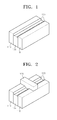
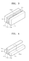
- FIGS. 1 through 5 are diagrams illustrating perspective views of a semiconductor device and a method of fabricating the same according to example embodiments.
- the semiconductor device according to example embodiments may be referred to as a fin field effect transistor (Fin-FET).
- Fin-FET fin field effect transistor
- example embodiments are not limited thereto.
- the semiconductor device may be formed with a semiconductor substrate (not shown) including a pair of fins 105a and 105b.
- the fins 105a and 105b may be used (or function) as an active region.
- the active region may be defined by a device isolation layer 110.
- the semiconductor substrate may include a body 105c for connecting the bottom ends of the fins 105a and 105b.
- a semiconductor pillar 105d may be interposed between the fins 105a and 105b to connect portions of the fins 105a and 105b.
- the semiconductor pillar 105d may be used to fix and/or support the fins 105a and 105b. If the fins 105a and 105b are formed of a thin layer, the fins 105a and 105b may be stabilized on the body 105c due to the semiconductor pillar 105d. A reduction in the widths of the fins 105a and 105b may increase the integration density of the semiconductor device.
- the fins 105a and 105b, the semiconductor pillar 105d and the body 105c may be formed of the same semiconductor material.
- a bulk semiconductor wafer may be etched to define the fins 105a and 105b, the semiconductor pillar 105d and/or the body 105c in the semiconductor substrate.
- the bulk semiconductor wafer may be a silicon wafer, a germanium wafer or a silicon-germanium wafer.
- any two (or all) of the fins 105a and 105b, the semiconductor pillar 105d and the body 105c may be formed of different semiconductor materials.
- the body 105c may be formed of a single-crystalline wafer and the fins 105a and 105c and the semiconductor pillar 105d may be formed of a semiconductor epitaxial layer.
- a contact plug 150 may be disposed (or formed) on the semiconductor pillar 105d.
- the contact plug 150 may be electrically connected to the top ends of the fins 105a and 105b. If the fins 105a and 105b are thin, it may be difficult to form the contact plug 150 directly on the top surfaces of the fins 105a and 105b. Because the semiconductor pillar 105d is interposed between the fins 105a and 105b, the contact plug 150 may be more uniformly and stably formed on the top ends of the fins 105a and 105b.
- the contact plug 150 may be aligned with the top surfaces of the fins 105a and 105b, the contact plug 150 may not penetrate between the fins 105a and 105b. Because the contact plug 150 may be aligned with the top surfaces of the fins 105a and 105b, the contact plug 150 may not damage the fins 105a and 105b. If the contact plug 150 is in contact with lateral surfaces of the fins 105a and 105b, the fins 105a and 105b may be damaged by the contact plug 150.
- a contact resistance between the contact plug 150 and the fins 105a and 105b may decrease.
- the process of forming a metal silicide layer or a metal salicide layer on the top ends of the thin fins 105a and 105b without the semiconductor pillar 105d may be difficult.
- the formation of a metal salicide layer involves wet etching an unreacted metal. It may be difficult to perform a selective wet etching process between the thin fins 105a and 105b.
- At least one MOS transistor may be selectively formed using the fins 105a and 105b as a channel region.
- a buried insulating layer 130 may be interposed (or formed) between the fins 105a and 105b and the semiconductor pillar 105d.
- the outer lateral surfaces of the fins 105a and 105b on the opposite side to the buried insulating layer 130 may function as a channel region. Because lower portions of the outer surfaces of the fins 105a and 105b may be covered with the device isolation layer 110, the upper portions of the outer surfaces of the fins 105a and 105b may be used as the channel region. According to other example embodiments, only the upper portions of the outer surfaces of the fins 105a and 105b may be used as the channel region.
- a gate electrode 145 may extend across the buried insulating layer 130.
- the gate electrode 145 may cover at least the upper portions of the outer surfaces of the fins 105a and 105b.
- Gate insulating layers 140 may be interposed (or formed) between the gate electrode 145 and the outer surfaces of the fins 105a and 105b. According to example embodiments, the gate insulating layers 140 may be connected to one another across the fins 105a and 105b.
- the contact plug 150 may be connected to a common source and/or drain electrode.
- the contact plug 150 may be connected to common source or drain regions (not shown) of the fins 105a and 105b.
- the number of semiconductor pillars 105d and contact plugs 150 is not limited to the above example embodiments.
- the number of semiconductor pillars 105d and contact plugs 150 may be selected according to the type of a semiconductor device.
- the MOS transistor may be used to increase the area of a channel region and/or an operating current.
- the MOS transistor may be used to form an inverter having a common source or drain electrode.
- example embodiments have been described with reference to a pair of fins 105a and 105b. However, example embodiments are not limited thereto.
- a plurality of fins may be disposed (or formed) and semiconductor pillars may be interposed between two of the fins.
- the semiconductor substrate may include an active region 105 defined by device isolation layers 110.
- the semiconductor substrate may extend under the active region 105.
- the semiconductor substrate may support the device isolation layers 110.
- the device isolation layers 110 may be formed by etching a bulk semiconductor wafer so that the active region 105 may be defined between the device isolation layers 110.
- the device isolation layers 110 may be formed using an oxide layer.
- the active region 105 may be formed of a semiconductor epitaxial layer.
- the semiconductor substrate may include a single-crystalline bulk semiconductor wafer (not shown) disposed under the active region 105.
- a pair of spacer insulating layers 115 may be formed on the sidewalls at the top ends of the device isolation layers 110.
- the spacer insulating layers 115 may be formed to cover (or over) both edges of the active region 105.
- the spacer insulating layers 115 may be formed using a nitride layer.
- a mask layer 120 may be formed covering (or over) a portion of the active region 105.
- the mask layer 120 may be formed intersecting the spacer insulating layers 115.
- the mask layer 120 may be formed using a photoresist layer, an oxide layer or a nitride layer.
- an exposed portion of the active region 105 may be etched using the spacer insulating layers 115 and the mask layer 120 as etch protection layers.
- a pair of fins 105a and 105b may be formed on a body 105c.
- a semiconductor pillar 105d may be formed on the fins 105a and 105b.
- the width of the fins 105a and 105b may be controlled by adjusting the width of the spacer insulating layers 115.
- the body 105c may connect the bottom ends of the fins 105a and 105b to each other.
- the body 105c may be the remaining portion of the semiconductor substrate (except the fins 105a and 105b and the semiconductor pillar 105d).
- the semiconductor pillar 105d may correspond to a portion of the active region 105 disposed (or formed) under the mask layer 120.
- the semiconductor pillar 105d may be disposed (or formed) on a portion of the active region 105 between the fins 105a and 105b to connect the fins 105a and 105b.
- the fins 105a and 105b, the semiconductor pillar 105d and the body 105c may be formed by etching the same semiconductor material.
- the fins 105a and 105b, the semiconductor pillar 105d and the body 105c may be formed of different semiconductor materials.
- the fins 105a and 105b and the semiconductor pillar 105d may be formed simultaneously by etching the active region 105 using an appropriate mask layer (not shown). If the fins 105a and 105b have a small width, it may be difficult to form the mask layer.
- the spacer insulating layers 115 may be removed.
- a buried insulating layer 130 may be formed between the fins 105a and 105b and the semiconductor pillar 105d.
- the buried insulating layer 130 may be obtained (or formed) by forming an insulating layer using a chemical vapor deposition (CVD) process and planarizing the insulating layer.
- the buried insulating layer 130 may be formed using a nitride layer.
- the spacer insulating layers 115 may not be removed.
- the buried insulating layer 130 may be formed on the spacer insulating layers 115.
- the device isolation layer 110 may be etched to a desired height using the buried insulating layer 130 as an etch protection layer. Upper portions of the outer surfaces of the fins 105a and 105b, which are disposed (or formed) on the opposite side of the fins 105a and 105b than the buried insulating layer 130, may be exposed.
- gate insulating layers 140 may be formed covering the upper portions of the outer surfaces of the fins 105a and 105b.
- the gate insulating layers 140 may be formed by oxidizing the exposed surfaces of the fins 105a and 105b.
- the gate insulating layers 140 may be formed using a CVD process.
- the gate insulating layers 140 may be connected to each another across the buried insulating layer 130.
- a gate electrode 145 may extend across the buried insulating layer 130 and/or cover the gate insulating layers 140.
- the gate electrode 145 may be obtained (or formed) by forming a polysilicon layer, a metal layer or a metal silicide layer. A resulting layer may be patterned.
- a portion of the buried insulating layer 130 may be etched, forming a contact hole (not shown) exposing portions of top surfaces of the fins 105a and 105b and a top surface of the semiconductor pillar 105d.
- a contact plug 150 may be formed such that the contact plug 150 is connected to the top surfaces of the fins 105a and 105b.
- the contact plug 150 may be mounted on the semiconductor pillar 105d.
- the contact plug 150 may be obtained (or formed) by forming a polysilicon layer, a metal layer or a metal silicide layer. A resulting layer may be patterned.
- the semiconductor device may be completed by processes known in the art.
- FIG. 6 is a diagram illustrating a perspective view of a semiconductor device and a method of fabricating the same according to example embodiments.
- the semiconductor device of FIG. 6 is may be formed according to the same method as the semiconductor device of FIG. 5 except that a MOS transistor is replaced by a memory transistor.
- a description of like components in FIGS. 5 and 6 will omitted for the sake of brevity.
- a memory transistor may include a pair of tunneling insulating layers 155, a pair of charge storage layers 160, a blocking insulating layer 165 and a control gate electrode 170.
- the blocking insulating layer 165 may be omitted depending on the type and structure of the charge storage layers 160.
- the memory transistor may be used as a cell for a nonvolatile memory device.
- the tunneling insulating layers 155 may be formed covering (or over) upper portions of outer surfaces of the fins 105a and 105b.
- the tunneling insulating layers 155 may be disposed (or formed) on the opposite side of the fins 105a and 105b than the buried insulating layer 130.
- the control gate electrode 170 may extend across the buried insulating layer 130.
- the control gate electrode 170 may be formed on (or covering) the upper portions of the outer surfaces of the fins 105a and 105b.
- the charge storage layers 160 may be interposed (or formed) between the tunneling insulating layers 155 and the blocking insulating layer 165.
- the blocking insulating layer 165 may be interposed (or formed) between the control gate electrode 170 and the charge storage layers 160.
- the blocking insulating layer 165 may extend over (or across) the buried insulating layer 130.
- the tunneling insulating layers 155 on either side may extend over (or across) the buried insulating layer 130 such that the tunneling insulating layers 155 are connected to one another.
- the charge storage layers 160 on either side may extend over (or across) the buried insulating layer 130 such that the charge storage layers 160 are connected to one another.
- the charge storage layers 160 may have partial charge storage capabilities.
- the tunneling insulating layers 155 and the blocking insulating layer 165 may be formed using an oxide layer, a nitride layer or a high- k dielectric layer.
- the high- k dielectric layer may refer to an insulating layer having a higher dielectric constant than an oxide layer or a nitride layer.
- the charge storage layers 160 may be formed using a polysilicon layer, a nitride layer, quantum dots or nanocrystals.
- the quantum dots or nanocrystals may be formed of a metal or polysilicon.
- the nitride layer, the quantum dots or the nanocrystals may have partial charge storage capability.
- the semiconductor device may be used as a nonvolatile memory device.
- the numbers and structures of the memory transistor and the contact plug 150 may be selected depending on the memory size and structure of the nonvolatile memory device.
- a plurality of fins 105a and 105b may be arranged. If the nonvolatile memory device is a NAND type, the contact plug 150 may be connected to a bit line (not shown). If the nonvolatile memory device is a NOR type, the contact plug 150 may be connected to a source or drain electrode (not shown).
- FIGS. 7 and 8 are diagrams illustrating perspective views of a semiconductor device and a method of fabricating the same according to example embodiments.
- the semiconductor device of FIGS. 7 and 8 may be formed using the same method as the semiconductor device of FIG. 5 except that the buried insulating layer 130 of FIG. 5 is modified. Thus, a description of like components in FIGS. 5 , 7 and 8 will omitted for the sake of brevity.
- a bridge insulating layer 132 may be used instead of the buried insulating layer 130 (refer to FIG. 5 ).
- the bridge insulating layer 132 may be formed on the top ends of the fins 105a and 105b to define a void 135 between the fins 105a and 105b.
- the volume of the void 135 may be controlled by adjusting the position of the bridge insulating layer 132.
- the bridge insulating layer 132 may extend down to upper regions of the fins 105a and 105b.
- the void 135 may have a lower dielectric constant than any insulating material.
- the void 135 may effectively lower a dielectric constant between the fins 105a and 105b. Signal interference between the fins 105a and 105b may be suppressed.
- the semiconductor pillar 105d may define the void 135 in the lengthwise (or horizontal) direction of the fins 105a and 105b.
- the semiconductor pillar 105d may prevent a conductive layer (e.g., a metal layer or a polysilicon layer) from penetrating the void 135. As such, the reliability of the semiconductor device including the void 135 may increase.
- a method of fabricating the semiconductor according to example embodiments may be performed in the same manner as the method of fabricating the semiconductor device as described above with reference to FIGS. 1 through 5 .
- a process of forming the buried insulating layer 130 as described with reference to FIG. 4 may be used instead of a process of forming the bridge insulating layer 132 as described with reference to FIG. 7 .
- the bridge insulating layer 132 may be formed connecting top surfaces of the fins 105a and 105b.
- the void 135 may be defined among the fins 105a and 105b, the semiconductor pillar 105d and the bridge insulating layer 132.
- a MOS transistor and a contact plug 150 may be formed.
- the MOS transistor may be formed by forming the bridge insulating layer 132 instead of the buried insulating layer 130 during the process described with reference to FIG. 5 .
- FIG. 9 is a diagram illustrating perspective view of a semiconductor device and a method of fabricating the same according to example embodiments.
- the semiconductor device of FIG. 9 may be formed by the same method as the semiconductor device of FIG. 6 except that the buried insulating layer 130 of FIG. 6 is modified. Thus, a description of like components in FIGS. 5 and 9 will be omitted for the sake of brevity.
- a bridge insulating layer 132 may be provided instead of the buried insulating layer 130 (refer to FIG. 6 ).
- the bridge insulating layer 132 may define a void 135 between the fins 105a and 105b and the semiconductor pillar 150 in the same manner as described in detail with reference to FIGS. 7 and 8 .
- the void 135 may decrease the interference between memory transistors formed using the fins 105a and 105b.
- a method of fabricating the semiconductor according to example embodiments may be performed in the same manner as the method of fabricating the semiconductor device as described above with reference to FIGS. 1 through 4 and 6 .
- a process of forming the buried insulating layer 130 as described with reference to FIG. 4 may be used instead of a process of forming the bridge insulating layer 132 as described with reference to FIG. 7 .
- a memory transistor and a contact plug 150 may be formed.
- the memory transistor may be formed by forming the bridge insulating layer 132 instead of the buried insulating layer 130 during the process described with reference to FIG. 6 .
- a semiconductor device includes a semiconductor pillar interposed between fins such that a contact plug may be more uniformly and stably formed on the top ends of the fins.
- a metal silicide layer or a metal salicide layer may be formed on the surfaces of the semiconductor pillar and the fins, decreasing a contact resistance between the contact plug and the fins.
- expansion of a void disposed (or formed) between the fins may decrease using the semiconductor pillar.
- a conductive material may not penetrate the void, increasing the reliability of the semiconductor device.
Landscapes
- Insulated Gate Type Field-Effect Transistor (AREA)
- Semiconductor Memories (AREA)
- Non-Volatile Memory (AREA)
Applications Claiming Priority (1)
| Application Number | Priority Date | Filing Date | Title |
|---|---|---|---|
| KR1020060135005A KR101225641B1 (ko) | 2006-12-27 | 2006-12-27 | 반도체 소자 및 그 제조 방법 |
Publications (2)
| Publication Number | Publication Date |
|---|---|
| EP1939942A2 true EP1939942A2 (de) | 2008-07-02 |
| EP1939942A3 EP1939942A3 (de) | 2010-06-23 |
Family
ID=39265237
Family Applications (1)
| Application Number | Title | Priority Date | Filing Date |
|---|---|---|---|
| EP07150240A Withdrawn EP1939942A3 (de) | 2006-12-27 | 2007-12-20 | Halbleiterbauelement und Herstellungsverfahren dafür |
Country Status (5)
| Country | Link |
|---|---|
| US (1) | US7829932B2 (de) |
| EP (1) | EP1939942A3 (de) |
| JP (1) | JP2008166808A (de) |
| KR (1) | KR101225641B1 (de) |
| CN (1) | CN101211913A (de) |
Cited By (2)
| Publication number | Priority date | Publication date | Assignee | Title |
|---|---|---|---|---|
| WO2020009772A1 (en) * | 2018-07-05 | 2020-01-09 | Silicon Storage Technology, Inc. | Split gate non-volatile memory cells with three dimensional finfet structure, and method of making same |
| US11362100B2 (en) | 2020-03-24 | 2022-06-14 | Silicon Storage Technology, Inc. | FinFET split gate non-volatile memory cells with enhanced floating gate to floating gate capacitive coupling |
Families Citing this family (20)
| Publication number | Priority date | Publication date | Assignee | Title |
|---|---|---|---|---|
| KR100886643B1 (ko) * | 2007-07-02 | 2009-03-04 | 주식회사 하이닉스반도체 | 비휘발성 메모리 소자 및 그 제조방법 |
| KR101140010B1 (ko) * | 2011-02-28 | 2012-06-14 | 에스케이하이닉스 주식회사 | 반도체 소자 및 그 형성방법 |
| US9105660B2 (en) | 2011-08-17 | 2015-08-11 | United Microelectronics Corp. | Fin-FET and method of forming the same |
| CN102956466B (zh) * | 2011-08-26 | 2016-11-16 | 联华电子股份有限公司 | 鳍状晶体管与其制作方法 |
| CN103000688B (zh) * | 2011-09-16 | 2015-03-11 | 中芯国际集成电路制造(上海)有限公司 | 鳍式场效应管的结构及形成方法 |
| CN103579248B (zh) * | 2012-08-09 | 2016-02-10 | 旺宏电子股份有限公司 | 半导体结构及其制造方法与操作方法 |
| US9224611B2 (en) * | 2012-08-09 | 2015-12-29 | Macronix International Co., Ltd. | Semiconductor structure and manufacturing method and operating method of the same |
| US8866204B2 (en) * | 2013-01-30 | 2014-10-21 | Stmicroelectronics, Inc. | Method to form finFET/trigate devices on bulk semiconductor wafers |
| US8921191B2 (en) * | 2013-02-05 | 2014-12-30 | GlobalFoundries, Inc. | Integrated circuits including FINFET devices with lower contact resistance and reduced parasitic capacitance and methods for fabricating the same |
| KR102114345B1 (ko) * | 2013-09-24 | 2020-05-22 | 삼성전자주식회사 | 반도체 소자 |
| US9305930B2 (en) * | 2013-12-11 | 2016-04-05 | Globalfoundries Inc. | Finfet crosspoint flash memory |
| US9373706B2 (en) | 2014-01-24 | 2016-06-21 | Samsung Electronics Co., Ltd. | Methods of forming semiconductor devices, including forming a semiconductor material on a fin, and related semiconductor devices |
| JP5838530B1 (ja) * | 2014-03-05 | 2016-01-06 | ユニサンティス エレクトロニクス シンガポール プライベート リミテッドUnisantis Electronics Singapore Pte Ltd. | 半導体装置の製造方法、及び、半導体装置 |
| WO2015132913A1 (ja) * | 2014-03-05 | 2015-09-11 | ユニサンティス エレクトロニクス シンガポール プライベート リミテッド | 半導体装置の製造方法、及び、半導体装置 |
| CN104253160B (zh) * | 2014-07-31 | 2017-07-07 | 上海华力微电子有限公司 | 一种具有凸面栅极结构的B4‑Flash |
| JP6555624B2 (ja) * | 2014-09-19 | 2019-08-07 | インテル・コーポレーション | マイクロ電子トランジスタ内の漏洩を低減するバッファを作成するための装置及び方法 |
| US10833175B2 (en) * | 2015-06-04 | 2020-11-10 | International Business Machines Corporation | Formation of dislocation-free SiGe finFET using porous silicon |
| JP6329301B2 (ja) * | 2017-05-01 | 2018-05-23 | ユニサンティス エレクトロニクス シンガポール プライベート リミテッドUnisantis Electronics Singapore Pte Ltd. | 半導体装置の製造方法及び半導体装置 |
| US10424663B2 (en) * | 2017-05-23 | 2019-09-24 | International Business Machines Corporation | Super long channel device within VFET architecture |
| CN107958843A (zh) * | 2017-11-22 | 2018-04-24 | 上海华力微电子有限公司 | 一种鳍式场效晶体管及其制作方法 |
Family Cites Families (20)
| Publication number | Priority date | Publication date | Assignee | Title |
|---|---|---|---|---|
| US6458662B1 (en) | 2001-04-04 | 2002-10-01 | Advanced Micro Devices, Inc. | Method of fabricating a semiconductor device having an asymmetrical dual-gate silicon-germanium (SiGe) channel MOSFET and a device thereby formed |
| US6706571B1 (en) | 2002-10-22 | 2004-03-16 | Advanced Micro Devices, Inc. | Method for forming multiple structures in a semiconductor device |
| KR100521377B1 (ko) * | 2003-02-21 | 2005-10-12 | 삼성전자주식회사 | 핀 전계효과 트랜지스터의 형성방법 |
| US6914277B1 (en) | 2003-10-01 | 2005-07-05 | Advanced Micro Devices, Inc. | Merged FinFET P-channel/N-channel pair |
| US7701018B2 (en) | 2004-03-19 | 2010-04-20 | Nec Corporation | Semiconductor device and method for manufacturing same |
| JP4195409B2 (ja) | 2004-04-09 | 2008-12-10 | 株式会社東芝 | 半導体記憶装置 |
| KR100621628B1 (ko) | 2004-05-31 | 2006-09-19 | 삼성전자주식회사 | 비휘발성 기억 셀 및 그 형성 방법 |
| JP4064955B2 (ja) * | 2004-09-30 | 2008-03-19 | 株式会社東芝 | 半導体装置及びその製造方法 |
| JP2006128494A (ja) | 2004-10-29 | 2006-05-18 | Toshiba Corp | 半導体集積回路装置及びその製造方法 |
| US7298004B2 (en) | 2004-11-30 | 2007-11-20 | Infineon Technologies Ag | Charge-trapping memory cell and method for production |
| US7271448B2 (en) | 2005-02-14 | 2007-09-18 | Taiwan Semiconductor Manufacturing Co., Ltd. | Multiple gate field effect transistor structure |
| US7368787B2 (en) | 2005-05-19 | 2008-05-06 | International Business Machines Corporation | Fin field effect transistors (FinFETs) and methods for making the same |
| JP4718908B2 (ja) * | 2005-06-14 | 2011-07-06 | 株式会社東芝 | 半導体装置および半導体装置の製造方法 |
| KR100645065B1 (ko) | 2005-06-23 | 2006-11-10 | 삼성전자주식회사 | 핀 전계 효과 트랜지스터와 이를 구비하는 비휘발성 메모리장치 및 그 형성 방법 |
| US7279375B2 (en) | 2005-06-30 | 2007-10-09 | Intel Corporation | Block contact architectures for nanoscale channel transistors |
| KR100657964B1 (ko) * | 2005-07-22 | 2006-12-14 | 삼성전자주식회사 | 한 쌍의 핀-타입 채널 영역들에 대응하는 단일 게이트전극을 갖는 반도체 소자 및 랜덤 액세스 메모리 |
| KR100652433B1 (ko) | 2005-09-08 | 2006-12-01 | 삼성전자주식회사 | 다중 비트 저장이 가능한 비휘발성 메모리 소자 및 그 제조방법 |
| KR100668350B1 (ko) * | 2005-12-20 | 2007-01-12 | 삼성전자주식회사 | 낸드 구조의 멀티-비트 비휘발성 메모리 소자 및 그 제조방법 |
| EP1804282A1 (de) * | 2005-12-29 | 2007-07-04 | Interuniversitair Microelektronica Centrum vzw ( IMEC) | Herstellungsverfahren von hochintegrierten Schaltungsbauelementen |
| US7560344B2 (en) | 2006-11-15 | 2009-07-14 | Samsung Electronics Co., Ltd. | Semiconductor device having a pair of fins and method of manufacturing the same |
-
2006
- 2006-12-27 KR KR1020060135005A patent/KR101225641B1/ko active Active
-
2007
- 2007-10-31 US US11/980,632 patent/US7829932B2/en active Active
- 2007-12-20 EP EP07150240A patent/EP1939942A3/de not_active Withdrawn
- 2007-12-26 CN CNA2007103011830A patent/CN101211913A/zh active Pending
- 2007-12-27 JP JP2007337757A patent/JP2008166808A/ja active Pending
Non-Patent Citations (1)
| Title |
|---|
| None |
Cited By (3)
| Publication number | Priority date | Publication date | Assignee | Title |
|---|---|---|---|---|
| WO2020009772A1 (en) * | 2018-07-05 | 2020-01-09 | Silicon Storage Technology, Inc. | Split gate non-volatile memory cells with three dimensional finfet structure, and method of making same |
| US10727240B2 (en) | 2018-07-05 | 2020-07-28 | Silicon Store Technology, Inc. | Split gate non-volatile memory cells with three-dimensional FinFET structure |
| US11362100B2 (en) | 2020-03-24 | 2022-06-14 | Silicon Storage Technology, Inc. | FinFET split gate non-volatile memory cells with enhanced floating gate to floating gate capacitive coupling |
Also Published As
| Publication number | Publication date |
|---|---|
| JP2008166808A (ja) | 2008-07-17 |
| US20080157182A1 (en) | 2008-07-03 |
| EP1939942A3 (de) | 2010-06-23 |
| CN101211913A (zh) | 2008-07-02 |
| US7829932B2 (en) | 2010-11-09 |
| KR20080060657A (ko) | 2008-07-02 |
| KR101225641B1 (ko) | 2013-01-24 |
Similar Documents
| Publication | Publication Date | Title |
|---|---|---|
| US7829932B2 (en) | Semiconductor device | |
| US7514325B2 (en) | Fin-FET having GAA structure and methods of fabricating the same | |
| US7842995B2 (en) | Multi-bit non-volatile memory devices and methods of fabricating the same | |
| US7663166B2 (en) | Wire-type semiconductor devices and methods of fabricating the same | |
| US8461640B2 (en) | FIN-FET non-volatile memory cell, and an array and method of manufacturing | |
| KR100748261B1 (ko) | 낮은 누설전류를 갖는 fin 전계효과트랜지스터 및 그제조 방법 | |
| US7652322B2 (en) | Split gate flash memory device having self-aligned control gate and method of manufacturing the same | |
| US20090045450A1 (en) | Non-volatile memory device and method of fabricating the same | |
| US20060024874A1 (en) | Methods of forming a multi-bridge-channel MOSFET | |
| US20050239252A1 (en) | Methods of forming integrated circuit devices having field effect transistors of different types in different device regions | |
| KR100657969B1 (ko) | 한 쌍의 핀-타입 채널 영역들에 대응하는 단일 게이트전극을 갖는 반도체 소자의 제조 방법 | |
| US20050272190A1 (en) | Methods of fabricating fin field-effect transistors having silicide gate electrodes and related devices | |
| US8178924B2 (en) | Semiconductor device having floating body element and bulk body element | |
| US10971367B2 (en) | Method for fabricating vertical transistor having a silicided bottom | |
| US20070018237A1 (en) | Non-volatile memory device having fin-type channel region and method of fabricating the same | |
| CN101183678A (zh) | 具有一对鳍的半导体器件及其制造方法 | |
| US7585755B2 (en) | Method of fabricating non-volatile memory device | |
| US7622765B2 (en) | Non-volatile memory device and a method of fabricating the same | |
| US20060216880A1 (en) | FINFET devices and methods of fabricating FINFET devices | |
| JP2008544476A (ja) | 平面コンタクトを有する超スケール変更可能な縦型mosトランジスタ | |
| US20250234535A1 (en) | Vertically oriented split gate non-volatile memory cells, and method of making same | |
| WO2025155320A1 (en) | Vertically oriented split gate non-volatile memory cells, and method of making same |
Legal Events
| Date | Code | Title | Description |
|---|---|---|---|
| PUAI | Public reference made under article 153(3) epc to a published international application that has entered the european phase |
Free format text: ORIGINAL CODE: 0009012 |
|
| AK | Designated contracting states |
Kind code of ref document: A2 Designated state(s): AT BE BG CH CY CZ DE DK EE ES FI FR GB GR HU IE IS IT LI LT LU LV MC MT NL PL PT RO SE SI SK TR |
|
| AX | Request for extension of the european patent |
Extension state: AL BA HR MK RS |
|
| PUAL | Search report despatched |
Free format text: ORIGINAL CODE: 0009013 |
|
| AK | Designated contracting states |
Kind code of ref document: A3 Designated state(s): AT BE BG CH CY CZ DE DK EE ES FI FR GB GR HU IE IS IT LI LT LU LV MC MT NL PL PT RO SE SI SK TR |
|
| AX | Request for extension of the european patent |
Extension state: AL BA HR MK RS |
|
| AKY | No designation fees paid | ||
| REG | Reference to a national code |
Ref country code: DE Ref legal event code: R108 Effective date: 20110201 Ref country code: DE Ref legal event code: 8566 |
|
| STAA | Information on the status of an ep patent application or granted ep patent |
Free format text: STATUS: THE APPLICATION IS DEEMED TO BE WITHDRAWN |
|
| 18D | Application deemed to be withdrawn |
Effective date: 20101224 |