EP1939953A2 - Dispositif émettant de la lumière - Google Patents
Dispositif émettant de la lumière Download PDFInfo
- Publication number
- EP1939953A2 EP1939953A2 EP07122425A EP07122425A EP1939953A2 EP 1939953 A2 EP1939953 A2 EP 1939953A2 EP 07122425 A EP07122425 A EP 07122425A EP 07122425 A EP07122425 A EP 07122425A EP 1939953 A2 EP1939953 A2 EP 1939953A2
- Authority
- EP
- European Patent Office
- Prior art keywords
- light
- cover
- emitting element
- support
- region
- Prior art date
- Legal status (The legal status is an assumption and is not a legal conclusion. Google has not performed a legal analysis and makes no representation as to the accuracy of the status listed.)
- Granted
Links
Images

Classifications
-
- H—ELECTRICITY
- H10—SEMICONDUCTOR DEVICES; ELECTRIC SOLID-STATE DEVICES NOT OTHERWISE PROVIDED FOR
- H10K—ORGANIC ELECTRIC SOLID-STATE DEVICES
- H10K50/00—Organic light-emitting devices
- H10K50/80—Constructional details
- H10K50/84—Passivation; Containers; Encapsulations
- H10K50/841—Self-supporting sealing arrangements
-
- H—ELECTRICITY
- H10—SEMICONDUCTOR DEVICES; ELECTRIC SOLID-STATE DEVICES NOT OTHERWISE PROVIDED FOR
- H10K—ORGANIC ELECTRIC SOLID-STATE DEVICES
- H10K50/00—Organic light-emitting devices
- H10K50/80—Constructional details
- H10K50/84—Passivation; Containers; Encapsulations
- H10K50/842—Containers
- H10K50/8428—Vertical spacers, e.g. arranged between the sealing arrangement and the OLED
-
- H—ELECTRICITY
- H10—SEMICONDUCTOR DEVICES; ELECTRIC SOLID-STATE DEVICES NOT OTHERWISE PROVIDED FOR
- H10K—ORGANIC ELECTRIC SOLID-STATE DEVICES
- H10K50/00—Organic light-emitting devices
- H10K50/80—Constructional details
- H10K50/84—Passivation; Containers; Encapsulations
- H10K50/846—Passivation; Containers; Encapsulations comprising getter material or desiccants
Definitions
- the invention relates to a light-emitting device, in particular a flat trained as z. B. can be used as a lighting element or as a display.
- Flatly formed light-emitting elements can be realized in particular in the form of electroluminescent layers, as light emitting diodes or as organic light emitting diodes (OLED). Such light-emitting elements are usually applied to a substrate and encapsulated with a cover.
- FIG. 1 shows a known encapsulation, as used in particular for OLEDs.
- the component comprises a substrate SU, on which a light-emitting element LE, for example a flat OLED is arranged.
- a flat, solid cover AB is glued using a preferably elastic sealant and adhesive DM.
- a light-emitting element with such an encapsulation has the advantage that the size of the light-emitting element and the cover are arbitrarily scalable.
- the encapsulation is also not compressible and thus substantially insensitive to pressure.
- the weak point of this encapsulation are the interfaces leading up to the OLED between the covering layers, along which diffusion paths for oxygen and / or moisture form, which can attack a sensitive OLED.
- FIG. 2 shows a further known encapsulation, as it can be used in particular for OLEDs.
- a cover AB which has a recess above the light-emitting element LE and thus can cover it without contact.
- a sealant DM Surrounding the cover sits on the substrate SU and is sealed against this with a sealant DM.
- a getter material GE which is suitable for absorbing or for binding oxygen and / or moisture, may be arranged on the inside of the cover at a distance from the light-emitting element. This prevents that in case of penetration for the OLED of harmful substances still no damage to the OLED occur.
- the edges of the encapsulation are better protected because no continuous diffusion path at the interface between adjacent layers leads to the OLED. This allows a longer life of the encapsulated light-emitting element.
- a disadvantage of this packaging is that the self-supporting cover with Increasing surface is sensitive to compression and thus against mechanical or environmental pressure, resulting in a direct contact of the getter material with the OLED or already based on the packaging according to FIG. 1 listed damage may result. An encapsulation according to FIG. 2 is therefore not suitable for large-area light-emitting elements.
- the object of the present invention is to provide a light-emitting device which is arbitrarily scalable in the surface, without at the same time the risk of leakage or damage to the device must be taken into account.
- the device comprises a substrate on which a light-emitting element is arranged flat.
- a cover is arranged so that the light-emitting element is sealed between the substrate and the cover.
- a recess opening to the light-emitting element is provided, which encloses a cavity together with the light-emitting element.
- a getter material is arranged on the cover.
- the cover has at least one support element, with which it is located in a central position from the edge of the light-emitting element remote area on this supports.
- a device in which cavities are provided over the light-emitting element with the aid of recesses provided in a cover, wherein the at least one support member supporting centrally above the light-emitting element avoids the disadvantages otherwise associated with one over a large area cantilevered cover as in FIG. 2 are connected.
- the at least one support element reduces the areas that have to be bridged cantilevered with the cover.
- the nevertheless created cavities above the light-emitting element include the getter material, which prevents damage to the light-emitting element, or at least delays for a long period of time while still penetrating moisture and / or penetrating oxygen.
- the proposed device is freely scalable in size, as can be avoided by the support elements larger cantilevered portions of the cover.
- the light-emitting element is an organic radiation-emitting element, in particular an organic light-emitting diode (OLED), which is particularly sensitive to moisture and oxygen.
- OLED organic light-emitting diode
- an OLED can have an organic layer or a layer sequence with at least one organic layer having an active region which can emit electromagnetic radiation during operation.
- an OLED may have a first electrode and a second electrode, wherein the organic layer or the layer sequence with at least one organic layer may be arranged with the active region between the first and second electrodes.
- the first and the second electrode may be suitable for injecting "holes" or electrons into the active region, which can recombine there with the emission of electromagnetic radiation.
- the first electrode may be arranged on the substrate.
- the organic layer or the layer sequence may be applied with one or more functional layers of organic materials.
- the functional layers which may comprise the active region, may comprise, for example, electron transport layers, electroluminescent layers and / or hole transport layers.
- the second electrode may be applied over the functional layers or over the at least one organic layer.
- Cover and substrate are connected to a sealing means, which is arranged near the edge of the cover in a circumferential sealing area and seals the outer joint between the cover and the substrate.
- the area of the light-emitting element is preferably selected to be smaller than that of the cover, so that the light-emitting element is arranged within a surface enclosed by the sealing area.
- the substrate may comprise glass, quartz, plastic films, metal, metal foils, silicon wafers, or any other suitable substrate material.
- the substrate can also be designed as a layer sequence or laminate of several layers. Is this organic radiation-emitting Device designed as a so-called “bottom emitter", that is, that the electromagnetic radiation generated in the active region is radiated through the substrate, the substrate advantageously has a transparency for at least a portion of the electromagnetic radiation.
- the first electrode resting on the substrate may be transparent to at least a portion of the electromagnetic radiation.
- a transparent first electrode which may be embodied as an anode and thus can serve as positive charges or "holes" injecting material, may for example comprise a transparent conductive oxide or consist of a transparent conductive oxide.
- Transparent conductive oxides are transparent, conductive materials, usually metal oxides, such as zinc oxide, tin oxide, cadmium oxide, titanium oxide, indium oxide or indium tin oxide (ITO).
- binary metal oxygen compounds such as ZnO, SnO 2 or In 2 O 3 also include ternary metal oxygen compounds such as Zn 2 SnO 4 , CdSnO 3 , ZnSnO 3 , MgIn 2 O 4 , GaInO 3 , Zn 2 In 2 O 5 or In 4 Sn 3 O 12 or mixtures of different transparent conductive oxides to the group of TCOs.
- the TCOs do not necessarily have to correspond to a stoichiometric composition and can also be p- or n-doped.
- the first electrode may also comprise a metal, for example silver.
- the layer sequence with at least one organic layer can comprise polymers, oligomers, monomers, organic small molecules or other organic non-polymeric compounds or combinations thereof.
- a functional layer of the layer sequence is embodied as a hole transport layer in order to allow effective hole injection into an electroluminescent layer or an electroluminescent region.
- the second electrode may be designed as a cathode and thus serve as an electron injecting material.
- aluminum, barium, indium, silver, gold, magnesium, calcium or lithium, as well as compounds, combinations and alloys thereof, may be advantageous as the cathode material.
- the second electrode may also be designed to be transparent. This means, in particular, that the OLED can also be embodied as a "top emitter", that is to say that the electromagnetic radiation generated in the active region can be emitted on the side of the organic radiation-emitting component facing away from the substrate.
- an electrode comprising or consisting of a metallic layer is permeable to the light emitted by the organic layer stack, it may be advantageous if the metallic layer is made sufficiently thin.
- the thickness of such a semi-transparent metallic layer is between 1 nm and 100 nm, including the boundaries.
- the first electrode may be designed as a cathode and the second electrode as an anode, wherein the organic radiation-emitting component can be designed as a bottom or top emitter.
- the organic radiation-emitting component can also be designed simultaneously as a top emitter and as a bottom emitter.
- the substrate and / or cover comprise a glass layer.
- Glass has the advantage that it is transparent to emitted radiation, inexpensive, easy to process, diffusion-tight and sufficiently mechanically stable.
- At least one of substrate and cover may optionally additionally comprise further layers and be formed, for example, as a multi-layer laminate.
- At least one of substrate and cover is at least partially permeable to the light emitted by the light-emitting element.
- the cavity with the getter material advantageously joins directly to the sealing area, and extends like this advantageously circumferentially and thus the edge of the cover following. This has the advantage that the getter material is located near the potential penetration path for oxygen and / or moisture.
- the getter material is also arranged at least in this distance range.
- the getter material is placed in front of the light-emitting element following the penetration path of corrosive substances and can absorb and render harmless these substances before they have reached the light-emitting element.
- the getter material used is preferably an oxidizable material which can react with oxygen and moisture and bind these pollutants, or zeolites.
- oxidizable material which can react with oxygen and moisture and bind these pollutants, or zeolites.
- metals from the group of alkali and alkaline earth metals are used.
- other metals such as titanium or oxidizable non-metallic materials are also suitable.
- Suitable getter materials are known in the art in sufficient numbers and therefore need not be listed separately.
- the device can be realized with a single support element, which rests centrally on a support region which comprises the area-wise predominant portion of the light-emitting element.
- a buffer layer which may comprise an organic and / or inorganic material, is arranged between the support element and the light-emitting element.
- the support region may therefore comprise almost the entire surface of the light-emitting element, wherein the light-emitting element usually only a narrow edge region remains, which extends beyond the support region in the cavity formed by the recess.
- the support region encompasses the entire surface of the light-emitting element, so that it is completely covered by the buffer layer and the supporting element lying thereon.
- This variant has the advantage that the light-emitting element is uniformly mechanically loaded in the device, so that the risk of local functional changes due to different loading or the only locally resting cover is avoided.
- the central support element and the annularly enclosing recess may be formed separately.
- a cover in which the individual central support element is defined or structured by a recess which is closed in an annular manner, for example, is advantageous. It is also possible to provide in the region of the central support element further recesses or depressions in the cover, and to arrange in this also getter material.
- the sealant arranged in the sealing compound and the buffer layer between the support member and light-emitting element may be made of the same material.
- Particularly suitable for this purpose are reaction resins which facilitate the production of an adhesive and sealing connection.
- the reaction resins can be realized as single- or multi-component resins which are to be cured thermally or with the aid of light or by combined curing. Suitable materials are found, for example, in the class of epoxies which are suitable both as sealants and as adhesives.
- sealant and buffer layer from different materials, wherein the materials may be selected according to the desired application. While a material with good adhesion, high moisture density and good mechanical molding properties is advantageous for the sealant, these properties are of no importance for the buffer layers.
- a soft and preferably elastic material is preferred, which need not have adhesive properties.
- the cover facing the substrate comprises at least one glass layer, in which at least one depression is embossed.
- the depression can be embossed on one side, so that the opposite surface of the glass layer is flat.
- the etching has the advantage that the cover can be structured with high structural accuracy, which is particularly important for the exact location and dimensions of the support or the elements of importance.
- the at least one support element consists of the material of the cover and is an integral part of the same.
- the at least one support element can also be connected to the cover by gluing, melting or welding.
- the support element is then manufactured as a separate body and connected to the cover.
- This embodiment is advantageous if a plurality of support elements is provided, which are regularly distributed over the cover.
- the support elements can then also be distributed irregularly in the support area, without having to accept disadvantages in terms of tightness or lower mechanical stability of the device in purchasing.
- the support elements have any shape. However, they preferably have a cross-section which tapers in the direction of the light-emitting element. This has the Advantage that the plurality of support elements, each with a minimal contact surface rests in the support area. In the case of impairment of the function of the light-emitting element by the contact pressure of the support elements then only a minimal area of the light-emitting element is affected.
- a minimal bearing surface per support element has the further advantage that in combination with a structured photosensitive element, the support elements can be supported on structuring edges of the photosensitive element, which does not actively emit light and are therefore also designed with minimal structural width. Thus, the active diode surface of the example formed as OLED light-emitting element of the support elements remains unaffected.
- the structuring of the photosensitive element takes place, for example, in such a way that partial areas arise which can be electrically controlled independently of one another.
- the subregions may be arbitrarily small areas, but preferably a minimum structure size of the subregions is sought at the same time as the maximum number of independent subregions in order to achieve a correspondingly high resolution with the independently controllable subregions of the light emitting element in the case of image reproduction.
- the cover in the sealing region on the surface facing the substrate on a bead-like, circumferential elevation which is at least above the wells raised.
- the surface of the bead then corresponds to the sealing region and is preferably made plane-parallel in order to achieve an optimum seal with the substrate.
- the height difference of the bead surface relative to the support surface of the support elements is set to a value corresponding to the maximum of the elevation of the light-emitting element over the surface of the substrate.
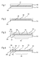
- FIG. 1 As already mentioned, a known device has a light-emitting element LE which is mounted on a substrate SU. With the aid of a sealant DM, a cover AD is arranged above the light-emitting element.
- FIG. 2 shows a further known device in which the cover AD is formed like a cap and the light-emitting element LE covers without contact.
- the sealant DM is limited here to the support area of the cover, which corresponds to the sealing area.
- a getter material GE is applied on the inside of the cover AD.
- FIG. 3 shows the proposed, in contrast, improved device in which the cover AD by means of support elements SE, which are an integral part of the cover, seated on the light-emitting element LE.
- the support elements SE are for example supported evenly on a support area AB.
- On the inside of the cover AD Getter material GE is applied between the arbitrarily shaped, shown here with conical cross-section support elements.
- the cover AD is provided with a single recess V interrupted only by the support elements SE.
- the lower edge of the cover is eg in a plane with the lower edge of the support elements SE, but can deviate therefrom, depending on how the layer thickness of the sealant is to be selected between the cover AD and the substrate SU.
- FIG. 4 shows a further embodiment of a device according to the invention, in which the cover AD centrally in a support region AB on the light-emitting element LE supported.
- the support region AB comprises the larger area proportion of the light-emitting element LE.
- a recess V is provided in the cover, which preferably surrounds the central support element SE in an annular manner.
- a getter material GE is arranged so that it does not come into contact with the light-emitting element, in particular the OLED.
- the substrate SU has an edge region RB enclosing the light-emitting element LE. Within this edge region, but at a distance from the outer edge of the light-emitting element LE, the sealing region DB is provided, in which a sealing means DM is provided between the cover AD and the substrate SU and seals the gap between the two elements forming the encapsulation. Between the central support element SE and the light-emitting element LE, a buffer layer PS is arranged which contacts both the support element SE and the light-emitting element LE.
- the depression V is provided near the sealing region or adjoins it and may be arranged completely within the edge region RD. It is also possible, however, as in the FIG. 4 illustrated that the light-emitting element LE protrudes into the recess V.
- the light emitting element LE facing away from the surface of the cover AD may be flat.
- FIG. 5 shows an embodiment in which the cover AD comprises at least one glass layer in which the recesses V are impressed. This can be done in the liquid or softened state of the glass layer, which is for example a thin glass sheet. The impressing of the depressions V can also be done by pouring a glass sheet into a suitably designed glass mold.
- the cover or the glass layer of the cover can have a uniform layer thickness.
- the structuring of the depression V can be connected simultaneously with the structuring of the support elements SE.
- FIG. 6 shows an embodiment with two further details that can be independently combined with the embodiments according to the remaining figures.
- the support element has a bearing surface which occupies the entire support region and approximately corresponds to the base of the light-emitting element LE, so that it is completely covered by the buffer layer and the support element.
- FIG. 7 shows in plan view a possible division of the bases of a light-emitting device according to the invention.
- the surfaces or boundaries are arranged concentrically, wherein the general basic shape of the light-emitting device may have any outline, but preferably is rectangular or round.
- the sealing area DB adjoins the outer edge of the cover AD.
- the edge region RB is provided, which is free of light-emitting element.
- the supporting area AB Within which either a central support element SE rests on the light-emitting element LE or within which individual distributed over the supporting area AB smaller support elements SE are distributed.
- the depression can connect to the sealing region DB on the inside and at least partially overlaps the edge region RB.
- the dashed lines outer edge of the light-emitting element LE adjoins the edge region, but may also coincide with the support region AB or its outer boundary.
Landscapes
- Physics & Mathematics (AREA)
- Optics & Photonics (AREA)
- Electroluminescent Light Sources (AREA)
- Planar Illumination Modules (AREA)
- Led Device Packages (AREA)
Applications Claiming Priority (1)
| Application Number | Priority Date | Filing Date | Title |
|---|---|---|---|
| DE102006061943.9A DE102006061943B4 (de) | 2006-12-29 | 2006-12-29 | Lichtemittierende Vorrichtung |
Publications (3)
| Publication Number | Publication Date |
|---|---|
| EP1939953A2 true EP1939953A2 (fr) | 2008-07-02 |
| EP1939953A3 EP1939953A3 (fr) | 2011-08-17 |
| EP1939953B1 EP1939953B1 (fr) | 2018-02-07 |
Family
ID=39228360
Family Applications (1)
| Application Number | Title | Priority Date | Filing Date |
|---|---|---|---|
| EP07122425.7A Active EP1939953B1 (fr) | 2006-12-29 | 2007-12-05 | Dispositif émettant de la lumière |
Country Status (4)
| Country | Link |
|---|---|
| US (1) | US8330360B2 (fr) |
| EP (1) | EP1939953B1 (fr) |
| JP (1) | JP2008166272A (fr) |
| DE (1) | DE102006061943B4 (fr) |
Cited By (1)
| Publication number | Priority date | Publication date | Assignee | Title |
|---|---|---|---|---|
| WO2010059043A1 (fr) * | 2008-11-20 | 2010-05-27 | Nederlandse Organisatie Voor Toegepast-Natuurwetenschappelijk Onderzoek Tno | Dispositif électronique et procédé de fabrication d'un dispositif électronique |
Families Citing this family (10)
| Publication number | Priority date | Publication date | Assignee | Title |
|---|---|---|---|---|
| KR101200258B1 (ko) * | 2008-12-26 | 2012-11-12 | 엘지디스플레이 주식회사 | 액정표시장치용 모 어레이 기판 |
| KR101351409B1 (ko) * | 2009-06-03 | 2014-01-14 | 엘지디스플레이 주식회사 | 유기전계발광표시장치 및 그 제조방법 |
| KR20110007654A (ko) * | 2009-07-17 | 2011-01-25 | 엘지디스플레이 주식회사 | 유기전계 발광소자 및 그 제조 방법 |
| KR101577230B1 (ko) | 2009-09-22 | 2015-12-15 | 엘지디스플레이 주식회사 | 유기 발광 표시 장치 및 이의 제조 방법 |
| EP2586077B1 (fr) | 2010-06-22 | 2016-12-14 | Koninklijke Philips N.V. | Dispositif électroluminescent organique avec feuille de séparation |
| KR101927942B1 (ko) * | 2012-02-09 | 2018-12-12 | 삼성디스플레이 주식회사 | 유기 발광 디스플레이 장치와, 이의 제조 방법 |
| KR102009725B1 (ko) * | 2012-09-06 | 2019-08-13 | 삼성디스플레이 주식회사 | 유기 발광 표시 장치 및 그 제조 방법 |
| CN104183614B (zh) * | 2013-05-24 | 2017-06-06 | 群创光电股份有限公司 | 有机发光显示装置 |
| TWI535003B (zh) * | 2013-05-24 | 2016-05-21 | 群創光電股份有限公司 | 有機發光顯示裝置 |
| KR102448843B1 (ko) | 2017-12-29 | 2022-09-28 | 엘지디스플레이 주식회사 | 유기전계발광 표시장치 및 그 제조방법 |
Family Cites Families (37)
| Publication number | Priority date | Publication date | Assignee | Title |
|---|---|---|---|---|
| JPS6132807A (ja) | 1984-07-26 | 1986-02-15 | Toshiba Corp | 光フアイバ心線固定具及びその製造方法 |
| EP0213426A1 (fr) | 1985-08-30 | 1987-03-11 | Siemens Aktiengesellschaft | Boîtier avec une partie de fond et une couverture extérieure pour un élément de circuit électrique |
| JPS62145336A (ja) | 1985-12-19 | 1987-06-29 | Mitsubishi Electric Corp | 計算機システムのプログラムル−プ検出方式 |
| DE9100665U1 (de) | 1991-01-21 | 1992-07-16 | TELBUS Gesellschaft für elektronische Kommunikations-Systeme mbH, 85391 Allershausen | Trägerelement für integrierte Halbleiter-Schaltkreise, insbesondere zum Einbau in Chip-Karten |
| US5175395A (en) | 1991-11-27 | 1992-12-29 | Rockwell International Corporation | Electromagnetic shield |
| JP2962939B2 (ja) | 1992-07-21 | 1999-10-12 | 京セラ株式会社 | 半導体素子収納用パッケージ |
| US5455456A (en) | 1993-09-15 | 1995-10-03 | Lsi Logic Corporation | Integrated circuit package lid |
| US5604978A (en) * | 1994-12-05 | 1997-02-25 | International Business Machines Corporation | Method for cooling of chips using a plurality of materials |
| JPH08274208A (ja) | 1995-03-29 | 1996-10-18 | Toyo Commun Equip Co Ltd | セラミックパッケージの封止蓋の構造 |
| US5972738A (en) | 1997-05-07 | 1999-10-26 | Lsi Logic Corporation | PBGA stiffener package |
| EP1038312A1 (fr) | 1998-01-07 | 2000-09-27 | Fed Corporation | Ensemble et procede de conditionnement de dispositifs de visualisation integree |
| JP3139462B2 (ja) | 1998-07-17 | 2001-02-26 | 日本電気株式会社 | 有機薄膜elデバイスの製造方法 |
| US7394153B2 (en) | 1999-12-17 | 2008-07-01 | Osram Opto Semiconductors Gmbh | Encapsulation of electronic devices |
| WO2001045140A2 (fr) | 1999-12-17 | 2001-06-21 | Osram Opto Semiconductors Gmbh | Encapsulation d'une del organique |
| DE10004964B4 (de) | 2000-02-04 | 2010-07-29 | Robert Bosch Gmbh | Mikromechanische Kappenstruktur |
| US6400014B1 (en) | 2001-01-13 | 2002-06-04 | Siliconware Precision Industries Co., Ltd. | Semiconductor package with a heat sink |
| US6664563B2 (en) * | 2001-03-30 | 2003-12-16 | Sanyo Electric Co., Ltd. | Electroluminescence device with shock buffer function and sealing member with shock buffer function for the same |
| JP2002319710A (ja) | 2001-04-20 | 2002-10-31 | Matsushita Electric Ind Co Ltd | 発光装置とその製造方法 |
| DE10137619A1 (de) | 2001-08-01 | 2003-02-27 | Infineon Technologies Ag | Abdeckelement für Baugruppen |
| DE10200382B4 (de) | 2002-01-08 | 2006-05-04 | Infineon Technologies Ag | Chipmodul für Chipkarten |
| KR100675625B1 (ko) * | 2002-08-08 | 2007-02-01 | 엘지.필립스 엘시디 주식회사 | 유기전계발광소자 및 그 제조방법 |
| JP2004084651A (ja) * | 2002-08-28 | 2004-03-18 | Hideaki Todoroki | 内燃機関用点火プラグゴードおよび内燃機関用ダイレクトイグニションの点火火花を強くする点火用装置とその取り付け方法 |
| US20040048033A1 (en) | 2002-09-11 | 2004-03-11 | Osram Opto Semiconductors (Malaysia) Sdn. Bhd. | Oled devices with improved encapsulation |
| US7193364B2 (en) | 2002-09-12 | 2007-03-20 | Osram Opto Semiconductors (Malaysia) Sdn. Bhd | Encapsulation for organic devices |
| JP2004227792A (ja) | 2003-01-20 | 2004-08-12 | Renesas Technology Corp | 有機エレクトロルミネッセンス表示装置 |
| US7045868B2 (en) | 2003-07-31 | 2006-05-16 | Motorola, Inc. | Wafer-level sealed microdevice having trench isolation and methods for making the same |
| JP2005166315A (ja) * | 2003-11-28 | 2005-06-23 | Toshiba Matsushita Display Technology Co Ltd | 有機el表示装置 |
| JP2005340020A (ja) * | 2004-05-27 | 2005-12-08 | Hitachi Displays Ltd | 有機エレクトロルミネッセンス表示装置およびその製造方法 |
| US7405924B2 (en) | 2004-09-27 | 2008-07-29 | Idc, Llc | System and method for protecting microelectromechanical systems array using structurally reinforced back-plate |
| US7638942B2 (en) * | 2004-10-11 | 2009-12-29 | Lg Display Co., Ltd. | Encapsulation cap having a getter and display device using the same |
| US20060093795A1 (en) * | 2004-11-04 | 2006-05-04 | Eastman Kodak Company | Polymeric substrate having a desiccant layer |
| US7329560B2 (en) | 2004-12-10 | 2008-02-12 | Osram Opto Semiconductors Gmbh | Method for encapsulating at least one organic light-emitting (OLED) device and OLED device |
| KR20060066399A (ko) * | 2004-12-13 | 2006-06-16 | 삼성전자주식회사 | 면광원 장치 및 이를 갖는 표시장치 |
| GB0505680D0 (en) | 2005-03-22 | 2005-04-27 | Cambridge Display Tech Ltd | Apparatus and method for increased device lifetime in an organic electro-luminescent device |
| WO2006101378A1 (fr) * | 2005-03-25 | 2006-09-28 | Lg Electronics Inc. | Dispositif electroluminescent |
| US7368307B2 (en) | 2005-06-07 | 2008-05-06 | Eastman Kodak Company | Method of manufacturing an OLED device with a curved light emitting surface |
| US8830695B2 (en) | 2007-01-25 | 2014-09-09 | Osram Opto Semiconductors Gmbh | Encapsulated electronic device |
-
2006
- 2006-12-29 DE DE102006061943.9A patent/DE102006061943B4/de active Active
-
2007
- 2007-12-05 EP EP07122425.7A patent/EP1939953B1/fr active Active
- 2007-12-12 JP JP2007320454A patent/JP2008166272A/ja active Pending
- 2007-12-20 US US11/961,896 patent/US8330360B2/en active Active
Non-Patent Citations (1)
| Title |
|---|
| None |
Cited By (1)
| Publication number | Priority date | Publication date | Assignee | Title |
|---|---|---|---|---|
| WO2010059043A1 (fr) * | 2008-11-20 | 2010-05-27 | Nederlandse Organisatie Voor Toegepast-Natuurwetenschappelijk Onderzoek Tno | Dispositif électronique et procédé de fabrication d'un dispositif électronique |
Also Published As
| Publication number | Publication date |
|---|---|
| DE102006061943B4 (de) | 2023-03-30 |
| DE102006061943A1 (de) | 2008-07-03 |
| US20080224601A1 (en) | 2008-09-18 |
| EP1939953A3 (fr) | 2011-08-17 |
| US8330360B2 (en) | 2012-12-11 |
| JP2008166272A (ja) | 2008-07-17 |
| EP1939953B1 (fr) | 2018-02-07 |
Similar Documents
| Publication | Publication Date | Title |
|---|---|---|
| EP1939953B1 (fr) | Dispositif émettant de la lumière | |
| DE69937407T2 (de) | Verkapselung einer vorrichtung | |
| DE60006211T2 (de) | Organische elektrolumineszente vorrichtung | |
| DE102013106855B4 (de) | Verfahren zum Herstellen eines optoelektronischen Bauelements und optoelektronisches Bauelement unter Verwendung einer flüssigen ersten Legierung | |
| EP2294642B1 (fr) | Procédé de fabrication d'un composant électronique organique | |
| WO2013000797A1 (fr) | Structure d'encapsulation pour composant optoélectronique et procédé d'encapsulation d'un composant optoélectronique | |
| EP1916723A2 (fr) | Diode luminescente organique et procédé de fabrication d'une diode luminescente organique | |
| DE102010032834A1 (de) | Optoelektronische Vorrichtung und Verfahren zu deren Herstellung | |
| WO2001018886A2 (fr) | Composants et leur production | |
| EP3017464B1 (fr) | Dispositif opto-électronique et sa méthode de fabrication | |
| US7781965B2 (en) | Glass encapsulation cap, organic electroluminescent device having the same, mother glass substrate for producing multiple glass encapsulation caps, and manufacturing method thereof | |
| DE102004049955B4 (de) | Verfahren zur Herstellung eines optischen Bauelements, insbesondere einer OLED | |
| DE102011079160B4 (de) | Verkapselungsstruktur für ein optoelektronisches bauelement und verfahren zum verkapseln eines optoelektronischen bauelements | |
| WO2014207039A1 (fr) | Composant optoélectronique et procédé de fabrication d'un composant optoélectronique | |
| DE102011076733A1 (de) | Optoelektronisches Bauelement, Verfahren zum Herstellen eines optoelektronischen Bauelements, Verwendung einer Glasfritte zur Kantenpassivierung einer Elektrode eines optoelektronischen Bauelements, und Verwendung einer Glasfritte zur Passivierung einer o | |
| DE102015103702B4 (de) | Verfahren zum Herstellen eines optoelektronischen Bauelements | |
| WO2024213747A1 (fr) | Composant électronique et procédé de production d'un composant électronique | |
| DE112015000473B4 (de) | Licht emittierendes Bauelement | |
| DE102007012504B4 (de) | Elektronische Vorrichtung | |
| DE102014110268B4 (de) | Verfahren zum Herstellen eines optoelektronischen Bauelements | |
| WO2017191194A2 (fr) | Procédé de fabrication d'un composant optoélectronique organique et composant optoélectronique organique | |
| DE102016109490A1 (de) | Verfahren zum herstellen eines organischen optoelektronischen bauelements und organisches optoelektronisches bauelement | |
| AT413170B (de) | Dünnschichtanordnung und verfahren zum herstellen einer solchen dünnschichtanordnung | |
| DE102015118417A1 (de) | Optoelektronisches Bauelement und Verfahren zum Herstellen eines optoelektronischen Bauelements | |
| WO2016042042A1 (fr) | Module optoélectronique et procédé de fabrication d'un module optoélectronique |
Legal Events
| Date | Code | Title | Description |
|---|---|---|---|
| PUAI | Public reference made under article 153(3) epc to a published international application that has entered the european phase |
Free format text: ORIGINAL CODE: 0009012 |
|
| AK | Designated contracting states |
Kind code of ref document: A2 Designated state(s): AT BE BG CH CY CZ DE DK EE ES FI FR GB GR HU IE IS IT LI LT LU LV MC MT NL PL PT RO SE SI SK TR |
|
| AX | Request for extension of the european patent |
Extension state: AL BA HR MK RS |
|
| RIN1 | Information on inventor provided before grant (corrected) |
Inventor name: FRISCHKNECHT, KYLE D. |
|
| PUAL | Search report despatched |
Free format text: ORIGINAL CODE: 0009013 |
|
| AK | Designated contracting states |
Kind code of ref document: A3 Designated state(s): AT BE BG CH CY CZ DE DK EE ES FI FR GB GR HU IE IS IT LI LT LU LV MC MT NL PL PT RO SE SI SK TR |
|
| AX | Request for extension of the european patent |
Extension state: AL BA HR MK RS |
|
| RIC1 | Information provided on ipc code assigned before grant |
Ipc: H01L 51/52 20060101AFI20110712BHEP |
|
| 17P | Request for examination filed |
Effective date: 20120111 |
|
| AKX | Designation fees paid |
Designated state(s): AT BE BG CH CY CZ DE DK EE ES FI FR GB GR HU IE IS IT LI LT LU LV MC MT NL PL PT RO SE SI SK TR |
|
| RAP1 | Party data changed (applicant data changed or rights of an application transferred) |
Owner name: OSRAM OLED GMBH |
|
| GRAP | Despatch of communication of intention to grant a patent |
Free format text: ORIGINAL CODE: EPIDOSNIGR1 |
|
| INTG | Intention to grant announced |
Effective date: 20170830 |
|
| GRAS | Grant fee paid |
Free format text: ORIGINAL CODE: EPIDOSNIGR3 |
|
| GRAA | (expected) grant |
Free format text: ORIGINAL CODE: 0009210 |
|
| AK | Designated contracting states |
Kind code of ref document: B1 Designated state(s): AT BE BG CH CY CZ DE DK EE ES FI FR GB GR HU IE IS IT LI LT LU LV MC MT NL PL PT RO SE SI SK TR |
|
| REG | Reference to a national code |
Ref country code: GB Ref legal event code: FG4D Free format text: NOT ENGLISH |
|
| REG | Reference to a national code |
Ref country code: AT Ref legal event code: REF Ref document number: 969105 Country of ref document: AT Kind code of ref document: T Effective date: 20180215 Ref country code: CH Ref legal event code: EP |
|
| REG | Reference to a national code |
Ref country code: IE Ref legal event code: FG4D Free format text: LANGUAGE OF EP DOCUMENT: GERMAN |
|
| REG | Reference to a national code |
Ref country code: DE Ref legal event code: R096 Ref document number: 502007016053 Country of ref document: DE |
|
| REG | Reference to a national code |
Ref country code: NL Ref legal event code: MP Effective date: 20180207 |
|
| PG25 | Lapsed in a contracting state [announced via postgrant information from national office to epo] |
Ref country code: FI Free format text: LAPSE BECAUSE OF FAILURE TO SUBMIT A TRANSLATION OF THE DESCRIPTION OR TO PAY THE FEE WITHIN THE PRESCRIBED TIME-LIMIT Effective date: 20180207 Ref country code: ES Free format text: LAPSE BECAUSE OF FAILURE TO SUBMIT A TRANSLATION OF THE DESCRIPTION OR TO PAY THE FEE WITHIN THE PRESCRIBED TIME-LIMIT Effective date: 20180207 Ref country code: CY Free format text: LAPSE BECAUSE OF FAILURE TO SUBMIT A TRANSLATION OF THE DESCRIPTION OR TO PAY THE FEE WITHIN THE PRESCRIBED TIME-LIMIT Effective date: 20180207 Ref country code: LT Free format text: LAPSE BECAUSE OF FAILURE TO SUBMIT A TRANSLATION OF THE DESCRIPTION OR TO PAY THE FEE WITHIN THE PRESCRIBED TIME-LIMIT Effective date: 20180207 Ref country code: NL Free format text: LAPSE BECAUSE OF FAILURE TO SUBMIT A TRANSLATION OF THE DESCRIPTION OR TO PAY THE FEE WITHIN THE PRESCRIBED TIME-LIMIT Effective date: 20180207 |
|
| PG25 | Lapsed in a contracting state [announced via postgrant information from national office to epo] |
Ref country code: GR Free format text: LAPSE BECAUSE OF FAILURE TO SUBMIT A TRANSLATION OF THE DESCRIPTION OR TO PAY THE FEE WITHIN THE PRESCRIBED TIME-LIMIT Effective date: 20180508 Ref country code: BG Free format text: LAPSE BECAUSE OF FAILURE TO SUBMIT A TRANSLATION OF THE DESCRIPTION OR TO PAY THE FEE WITHIN THE PRESCRIBED TIME-LIMIT Effective date: 20180507 Ref country code: IS Free format text: LAPSE BECAUSE OF FAILURE TO SUBMIT A TRANSLATION OF THE DESCRIPTION OR TO PAY THE FEE WITHIN THE PRESCRIBED TIME-LIMIT Effective date: 20180607 Ref country code: PL Free format text: LAPSE BECAUSE OF FAILURE TO SUBMIT A TRANSLATION OF THE DESCRIPTION OR TO PAY THE FEE WITHIN THE PRESCRIBED TIME-LIMIT Effective date: 20180207 Ref country code: SE Free format text: LAPSE BECAUSE OF FAILURE TO SUBMIT A TRANSLATION OF THE DESCRIPTION OR TO PAY THE FEE WITHIN THE PRESCRIBED TIME-LIMIT Effective date: 20180207 Ref country code: LV Free format text: LAPSE BECAUSE OF FAILURE TO SUBMIT A TRANSLATION OF THE DESCRIPTION OR TO PAY THE FEE WITHIN THE PRESCRIBED TIME-LIMIT Effective date: 20180207 |
|
| PG25 | Lapsed in a contracting state [announced via postgrant information from national office to epo] |
Ref country code: MT Free format text: LAPSE BECAUSE OF FAILURE TO SUBMIT A TRANSLATION OF THE DESCRIPTION OR TO PAY THE FEE WITHIN THE PRESCRIBED TIME-LIMIT Effective date: 20180207 |
|
| PG25 | Lapsed in a contracting state [announced via postgrant information from national office to epo] |
Ref country code: EE Free format text: LAPSE BECAUSE OF FAILURE TO SUBMIT A TRANSLATION OF THE DESCRIPTION OR TO PAY THE FEE WITHIN THE PRESCRIBED TIME-LIMIT Effective date: 20180207 Ref country code: IT Free format text: LAPSE BECAUSE OF FAILURE TO SUBMIT A TRANSLATION OF THE DESCRIPTION OR TO PAY THE FEE WITHIN THE PRESCRIBED TIME-LIMIT Effective date: 20180207 Ref country code: RO Free format text: LAPSE BECAUSE OF FAILURE TO SUBMIT A TRANSLATION OF THE DESCRIPTION OR TO PAY THE FEE WITHIN THE PRESCRIBED TIME-LIMIT Effective date: 20180207 |
|
| REG | Reference to a national code |
Ref country code: DE Ref legal event code: R097 Ref document number: 502007016053 Country of ref document: DE |
|
| PG25 | Lapsed in a contracting state [announced via postgrant information from national office to epo] |
Ref country code: CZ Free format text: LAPSE BECAUSE OF FAILURE TO SUBMIT A TRANSLATION OF THE DESCRIPTION OR TO PAY THE FEE WITHIN THE PRESCRIBED TIME-LIMIT Effective date: 20180207 Ref country code: SK Free format text: LAPSE BECAUSE OF FAILURE TO SUBMIT A TRANSLATION OF THE DESCRIPTION OR TO PAY THE FEE WITHIN THE PRESCRIBED TIME-LIMIT Effective date: 20180207 Ref country code: DK Free format text: LAPSE BECAUSE OF FAILURE TO SUBMIT A TRANSLATION OF THE DESCRIPTION OR TO PAY THE FEE WITHIN THE PRESCRIBED TIME-LIMIT Effective date: 20180207 |
|
| PLBE | No opposition filed within time limit |
Free format text: ORIGINAL CODE: 0009261 |
|
| STAA | Information on the status of an ep patent application or granted ep patent |
Free format text: STATUS: NO OPPOSITION FILED WITHIN TIME LIMIT |
|
| 26N | No opposition filed |
Effective date: 20181108 |
|
| PG25 | Lapsed in a contracting state [announced via postgrant information from national office to epo] |
Ref country code: SI Free format text: LAPSE BECAUSE OF FAILURE TO SUBMIT A TRANSLATION OF THE DESCRIPTION OR TO PAY THE FEE WITHIN THE PRESCRIBED TIME-LIMIT Effective date: 20180207 |
|
| REG | Reference to a national code |
Ref country code: CH Ref legal event code: PL |
|
| GBPC | Gb: european patent ceased through non-payment of renewal fee |
Effective date: 20181205 |
|
| PG25 | Lapsed in a contracting state [announced via postgrant information from national office to epo] |
Ref country code: MC Free format text: LAPSE BECAUSE OF FAILURE TO SUBMIT A TRANSLATION OF THE DESCRIPTION OR TO PAY THE FEE WITHIN THE PRESCRIBED TIME-LIMIT Effective date: 20180207 Ref country code: LU Free format text: LAPSE BECAUSE OF NON-PAYMENT OF DUE FEES Effective date: 20181205 |
|
| REG | Reference to a national code |
Ref country code: IE Ref legal event code: MM4A |
|
| REG | Reference to a national code |
Ref country code: BE Ref legal event code: MM Effective date: 20181231 |
|
| PG25 | Lapsed in a contracting state [announced via postgrant information from national office to epo] |
Ref country code: FR Free format text: LAPSE BECAUSE OF NON-PAYMENT OF DUE FEES Effective date: 20181231 Ref country code: IE Free format text: LAPSE BECAUSE OF NON-PAYMENT OF DUE FEES Effective date: 20181205 |
|
| PG25 | Lapsed in a contracting state [announced via postgrant information from national office to epo] |
Ref country code: BE Free format text: LAPSE BECAUSE OF NON-PAYMENT OF DUE FEES Effective date: 20181231 |
|
| PG25 | Lapsed in a contracting state [announced via postgrant information from national office to epo] |
Ref country code: LI Free format text: LAPSE BECAUSE OF NON-PAYMENT OF DUE FEES Effective date: 20181231 Ref country code: CH Free format text: LAPSE BECAUSE OF NON-PAYMENT OF DUE FEES Effective date: 20181231 Ref country code: GB Free format text: LAPSE BECAUSE OF NON-PAYMENT OF DUE FEES Effective date: 20181205 |
|
| REG | Reference to a national code |
Ref country code: AT Ref legal event code: MM01 Ref document number: 969105 Country of ref document: AT Kind code of ref document: T Effective date: 20181205 |
|
| PG25 | Lapsed in a contracting state [announced via postgrant information from national office to epo] |
Ref country code: TR Free format text: LAPSE BECAUSE OF FAILURE TO SUBMIT A TRANSLATION OF THE DESCRIPTION OR TO PAY THE FEE WITHIN THE PRESCRIBED TIME-LIMIT Effective date: 20180207 |
|
| PG25 | Lapsed in a contracting state [announced via postgrant information from national office to epo] |
Ref country code: AT Free format text: LAPSE BECAUSE OF NON-PAYMENT OF DUE FEES Effective date: 20181205 |
|
| PG25 | Lapsed in a contracting state [announced via postgrant information from national office to epo] |
Ref country code: PT Free format text: LAPSE BECAUSE OF FAILURE TO SUBMIT A TRANSLATION OF THE DESCRIPTION OR TO PAY THE FEE WITHIN THE PRESCRIBED TIME-LIMIT Effective date: 20180207 |
|
| PG25 | Lapsed in a contracting state [announced via postgrant information from national office to epo] |
Ref country code: HU Free format text: LAPSE BECAUSE OF FAILURE TO SUBMIT A TRANSLATION OF THE DESCRIPTION OR TO PAY THE FEE WITHIN THE PRESCRIBED TIME-LIMIT; INVALID AB INITIO Effective date: 20071205 |
|
| REG | Reference to a national code |
Ref country code: DE Ref legal event code: R081 Ref document number: 502007016053 Country of ref document: DE Owner name: PICTIVA DISPLAYS INTERNATIONAL LIMITED, IE Free format text: FORMER OWNER: OSRAM OLED GMBH, 93049 REGENSBURG, DE Ref country code: DE Ref legal event code: R082 Ref document number: 502007016053 Country of ref document: DE Representative=s name: EPPING HERMANN FISCHER PATENTANWALTSGESELLSCHA, DE |
|
| REG | Reference to a national code |
Ref country code: DE Ref legal event code: R079 Ref document number: 502007016053 Country of ref document: DE Free format text: PREVIOUS MAIN CLASS: H01L0051520000 Ipc: H10K0050800000 |
|
| PGFP | Annual fee paid to national office [announced via postgrant information from national office to epo] |
Ref country code: DE Payment date: 20251216 Year of fee payment: 19 |