EP1939982A1 - Substrat à impédance élevée, dispositif d'antenne et dispositif radio mobile - Google Patents
Substrat à impédance élevée, dispositif d'antenne et dispositif radio mobile Download PDFInfo
- Publication number
- EP1939982A1 EP1939982A1 EP07254747A EP07254747A EP1939982A1 EP 1939982 A1 EP1939982 A1 EP 1939982A1 EP 07254747 A EP07254747 A EP 07254747A EP 07254747 A EP07254747 A EP 07254747A EP 1939982 A1 EP1939982 A1 EP 1939982A1
- Authority
- EP
- European Patent Office
- Prior art keywords
- metal plates
- ground plane
- finite ground
- impedance
- conductive elements
- Prior art date
- Legal status (The legal status is an assumption and is not a legal conclusion. Google has not performed a legal analysis and makes no representation as to the accuracy of the status listed.)
- Withdrawn
Links
- 239000000758 substrate Substances 0.000 title claims abstract description 129
- 239000002184 metal Substances 0.000 claims abstract description 170
- 239000011159 matrix material Substances 0.000 claims abstract description 13
- 230000005404 monopole Effects 0.000 claims description 7
- 238000010586 diagram Methods 0.000 description 53
- 239000004020 conductor Substances 0.000 description 28
- 238000005530 etching Methods 0.000 description 7
- 238000000034 method Methods 0.000 description 5
- 230000000694 effects Effects 0.000 description 4
- 238000004519 manufacturing process Methods 0.000 description 4
- 230000037361 pathway Effects 0.000 description 2
- 238000007747 plating Methods 0.000 description 2
- 230000005855 radiation Effects 0.000 description 2
- 230000009467 reduction Effects 0.000 description 2
- 230000015572 biosynthetic process Effects 0.000 description 1
- 230000008859 change Effects 0.000 description 1
- 230000006866 deterioration Effects 0.000 description 1
- 239000000284 extract Substances 0.000 description 1
- 230000014509 gene expression Effects 0.000 description 1
- 238000007689 inspection Methods 0.000 description 1
- 230000002093 peripheral effect Effects 0.000 description 1
- 230000008569 process Effects 0.000 description 1
Images



Classifications
-
- H—ELECTRICITY
- H01—ELECTRIC ELEMENTS
- H01Q—ANTENNAS, i.e. RADIO AERIALS
- H01Q15/00—Devices for reflection, refraction, diffraction or polarisation of waves radiated from an antenna, e.g. quasi-optical devices
- H01Q15/0006—Devices acting selectively as reflecting surface, as diffracting or as refracting device, e.g. frequency filtering or angular spatial filtering devices
- H01Q15/006—Selective devices having photonic band gap materials or materials of which the material properties are frequency dependent, e.g. perforated substrates, high-impedance surfaces
- H01Q15/0066—Selective devices having photonic band gap materials or materials of which the material properties are frequency dependent, e.g. perforated substrates, high-impedance surfaces said selective devices being reconfigurable, tunable or controllable, e.g. using switches
-
- H—ELECTRICITY
- H05—ELECTRIC TECHNIQUES NOT OTHERWISE PROVIDED FOR
- H05K—PRINTED CIRCUITS; CASINGS OR CONSTRUCTIONAL DETAILS OF ELECTRIC APPARATUS; MANUFACTURE OF ASSEMBLAGES OF ELECTRICAL COMPONENTS
- H05K1/00—Printed circuits
- H05K1/02—Details
-
- H—ELECTRICITY
- H01—ELECTRIC ELEMENTS
- H01Q—ANTENNAS, i.e. RADIO AERIALS
- H01Q1/00—Details of, or arrangements associated with, antennas
- H01Q1/12—Supports; Mounting means
- H01Q1/22—Supports; Mounting means by structural association with other equipment or articles
- H01Q1/24—Supports; Mounting means by structural association with other equipment or articles with receiving set
- H01Q1/241—Supports; Mounting means by structural association with other equipment or articles with receiving set used in mobile communications, e.g. GSM
- H01Q1/242—Supports; Mounting means by structural association with other equipment or articles with receiving set used in mobile communications, e.g. GSM specially adapted for hand-held use
- H01Q1/243—Supports; Mounting means by structural association with other equipment or articles with receiving set used in mobile communications, e.g. GSM specially adapted for hand-held use with built-in antennas
-
- H—ELECTRICITY
- H01—ELECTRIC ELEMENTS
- H01Q—ANTENNAS, i.e. RADIO AERIALS
- H01Q15/00—Devices for reflection, refraction, diffraction or polarisation of waves radiated from an antenna, e.g. quasi-optical devices
- H01Q15/0006—Devices acting selectively as reflecting surface, as diffracting or as refracting device, e.g. frequency filtering or angular spatial filtering devices
- H01Q15/006—Selective devices having photonic band gap materials or materials of which the material properties are frequency dependent, e.g. perforated substrates, high-impedance surfaces
- H01Q15/008—Selective devices having photonic band gap materials or materials of which the material properties are frequency dependent, e.g. perforated substrates, high-impedance surfaces said selective devices having Sievenpipers' mushroom elements
Definitions
- the present invention relates to a high-impedance substrate, an antenna device and a mobile radio device, and relates to, for example, a technique for downsizing high-impedance substrates.
- a conventional high-impedance substrate has a structure in which a large number of metal patches (metal plates) are periodically arranged.
- One conventional issue that can be surmounted by such a high-impedance substrate is the adoption of a low profile for an antenna on a conductor plate.
- National Publication of International Patent Application No. 2004-535720 utilizes its advantages to achieve a low-profile antenna on the rooftop of an automobile, thereby solving the conventional problems existing in vehicle-mounted antennas with respect to mechanical strength and aesthetic properties.
- mounting on a small-sized device is difficult.
- mounting a conventional high-impedance substrate on extremely small devices such as a mobile phone is difficult even if the substrate includes only two rows of metal patches.
- a conventional high-impedance substrate has a problem in that mounting on a small-sized device is difficult.
- a high-impedance substrate comprising:
- an antenna device comprising the high-impedance substrate according to the first aspect of the present invention and a monopole antenna or a dipole antenna at the predetermined height from the finite ground plane or at a higher height.
- a portable radio device comprising:
- a high-impedance substrate comprising:
- a high-impedance substrate comprising:
- FIG. 1 is a perspective view showing a configuration of a high-impedance substrate according to a first embodiment of the present invention.
- This high-impedance substrate includes a finite ground plane 1, rectangular metal patches (metal plates) 2 periodically-arranged in two rows (arranged in a 2-row, 5-column matrix pattern) on the finite ground plane 1, and linear conductors (linear conductive elements) 3 that short-circuit the finite ground plane 1 and the metal patches 2.
- the finite ground plane 1 is made of conducting material. Since the essence of the realization of a high-impedance substrate lies in the arrangement of the metal patches 2, the area of the finite ground plane 1 is nonessential. Therefore, while FIG. 1 shows the area of the finite ground plane 1 to be equivalent to the area over which the metal patches are arranged in order to attain maximum downsizing of the overall configuration, the area of the finite ground plane 1 may just as well be greater than the arrangement area.
- the metal patches 2 are made of conducting material having a rectangular planar shape.
- the two rows of metal patches are respectively periodically-arranged, and a high-impedance substrate can be realized at an arbitrary frequency band by varying the distance of the metal patches from the finite ground plane, the spacing between the metal patches, the area of a metal patch or the like.
- the distance from the finite ground plane need only be shorter than 1/4 wavelength of the frequency, and the spacing between the metal patches, the area of a metal patch and the like need only be determined so as to satisfy known relational expressions.
- the plane of the metal patches 2 is approximately parallel to the plane of the finite ground plane 1.
- the metal patches on both ends of each column are configured to be half as long in the column-wise direction.
- FIG. 1 While an example having a total of 10 metal patches in 2 rows by 5 columns is shown in FIG. 1 , the numbers of rows and columns are not limited to this example and may instead be increased or reduced according to implementation conditions. In particular, forming a matrix of four (2 rows by 2 columns) metal patches is certainly acceptable.
- the linear conductors 3 are made of conducting material, and short-circuit the above-described finite ground plane 1 and the metal patches 2.
- the linear conductors 3 are connected at edges of the metal patches 2. More specifically, metal patches (first metal patches) 2 arranged at corners (intersections of columns and rows) are connected with linear conductors 3 at intersections of sides on which an adjacent metal patch does not exist, while metal patches (second metal patches) 2 arranged at portions other than a corner (an intersection of a column and a row) are connected with linear conductors 3 at the center of a side on which an adjacent metal patch does not exist.
- the above configuration provides the high-impedance substrate shown in FIG. 1 with high-impedance characteristics. A principle of operation of this high-impedance substrate will now be described.
- FIG. 10 is a schematic diagram of a high-impedance substrate shown in FIG. 1 seen from a direction parallel to the finite ground plane 1.
- This diagram extracts metal patches 2 and linear conductors 3 corresponding to one period.
- electrical charges tend to accumulate in a proximity of two adjacent metal patches 2 due to a high-frequency current.
- This proximity can be considered to be an equivalent circuit of a capacitance C.
- a phase-change occurs on a pathway passing through the finite ground plane 1 that is opposite to the capacitance C. Therefore, this pathway can be considered to be an equivalent circuit of an inductance L. Accordingly, since the entire structure shown in FIG.
- the left diagram in FIG. 11 shows a 1-period (2-row), 1-period (2-column) high-impedance substrate seen from a side that is perpendicular to the finite ground plane 1 and which includes the metal patches 2.
- the four metal patches 2 have quadrature planar shapes and are short-circuited at centers thereof by linear conductors 3 to the finite ground plane 1. Since the structure is rotationally symmetric, high-impedance characteristics can be achieved at the same frequency hand with respect to high-frequency currents in both the directions "X" and "Y" depicted in the diagram. In this state, as shown in the center diagram, the respective metal patches 2 are bisected at planes passing through the linear conductors 3.
- the structure shown in the center diagram is capable of performing exactly the same operations as those performed by the structure shown in the left diagram.
- a portion 20 shown in the center diagram, which is now considered to be one period, is extracted and shown in the right diagram. Since one period in the "X" direction was extracted, the high-impedance characteristics in the "Y" direction are the same as that of the center diagram.
- the right diagram has high-impedance characteristics in the "X” direction as well. From the foregoing description, it is apparent that the left and right diagrams have high-impedance characteristics at the same frequency band.
- the left diagram in FIG. 12 is the same as the right diagram in FIG. 11 .
- the metal patches can be cut in the "Y" direction as shown in the center diagram.
- the configuration shown in the center diagram performs the same operation as those of the left diagram with respect to high frequencies.
- a portion 21 shown in the center diagram which is now considered to be one period in the "Y" direction, is extracted and shown in the right diagram. Since one period in the "Y" direction was extracted, the high-impedance characteristics in the "X" direction are exactly the same as those of the center diagram.
- the high-impedance substrate shown in the right diagram exhibits high-impedance characteristics in exactly the same frequency band as that of the left diagram.
- the high-impedance substrate shown in the left diagram in FIG. 11 and the high-impedance substrate shown in the right diagram in FIG. 12 achieve approximately the same high-impedance characteristics at the same frequency band regardless of the fact that the area has been reduced to 1/4.
- FIG. 13 An example in which the operations of FIGS. 11 and 12 are performed on a high-impedance substrate in the case of 4 periods (5 rows) by 3 periods (4 columns) is shown in FIG. 13 .
- downsizing of the high-impedance substrate may be performed as shown in the right diagram. While the effects of downsizing are sacrificed by the cutoff position (the dotted line in the left diagram) when performing the operations of FIGS. 11 and 12 , the position may be expanded outwards in the directions 41.
- the areas of the metal patches arranged at the outermost periphery are smaller than the planar areas of the metal patches arranged inside the metal patches arranged at the outermost periphery.
- the outer metal patches arranged at the outermost periphery are connected with linear conductors at their edges (outer peripheral portions).
- metal patches (first metal patches) 31 that are arranged at corners (intersections of lateral (row-wise) metal patch rows and longitudinal (column-wise) metal patch columns) are connected with linear conductors at intersections 32 of sides on which an adjacent metal patch does not exist, while metal patches (second metal patches) 33 other than the metal patches 31 among the outer metal patches are connected with linear conductors at the center of a side 34 on which an adjacent metal patch does not exist. While the metal patches arranged inside the outer metal patches are connected with linear conductors at their center portions, these positions may be altered according to desired impedance characteristics.
- a conventional M-row, N-column high-impedance where "M” and “N” are integers equal to or greater than 2, may be downsized by the present embodiment to an area of (M-1) by (N-1). Moreover, the characteristics as a high-impedance substrate hardly change, if at all.
- FIG. 2 is a configuration diagram of a high-impedance substrate according to a second embodiment of the present invention.
- This high-impedance substrate is configured such that a dielectric substrate 4 is provided on the finite ground plane 1 of the high-impedance substrate shown in FIG. 1 .
- the finite ground plane 1 comes into contact with one face (rear face) of the dielectric substrate 4, and metal patches 2 are arranged in a matrix pattern on the face of the dielectric substrate 4 opposite to the finite ground plane 1 (front face).
- Linear conductors 3 that short-circuit the metal patches 2 and the finite ground plane 1 are formed on the side faces (lateral faces) of the dielectric substrate 4.
- metal patches are arranged in a 2 by 5 matrix pattern, for arrangements having a larger number of metal patches such as 5 by 5, linear conductors connected with the metal patches inside the outer metal patches of the outermost periphery penetrate the interior of the dielectric substrate 4 and come into contact with the finite ground plane 1.
- the present structure can be entirely implemented by etching and metal plating or wire bonding on a so-called dielectric substrate frequently used in circuit implementation and the like.
- both the structures of the finite ground plane 1 and the metal patches 2 may be formed by performing etching on a double-sided blank PCB in which two faces (front and rear faces) of the dielectric substrate 4 are covered with metal.
- the linear conductors 3 may be produced by wire bonding in which a metal wire is stretched across the lateral face of the dielectric substrate 4 and the metal wire is soldered to the finite ground plane 1 and the metal patches 2 or by metal-plating the lateral face of the dielectric substrate 4.
- the linear conductors 3 may be manufactured by etching a metal-covered lateral face of the dielectric substrate to form striplines. In other words, providing short circuit lines on the edge (lateral face) of the dielectric substrate 4 eliminates the need for a conventional through-hole process, and enables manufacturing using basic face printing techniques. As a result, manufacturing becomes easier.
- the entire structure can now be supported by the dielectric substrate 4, and downsizing can be achieved due to the permittivity of the dielectric substrate 4.
- manufacturing can be performed using basic substrate processing techniques such as etching, cost reduction can be achieved.
- product inspection can be carried out in an easy manner.
- a high-impedance substrate of an arbitrary size may be easily manufactured by combining a plurality of 2 by 2 high-impedance substrates (refer to the right diagram in FIG. 12 ) to which the present embodiment has been applied and which have dielectric substrates. For example, arranging four 2 by 2 high-impedance substrates having dielectric substrates in a column-wise direction results in the high-impedance substrate shown in FIG. 2 . A detailed description thereof will now be provided.
- One side of a metal patch is, for example, several tens of millimeters, and the spacing between metal patches is, for example, a fraction of a millimeter.
- the spacing between metal patches is, for example, a fraction of a millimeter.
- a high-impedance substrate provided with short circuit lines at the center of the metal patches (refer to the left diagram in FIG. 11 or the left diagram in FIG. 13 )
- there is a need to manufacture a large high-impedance substrate by arranging a plurality of metal patches at spacing of a fraction of a millimeter.
- arranging metal patches at spacing of a fraction of a millimeter is difficult, and the smallest of errors (few tenths of a millimeter) may have a significant impact on performance.
- a larger high-impedance substrates can be easily manufactured.
- a side of a metal patch has a length of several tens of millimeters as described above, a small error (few tenths of a millimeter) has hardly any impact on performance.
- a 2 by 2 high-impedance substrate can be easily manufactured by etching or the like.
- a high-impedance substrate of an arbitrary size may be easily manufactured by liberally combining 2 by 2 high-impedance substrates. Consequently, the size of a high-impedance substrate can be easily changed according to the size of a chassis on which an antenna or an antenna device is to be installed. While an example has been described in which 2 by 2 high-impedance substrates to which the present embodiment has been applied and which have dielectric substrates are combined, a high-impedance substrate of an arbitrary size may be easily manufactured for the same reasons as described above by liberally combining 2 by 2 high-impedance substrates to which the present embodiment has been applied which do not have dielectric substrates.
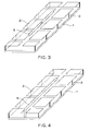
- FIG. 3 is a configuration diagram of an antenna device according to a third embodiment of the present invention.
- a dipole antenna 5 has been provided on the high-impedance substrate shown in FIG. 1 at a height that is equal to or higher than the metal patches.
- the dipole antenna 5 is arranged straight in the longitudinal direction of the high-impedance substrate, and is arranged at the center of the gap between rows of metal patches.
- the configuration Since the structure other than the dipole antenna is the same as the high-impedance substrate according to the first embodiment, the configuration has high-impedance characteristics at a specific frequency band. At this frequency, it is unlikely that a high-frequency current will flow in a direction parallel to the finite ground plane 1. Conversely, in the case where there are no metal patches and only the finite ground plane 1 exists, current flows freely over the finite ground plane 1 and a state is attained which is the same as a state where a so-called image current is assumed in a free space. Since this image current cancels the current flowing through the dipole antenna 5 and impedes the radiation of electromagnetic waves, in the case of an antenna device without metal patches, it is necessary to position the dipole antenna 5 away from the finite ground plane 1.
- the antenna device although a current is actually generated on the finite ground plane 1 so as to be equivalent to the image current, the image current is suppressed in frequency bands in which current hardly flows through the high-impedance substrate. As a result, radiation of electromagnetic waves may be obtained even when bringing the dipole antenna 5 close to the high-impedance substrate. Therefore, a low profile can be adopted for the dipole antenna 5.
- FIG. 4 is a configuration diagram of an antenna device according to a fourth embodiment of the present invention.
- a monopole antenna 6 has been provided on the high-impedance substrate shown in FIG. 1 at a height that is equal to or higher than the metal patches.
- a low profile can be adopted for the monopole antenna 6 for the same reasons as in the third embodiment.
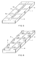
- FIG. 5 is a configuration diagram of an antenna device according to a fifth embodiment of the present invention.
- a dipole antenna 5c has been provided on the front face of the dielectric substrate 4 in the high-impedance substrate shown in FIG. 2 .
- the dipole antenna 5c is arranged straight in the longitudinal direction of the high-impedance substrate, and is arranged at the center of the gap between rows of metal patches.
- the dipole antenna 5c may be formed as a stripline on the dielectric substrate by etching.
- the entire structure including the antenna and the high-impedance substrate can now be produced using basic substrate processing techniques such as etching, thereby achieving cost reduction.
- FIG. 9 is an enlarged view of the vicinity of the feeding point 15 shown in FIG. 5 .
- a hole 7 is formed on the dielectric substrate 4 in the vicinity of the feeding point.
- Feeding is performed via a coaxial line 8 from the rear face of the finite ground plane 1.
- the coaxial line 8 penetrates the interior of the dielectric substrate 4.
- the outer conductor of the coaxial line 8 short-circuits one stripline 5c(1) of the dipole antenna 5c, while the inner conductor short-circuits the other stripline 5c(2). Since the thickness of the coaxial line 8 is generally extremely small compared to a wavelength, deterioration of characteristics of the high-impedance substrate due to the formation of the hole 7 is virtually nonexistent.
- FIG. 6 is a configuration diagram of a high-impedance substrate according to a sixth embodiment of the present invention.
- variable reactance elements 9 have been provided between adjacent metal patches 2 and at contacts between the metal patches 2 and the linear conductors 3 in the high-impedance substrate shown in FIG. 2 .
- Reactance elements may be used in place of the variable reactance elements 9.
- variable reactance elements 9 Since all of the components other than the variable reactance elements 9 are the same as those of the second embodiment, a description thereof will be omitted.
- a variable reactance element 9 is a high-frequency component capable of varying the reactance value between terminals thereof.
- a conductor such as a variable capacitance diode, a combination of a switch and a fixed reactance element, or a MEMS (MicroElectroMagnetic Systems) element may be used.
- the frequency band at which high-frequency characteristics are attained can be varied.
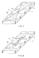
- FIG. 7 is a configuration diagram of an antenna device according to a seventh embodiment of the present invention.
- a bowtie dipole antenna 5a has been provided on the high-impedance substrate shown in FIG. 1 at a height that is slightly higher than the metal patches 2.
- the bowtie dipole antenna 5a is arranged so as to extend in the longitudinal direction of the high-impedance substrate, and is arranged at the center of the gap between rows of metal patches.
- the bowtie dipole antenna 5a is constituted by a conductor plate and has a shape that widens as the distance from the feeding point 15 increases, and is an antenna having a wider band than the dipole antenna 5. According to the configuration described above, the bowtie dipole antenna 5a achieves adoption of a low profile in the same manner as the dipole antenna according to the third embodiment. This is because, as described with respect to the first embodiment, since the high-impedance substrate has high-impedance characteristics in the longitudinal direction of the antenna as well as in a direction perpendicular thereto, currents do not flow even if the bowtie dipole antenna 5a attempts to do so in various directions on the finite ground plane 1.
- FIG. 8 is a configuration diagram of an antenna device according to an eighth embodiment of the present invention.
- a meander dipole antenna 5b has been provided on the high-impedance substrate shown in FIG. 1 at a height that is slightly higher than the metal patches 2.
- the meander dipole antenna 5b is arranged so as to extend in the longitudinal direction of the high-impedance substrate, and is arranged at the center of the gap between rows of metal patches.
- the meander dipole antenna 5b is constituted by a meander-shape linear conductor, and is an antenna whose longitudinal length is shorter than that of the dipole antenna 5c shown in FIG. 5 .
- the meander dipole antenna 5b achieves adoption of a low profile in the same manner as the dipole antenna according to the third embodiment. This is because, as described with respect to the first embodiment, since the high-impedance substrate has high-impedance characteristics in the longitudinal direction of the antenna as well as in a direction perpendicular thereto, currents do not flow even if the meander dipole antenna 5b attempts to do so in various directions on the finite ground plane 1.
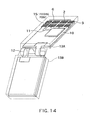
- FIG. 14 is a configuration diagram of a mobile radio device (mobile phone) according to a ninth embodiment of the present invention.
- Two chassis 13A and 13B are coupled so as to be openable and closable by a hinge cable 12.
- a high-impedance substrate on which a monopole antenna 6 is mounted (refer to FIG. 4 ); a radio circuit 10 that generates a high-frequency current; and a feeding line 11 that supplies the high-frequency current generated by the radio circuit 10 to a feeding point 15 of the monopole antenna 6.
- the radio circuit 10 is arranged on a finite ground plane of the high-impedance substrate, a plate on which the radio circuit 10 is mounted may differ from the plate of the high-impedance substrate. Since this high-impedance substrate is downsized, mounting on the radio device can be easily performed.
- FIG. 14 While an example using a high-impedance substrate on which a monopole antenna is mounted has been shown in FIG. 14 , it is obvious that a high-impedance substrate mounted with other antennas such as a dipole antenna, a meander antenna or a bowtie antenna may also be used.
- a high-impedance substrate mounted with other antennas such as a dipole antenna, a meander antenna or a bowtie antenna may also be used.
Landscapes
- Physics & Mathematics (AREA)
- Optics & Photonics (AREA)
- Engineering & Computer Science (AREA)
- Computer Networks & Wireless Communication (AREA)
- Microelectronics & Electronic Packaging (AREA)
- Details Of Aerials (AREA)
- Aerials With Secondary Devices (AREA)
Applications Claiming Priority (1)
| Application Number | Priority Date | Filing Date | Title |
|---|---|---|---|
| JP2006348380A JP2008160589A (ja) | 2006-12-25 | 2006-12-25 | 高インピーダンス基板、アンテナ装置および携帯無線装置 |
Publications (1)
| Publication Number | Publication Date |
|---|---|
| EP1939982A1 true EP1939982A1 (fr) | 2008-07-02 |
Family
ID=39203119
Family Applications (1)
| Application Number | Title | Priority Date | Filing Date |
|---|---|---|---|
| EP07254747A Withdrawn EP1939982A1 (fr) | 2006-12-25 | 2007-12-07 | Substrat à impédance élevée, dispositif d'antenne et dispositif radio mobile |
Country Status (5)
| Country | Link |
|---|---|
| US (1) | US7623087B2 (fr) |
| EP (1) | EP1939982A1 (fr) |
| JP (1) | JP2008160589A (fr) |
| KR (1) | KR20080059520A (fr) |
| CN (1) | CN101212083A (fr) |
Cited By (2)
| Publication number | Priority date | Publication date | Assignee | Title |
|---|---|---|---|---|
| EP2026411A1 (fr) * | 2007-08-09 | 2009-02-18 | Kabushiki Kaisha Toshiba | Appareil d'antenne |
| GB2495093A (en) * | 2011-09-27 | 2013-04-03 | Johan Lucas Gertenbach | Dipole antenna with a composite right and left handed transmission line |
Families Citing this family (32)
| Publication number | Priority date | Publication date | Assignee | Title |
|---|---|---|---|---|
| JPH1027581A (ja) * | 1996-07-10 | 1998-01-27 | Sakurai Yumiko | 耐圧性外囲器とその製造方法並びに前記外囲器を使用したランプ |
| US7779898B2 (en) * | 2006-04-14 | 2010-08-24 | Baltimore Aircoil Company, Inc. | Heat transfer tube assembly with serpentine circuits |
| TWI343672B (en) * | 2007-11-15 | 2011-06-11 | Lite On Technology Corp | Antenna device and antenna system utilizing which |
| JP2009135797A (ja) * | 2007-11-30 | 2009-06-18 | Toshiba Corp | アンテナ装置 |
| JP4926099B2 (ja) * | 2008-03-17 | 2012-05-09 | 三菱電機株式会社 | 電磁波反射面 |
| JP4962407B2 (ja) * | 2008-05-14 | 2012-06-27 | 株式会社デンソー | アンテナ |
| JP5214335B2 (ja) | 2008-05-30 | 2013-06-19 | 株式会社東芝 | アンテナ装置 |
| JP5112204B2 (ja) * | 2008-07-15 | 2013-01-09 | 原田工業株式会社 | アンテナエレメント間の相互結合を抑制可能なアンテナ装置 |
| JP5135178B2 (ja) | 2008-11-25 | 2013-01-30 | 株式会社東芝 | アンテナ装置および無線通信装置 |
| JP5336874B2 (ja) * | 2009-02-09 | 2013-11-06 | Necトーキン株式会社 | アンテナ装置及びrfidタグ |
| JP5276463B2 (ja) * | 2009-02-09 | 2013-08-28 | Necトーキン株式会社 | アンテナ装置及びそれを備えたrfidタグ |
| KR101038234B1 (ko) * | 2009-02-24 | 2011-06-01 | 삼성전기주식회사 | 전자기 밴드갭 구조를 이용한 emi 노이즈 저감 기판 |
| JP5398426B2 (ja) * | 2009-08-31 | 2014-01-29 | 三菱電機株式会社 | 磁気壁基板および磁気壁基板を用いたアンテナシステム |
| JP5812462B2 (ja) * | 2011-03-17 | 2015-11-11 | 国立大学法人広島大学 | チップ間通信システム及び半導体装置 |
| JP5398858B2 (ja) | 2012-02-29 | 2014-01-29 | 株式会社Nttドコモ | リフレクトアレー及び設計方法 |
| JP5410559B2 (ja) | 2012-02-29 | 2014-02-05 | 株式会社Nttドコモ | リフレクトアレー及び設計方法 |
| JP5410558B2 (ja) | 2012-02-29 | 2014-02-05 | 株式会社Nttドコモ | リフレクトアレー及び設計方法 |
| JP2015119363A (ja) * | 2013-12-18 | 2015-06-25 | 日本電信電話株式会社 | アンテナ装置 |
| US9545923B2 (en) * | 2014-07-14 | 2017-01-17 | Palo Alto Research Center Incorporated | Metamaterial-based object-detection system |
| TWI557998B (zh) * | 2015-06-18 | 2016-11-11 | 和碩聯合科技股份有限公司 | 天線模組 |
| US10270186B2 (en) | 2015-08-31 | 2019-04-23 | Kabushiki Kaisha Toshiba | Antenna module and electronic device |
| JP7027557B2 (ja) * | 2018-08-24 | 2022-03-01 | 京セラ株式会社 | 構造体、アンテナ、無線通信モジュールおよび無線通信機器 |
| JP7027556B2 (ja) * | 2018-08-24 | 2022-03-01 | 京セラ株式会社 | 構造体、アンテナ、無線通信モジュールおよび無線通信機器 |
| WO2020045237A1 (fr) | 2018-08-27 | 2020-03-05 | 京セラ株式会社 | Structure de résonnance, antenne, module de communication sans fil et appareil de communication sans fil |
| CN115053404A (zh) * | 2020-01-30 | 2022-09-13 | 株式会社村田制作所 | 天线装置以及通信装置 |
| JP7309033B2 (ja) * | 2020-02-26 | 2023-07-14 | 京セラ株式会社 | アンテナ |
| JP7782156B2 (ja) * | 2021-06-22 | 2025-12-09 | 株式会社Soken | 車両用無線装置 |
| CN114883792B (zh) * | 2021-12-17 | 2023-07-28 | 长沙理工大学 | 一种连接ipex接头的低频高增益窄带天线 |
| JPWO2023149478A1 (fr) * | 2022-02-03 | 2023-08-10 | ||
| GB2617087A (en) * | 2022-03-28 | 2023-10-04 | Univ Birmingham | Multi-function micro-actuated metasurface |
| US20240322448A1 (en) * | 2023-01-23 | 2024-09-26 | Ford Global Technologies, Llc | Thin sheet-like antenna for narrowband vehicular communication |
| CN119965561B (zh) * | 2025-04-09 | 2025-06-03 | 集美大学 | 可调谐电磁超材料及无线通信网络系统 |
Citations (8)
| Publication number | Priority date | Publication date | Assignee | Title |
|---|---|---|---|---|
| WO1994013029A1 (fr) * | 1992-11-20 | 1994-06-09 | Massachusetts Institute Of Technology | Antenne plane a efficacite elevee situee sur une structure dielectrique periodique |
| WO2002041447A1 (fr) * | 2000-11-14 | 2002-05-23 | Hrl Laboratories, Llc | Surface texturee possedant une impedance electromagnetique elevee dans des bandes de frequence multiples |
| US20030010529A1 (en) * | 2001-07-13 | 2003-01-16 | Hrl Laboratories, Llc | Molded high impedance surface and a method of making same |
| US20030112186A1 (en) * | 2001-09-19 | 2003-06-19 | Sanchez Victor C. | Broadband antennas over electronically reconfigurable artificial magnetic conductor surfaces |
| US20040160367A1 (en) * | 2003-02-14 | 2004-08-19 | Mendolia Greg S. | Narrow reactive edge treatments and method for fabrication |
| JP2004535720A (ja) | 2001-07-13 | 2004-11-25 | エイチアールエル ラボラトリーズ,エルエルシー | 再構成可能なアンテナ・アレイのための低コスト実装手法 |
| US20050068233A1 (en) * | 2003-09-30 | 2005-03-31 | Makoto Tanaka | Multiple-frequency common antenna |
| WO2008020249A1 (fr) * | 2006-08-18 | 2008-02-21 | Bae Systems Plc | Structure passe-bande électromagnétique |
Family Cites Families (5)
| Publication number | Priority date | Publication date | Assignee | Title |
|---|---|---|---|---|
| US6262495B1 (en) * | 1998-03-30 | 2001-07-17 | The Regents Of The University Of California | Circuit and method for eliminating surface currents on metals |
| US6483480B1 (en) | 2000-03-29 | 2002-11-19 | Hrl Laboratories, Llc | Tunable impedance surface |
| US7215007B2 (en) * | 2003-06-09 | 2007-05-08 | Wemtec, Inc. | Circuit and method for suppression of electromagnetic coupling and switching noise in multilayer printed circuit boards |
| JP4057494B2 (ja) | 2003-08-29 | 2008-03-05 | 日本アンテナ株式会社 | スパイラルアンテナ |
| JP2005094360A (ja) | 2003-09-17 | 2005-04-07 | Kyocera Corp | アンテナ装置および無線通信装置 |
-
2006
- 2006-12-25 JP JP2006348380A patent/JP2008160589A/ja active Pending
-
2007
- 2007-12-05 US US11/950,525 patent/US7623087B2/en not_active Expired - Fee Related
- 2007-12-07 EP EP07254747A patent/EP1939982A1/fr not_active Withdrawn
- 2007-12-24 CN CNA2007101601138A patent/CN101212083A/zh active Pending
- 2007-12-24 KR KR1020070136190A patent/KR20080059520A/ko not_active Ceased
Patent Citations (8)
| Publication number | Priority date | Publication date | Assignee | Title |
|---|---|---|---|---|
| WO1994013029A1 (fr) * | 1992-11-20 | 1994-06-09 | Massachusetts Institute Of Technology | Antenne plane a efficacite elevee situee sur une structure dielectrique periodique |
| WO2002041447A1 (fr) * | 2000-11-14 | 2002-05-23 | Hrl Laboratories, Llc | Surface texturee possedant une impedance electromagnetique elevee dans des bandes de frequence multiples |
| US20030010529A1 (en) * | 2001-07-13 | 2003-01-16 | Hrl Laboratories, Llc | Molded high impedance surface and a method of making same |
| JP2004535720A (ja) | 2001-07-13 | 2004-11-25 | エイチアールエル ラボラトリーズ,エルエルシー | 再構成可能なアンテナ・アレイのための低コスト実装手法 |
| US20030112186A1 (en) * | 2001-09-19 | 2003-06-19 | Sanchez Victor C. | Broadband antennas over electronically reconfigurable artificial magnetic conductor surfaces |
| US20040160367A1 (en) * | 2003-02-14 | 2004-08-19 | Mendolia Greg S. | Narrow reactive edge treatments and method for fabrication |
| US20050068233A1 (en) * | 2003-09-30 | 2005-03-31 | Makoto Tanaka | Multiple-frequency common antenna |
| WO2008020249A1 (fr) * | 2006-08-18 | 2008-02-21 | Bae Systems Plc | Structure passe-bande électromagnétique |
Cited By (4)
| Publication number | Priority date | Publication date | Assignee | Title |
|---|---|---|---|---|
| EP2026411A1 (fr) * | 2007-08-09 | 2009-02-18 | Kabushiki Kaisha Toshiba | Appareil d'antenne |
| US7760154B2 (en) | 2007-08-09 | 2010-07-20 | Kabushiki Kaisha Toshiba | Antenna apparatus |
| GB2495093A (en) * | 2011-09-27 | 2013-04-03 | Johan Lucas Gertenbach | Dipole antenna with a composite right and left handed transmission line |
| GB2495093B (en) * | 2011-09-27 | 2016-07-20 | Lucas Gertenbach Johan | Omnidirectional wideband collinear antenna array |
Also Published As
| Publication number | Publication date |
|---|---|
| US7623087B2 (en) | 2009-11-24 |
| KR20080059520A (ko) | 2008-06-30 |
| US20080150825A1 (en) | 2008-06-26 |
| JP2008160589A (ja) | 2008-07-10 |
| CN101212083A (zh) | 2008-07-02 |
Similar Documents
| Publication | Publication Date | Title |
|---|---|---|
| US7623087B2 (en) | High-impedance substrate, antenna device and mobile radio device | |
| US20220393356A1 (en) | Patch antenna | |
| KR102659469B1 (ko) | 안테나 및 전자 장치 | |
| KR102138841B1 (ko) | 안테나 장치 | |
| US11804646B2 (en) | Antenna structure and image display device including the same | |
| EP2040329A2 (fr) | Dispositif d'antenne et appareil électronique | |
| US20080174505A1 (en) | Ultra-wideband shorted dipole antenna | |
| KR20030090716A (ko) | 이중 대역 패치 및 나비넥타이형 슬롯 안테나 구조 | |
| US11240909B2 (en) | Antenna device | |
| EP3257105B1 (fr) | Élément d'antenne dipôle avec tracés à extrémité ouverte | |
| US20130285869A1 (en) | Antenna system for wireless communication | |
| CN113745809A (zh) | 电子设备 | |
| JPWO2004097980A1 (ja) | 広帯域平板状アンテナ | |
| US8319691B2 (en) | Multi-band antenna | |
| US20050174296A1 (en) | Antenna and wireless communications device having antenna | |
| US11165130B2 (en) | Three-way divider | |
| US11063349B2 (en) | Mobile device | |
| JP4690820B2 (ja) | アンテナ装置 | |
| JP2009194783A (ja) | パターンアンテナ及びパターンアンテナを親基板に実装したアンテナ装置 | |
| US9054407B2 (en) | Antenna device, antenna module, and portable terminal | |
| US20100164811A1 (en) | Solid Antenna | |
| US11424536B2 (en) | Multiband compatible antenna and radio communication device | |
| JP6825429B2 (ja) | マルチバンドアンテナ及び無線通信装置 | |
| US20240421494A1 (en) | Base station antennas having compact dual-polarized box dipole radiating elements therein that support high band cloaking | |
| JP3959396B2 (ja) | アンテナ装置及びアンテナシステム |
Legal Events
| Date | Code | Title | Description |
|---|---|---|---|
| PUAI | Public reference made under article 153(3) epc to a published international application that has entered the european phase |
Free format text: ORIGINAL CODE: 0009012 |
|
| 17P | Request for examination filed |
Effective date: 20071219 |
|
| AK | Designated contracting states |
Kind code of ref document: A1 Designated state(s): AT BE BG CH CY CZ DE DK EE ES FI FR GB GR HU IE IS IT LI LT LU LV MC MT NL PL PT RO SE SI SK TR |
|
| AX | Request for extension of the european patent |
Extension state: AL BA HR MK RS |
|
| 17Q | First examination report despatched |
Effective date: 20090130 |
|
| AKX | Designation fees paid |
Designated state(s): DE FR GB |
|
| STAA | Information on the status of an ep patent application or granted ep patent |
Free format text: STATUS: THE APPLICATION IS DEEMED TO BE WITHDRAWN |
|
| 18D | Application deemed to be withdrawn |
Effective date: 20090610 |