EP1944794A1 - Verfahren zur kontrollierten Erzeugung eines Gate-Dielektrikumstapels - Google Patents
Verfahren zur kontrollierten Erzeugung eines Gate-Dielektrikumstapels Download PDFInfo
- Publication number
- EP1944794A1 EP1944794A1 EP07113225A EP07113225A EP1944794A1 EP 1944794 A1 EP1944794 A1 EP 1944794A1 EP 07113225 A EP07113225 A EP 07113225A EP 07113225 A EP07113225 A EP 07113225A EP 1944794 A1 EP1944794 A1 EP 1944794A1
- Authority
- EP
- European Patent Office
- Prior art keywords
- layer
- reo
- cdm
- forming
- deposited
- Prior art date
- Legal status (The legal status is an assumption and is not a legal conclusion. Google has not performed a legal analysis and makes no representation as to the accuracy of the status listed.)
- Withdrawn
Links
Images






Classifications
-
- H—ELECTRICITY
- H10—SEMICONDUCTOR DEVICES; ELECTRIC SOLID-STATE DEVICES NOT OTHERWISE PROVIDED FOR
- H10D—INORGANIC ELECTRIC SEMICONDUCTOR DEVICES
- H10D64/00—Electrodes of devices having potential barriers
- H10D64/01—Manufacture or treatment
- H10D64/013—Manufacture or treatment of electrodes having a conductor capacitively coupled to a semiconductor by an insulator
- H10D64/01302—Manufacture or treatment of electrodes having a conductor capacitively coupled to a semiconductor by an insulator the insulator being formed after the semiconductor body, the semiconductor being silicon
- H10D64/01332—Making the insulator
- H10D64/01336—Making the insulator on single crystalline silicon, e.g. chemical oxidation using a liquid
- H10D64/01338—Making the insulator on single crystalline silicon, e.g. chemical oxidation using a liquid with a treatment, e.g. annealing, after the formation of the conductor
-
- H—ELECTRICITY
- H10—SEMICONDUCTOR DEVICES; ELECTRIC SOLID-STATE DEVICES NOT OTHERWISE PROVIDED FOR
- H10D—INORGANIC ELECTRIC SEMICONDUCTOR DEVICES
- H10D64/00—Electrodes of devices having potential barriers
- H10D64/01—Manufacture or treatment
- H10D64/013—Manufacture or treatment of electrodes having a conductor capacitively coupled to a semiconductor by an insulator
- H10D64/01358—Manufacture or treatment of electrodes having a conductor capacitively coupled to a semiconductor by an insulator the insulator being formed after the semiconductor body, the semiconductor being a Group III-V material
-
- H—ELECTRICITY
- H10—SEMICONDUCTOR DEVICES; ELECTRIC SOLID-STATE DEVICES NOT OTHERWISE PROVIDED FOR
- H10D—INORGANIC ELECTRIC SEMICONDUCTOR DEVICES
- H10D64/00—Electrodes of devices having potential barriers
- H10D64/60—Electrodes characterised by their materials
- H10D64/66—Electrodes having a conductor capacitively coupled to a semiconductor by an insulator, e.g. MIS electrodes
- H10D64/68—Electrodes having a conductor capacitively coupled to a semiconductor by an insulator, e.g. MIS electrodes characterised by the insulator, e.g. by the gate insulator
- H10D64/691—Electrodes having a conductor capacitively coupled to a semiconductor by an insulator, e.g. MIS electrodes characterised by the insulator, e.g. by the gate insulator comprising metallic compounds, e.g. metal oxides or metal silicates
-
- H—ELECTRICITY
- H10—SEMICONDUCTOR DEVICES; ELECTRIC SOLID-STATE DEVICES NOT OTHERWISE PROVIDED FOR
- H10D—INORGANIC ELECTRIC SEMICONDUCTOR DEVICES
- H10D62/00—Semiconductor bodies, or regions thereof, of devices having potential barriers
- H10D62/80—Semiconductor bodies, or regions thereof, of devices having potential barriers characterised by the materials
- H10D62/85—Semiconductor bodies, or regions thereof, of devices having potential barriers characterised by the materials being Group III-V materials, e.g. GaAs
Definitions
- the present invention relates to semiconductor process technology and devices.
- the present invention relates to a method for forming a gate stack in a MOSFET device and the MOSFET device obtainable by said method.
- silicate formation may have different consequences.
- the present invention relates to a method for forming a gate stack in a MOSFET device, comprising the steps of:
- no annealing step is performed before the deposition of said metal gate.
- said annealing step is performed immediately after said metal gate deposition.
- said annealing step is a PDA step (post-deposition annealing step).
- Said annealing step can be a RTA step (Rapid Thermal Anneal step).
- said annealing step can be performed after spacer definition.
- a method of the invention can further comprise, before the annealing step, the steps of polySi deposition, gate patterning and spacers formation.
- Said annealing step can be a source/drain RTA step after spacer definition.
- Said annealing step can comprise a source/drain RTA step and a PDA step, after spacer definition.
- said annealing step is preferably performed at a temperature higher than (about) 600°C, preferably comprised between (about) 600°C and (about) 1200°C, more preferably comprised between (about) 600°C and (about) 1000°C.
- said annealing step is performed at a temperature higher than (about) 800°C, preferably comprised between (about) 800°C and (about) 1200°C, more preferably comprised between (about) 800°C and (about) 1000°C.
- said REO and said Si-CDM are provided in a ratio REO:(REO + Si(CDM)) comprised between (about) 0.05 and (about) 0.4, more preferably between (about) 0.1 and (about) 0.4, even more preferably between (about) 0.2 and (about) 0.35, and even more preferably between (about) 0.2 and (about) 0.3.
- said at least one layer of a dielectric material preferably consists of said Si-CDM.
- at least one layer comprising (or consisting of) a Si-CDM is formed on said semiconductor substrate.
- Said Si-CDM layer can comprise (or consist of) any suitable high-k material (i.e. any suitable material the dielectric constant of which is higher than the dielectric constant of SiO 2 ; i.e. k > k SiO2 ).
- any suitable high-k material i.e. any suitable material the dielectric constant of which is higher than the dielectric constant of SiO 2 ; i.e. k > k SiO2 ).
- said at least one layer of Si-CDM comprises (or consists of) SiO 2 .
- said at least one layer of Si-CDM can comprise or further comprise nitrogen. More particularly, said at least one layer of Si-CDM comprises (or consists of) SiON.
- said Si-CDM is formed or deposited by MOCVD, ALD, AVD or PVD deposition technique.
- said at least one layer of REO can comprise (or consist of) any of La, Y, Pr, Nd, Sm, Eu, Gd, Dy, Er, or Yb, or any combination of 2, 3 or more thereof. More particularly, said at least one layer of REO can comprise (or consist of) any of La-, Y-, Pr-, Nd-, Sm-, Eu-, Gd-, Dy-, Er-, or Yb-based oxides, or any combination of 2, 3 or more thereof.
- said at least one layer of REO can comprise (or consist of) La and/or Dy based oxides.
- said REO layer comprises (or consists of) dysprosium oxide.
- said at least one REO layer is deposited by MOCVD, ALD, AVD or PVD deposition technique.
- said at least one layer of REO can result from the oxidation of a layer rare earth element.
- said at least one layer of Si-CDM and/or said at least one layer of REO can further comprise a modulator element, such as Al, Hf, or Sc.
- Said modulator can be added to said REO layer for increasing the thermal stability of the layer.
- said modulator element can be added to said Si-CDM layer and/or to said REO layer for enhancing or reducing the RES formation. More particularly, Hf and Sc hinder the RES formation; whereas Al is an enhancer of said RES formation.
- said REO layer comprises (or consists of) dysprosium scandate.
- said modulator is added to said REO layer in a ratio Modulator: (Modulator + RE) of about 50%.
- Said modulator can be an enhancer element (such as Al), whereby the intermixing is enhanced.
- Al can be added to the REO in a ratio Al:(Al+RE) smaller than (about) 75%.
- said metal gate electrode comprises (or consists of) W, Ta, Ti, Ru, Pt and/or Mo, preferably TiN, TaN and/or Ru.
- said substrate comprises (or consists of) a Ge, SiGe, GaAs, and/or InP layer.
- the invention relates also to a method for reducing the EOT of a gate stack in a MOSFET device, by capping a Si containing dielectric layer with a REO and annealing (forming a RES layer) after depositing a metal gate electrode.
- Said method for reducing the EOT of a gate stack in a MOSFET device can comprise the same steps as a method of the invention for forming a gate stack in a MOSFET device.
- the EOT can be reduced of at least 0.1 nm EOT when the ratio REO: (REO + Si(CDM)) is comprised between (about) 0.05 and (about) 0.4, more particularly between (about) 0.1 and (about) 0.4, even more particularly between (about) 0.2 and (about) 0.35, and even more particularly between (about) 0.2 and (about) 0.3.
- a method of the invention can be carried out with the deposition of a layer of a rare earth element (RE element), the oxidation of which being prevented. More particularly, the RE layer can be deposited in-situ, i.e. with no vacuum break between said RE deposition and the metal gate deposition.
- RE element rare earth element
- the RES results from the annealing of said Si-CDM layer and said RE layer.
- a method for forming a gate stack in a MOSFET device can comprise the steps of:
- the method of the invention can also be carried out for forming capacitors such as metal-insulator-metal capacitors wherein the dielectric stack constitutes the dielectric part of such capacitor.
- a method of the invention for forming capacitors comprises the steps of:
- Another object of the present invention is a semiconductor device obtainable by a method according to the invention.
- the present invention also relates to a capacitor, such as metal-insulator-metal capacitor.
- the present invention also relates to a MOSFET device obtainable by a method according to the invention.
- a MOSFET device comprises:
- a MOSFET device can further comprise unreacted REO or unreacted RE.
- a REO or RE layer can remain between said RES and said metal gate electrode.
- a MOSFET device can further comprise a polySi layer on said metal gate electrode.
- said at least one layer of dielectric material consists of said Si-CDM.
- said at least one layer of Si-CDM comprises SiO 2 , SiON, HfSiO, or HfSiON.
- said at least one layer of Si-CDM consists of SiO 2 , SiON, HfSiO, or HfSiON.
- said REO or RE layer comprises (or consists of) any of La, Y, Pr, Nd, Sm, Eu, Gd, Dy, Er, Yb or any combination of 2, 3 or more thereof.
- said REO layer comprises (or consists of) any of La-, Y-, Pr-, Nd-, Sm-, Eu-, Gd-, Dy-, Er-, and Yb- based oxides or any combination of 2, 3 or more thereof. Even more preferably, said REO layer comprises (or consists of) any of La and/or Dy based oxides, and more particularly dysprosium oxide, or dysprosium scandate.
- said metal gate electrode comprises (or consists of) W, Ti, Ta, Pt, Ru and/or Mo, preferably TiN, TaN and/or Ru.
- said substrate comprises (or consists of) a Ge, SiGe, GaAs, and/or InP layer.
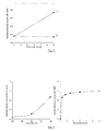
- Figure 1 (a) shows the physical thickness variation of the as deposited gate dielectrics upon anneal at different temperatures.
- Figure 1 (b) shows the thickness variation of the as deposited ALD La 2 0 3 upon different anneal steps approximately from 600°C to 1000°C.
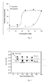
- Figure 2 shows the normalized thickness increase (t annealed - t dep )/t dep for DyScO x layers annealed in O 2 (•: circle) or N 2 (A: triangle), where t annealed is the layer thickness after a thermal anneal at about 1000°C and t dep is the as-deposited thickness of the layer.
- Figure 3 shows the normalized thickness increase for an about 10 nm DyScO x layer after different thermal treatments (temperature and time).
- Figure 4 shows the normalized thickness increase (t annealed - t dep )/t dep (•: circle) and absolute thickness increase (A: triangle) after 1000°C anneal for a DyScOx layer as function of the as-deposited thickness.
- Figure 5 shows the normalized thickness increase (t annealed - t dep )/t dep after a 1000°C anneal for DyScOx layers as function of the anneal time: Dy-rich (about 75%Dy) (•: circle); Sc-rich (about 25%Dy) ( ⁇ : square) .
- Figure 6 shows the relative thickness increase (%) as function of the Dy concentration (%) for two different compounds: DyHfOx ( ⁇ : square) and DyScOx (•: circle).
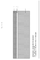
- Figure 7 presents the threshold voltage (Vt) shift for Dy-based and Sc-based oxides and a combination thereof.
- Figure 9 shows the effects of Dy 2 O 3 cap thicknesses on the EOT of SiON/Dy 2 O 3 /TaN.
- Figure 10 shows the EOT and eWF of SiO(N)/Dy 2 O 3 /TaN as a function of Dy 2 O 3 / (Dy 2 O 3 +SiO (N)) thickness ratio.
- Figure 11 shows hte EOT and eWF of SiO(N)/Dy 2 O 3 /TaN with various thermal budgets and annealing sequences.
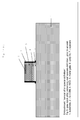
- Figure 12 illustrates different aspects of a method of the invention:
- the present invention provides a method for forming a gate stack in a MOSFET device, comprising the steps of:
- the present invention is based on the surprising discovery that the best results in terms of EOT reduction (Equivalent Oxide Thickness reduction) and eWF shift (effective work function shift) are obtained when the anneal (for said RES formation) step takes place only after the metal gate electrode has been deposited on said REO.
- the present invention is further based on the surprising discovery that there is an optimum ratio REO/(REO +SiCDM) for which the EOT is the lowest (see fig. 9 ). Indeed, a second unexpected observation was the increase of the EOT when departing away from that optimum REO/(REO +Si-CDM) ratio.
- Fig. 9 shows the effect of Dy 2 O 3 thickness on the EOT of SiON/Dy 2 O 3 stacks with a fixed SiON thickness (2 nm).
- the experiment result shows that the EOT actually decreases from 1.8 nm to 1.4 nm (18 to 14 ⁇ ) when the SiON is capped with 0.5- and 1-nm Dy 2 O 3 .
- the optimal Dy 2 O 3 /(Dy 2 O 3 +SiO 2 ) thickness ratio for minimal EOT is comprised between 0.2 and 0.4.
- Fig. 10 shows the effect of Dy 2 O 3 /(Dy 2 O 3 +SiO 2 ) thickness ratio thickness on the EOT of SiON/Dy 2 O 3 stacks with a fixed total Dy 2 O 3 +SiO 2 thickness (3 nm).
- the EOT of the SiO 2 /Dy 2 O 3 stack is a function of the Dy 2 O 3 /(Dy 2 O 3 +SiO 2 ) thickness ratio.
- the smallest EOT is obtained at a ratio comprised between about 0.3 and about 0.4, corresponding to an EOT reduction of 0.5 nm (5 ⁇ ) as compared to the uncapped SiO 2 .
- the effective work function (eWF) is inversely proportional to the ratio.
- the eWF decreases from 4.4 to 3.7 eV as the Dy 2 O 3 /(Dy 2 O 3 +SiO 2 ) thickness ratio increases from 0 to 0.7, and stabilizes at 3.7 eV with a ratio higher than 0.7.
- the optimal Dy 2 O 3 / (Dy 2 O 3 +SiO 2 ) thickness ratio is about 0.3 where the EOT reduction is maximized and the eWF is comparable to that of the SiON/poly reference (4.0 eV).
- Fig. 10 also shows that when nitrogen is added in SiO 2 , the EOT and eWF decrease by 0.2 nm (2 ⁇ ) and 150 mV, respectively, as compared to the SiO 2 /Dy 2 O 3 stack at the same the Dy 2 O 3 /(Dy 2 O 3 +SiO 2 ) thickness ratio.
- the EOT decrease may result from an increased dielectric constant or enhanced Dy 2 O 3 -SiO(N) intermixing due to the nitrogen incorporation.
- the eWF decrease may result from the positive charges induced by the nitrogen incorporation which was also seen on the HfSiO(N)/Ta 2 C stack.
- Fig. 11 shows the EOT and the eWF of Dy 2 O 3 -capped SiON from various thermal budgets and annealing sequences.
- S/D RTA standard activation anneal
- PDA post-deposition anneal
- a method of the invention for forming a gate stack in a MOSFET device comprises the steps of:
- said annealing step is performed at a temperature preferably comprised between 600°C and 1200°C, more preferably comprised between 600°C and 1000°C.
- said REO and said SiO 2 are provided in a ratio REO: (REO + SiO 2 ) comprised between 0.1 and 0.4, more preferably between 0.2 and 0.4, and even more preferably between 0.2 and 0.3.
- Said REO layer can be formed or deposited by MOCVD, ALD, AVD or PVD deposition technique.
- Said SiO 2 or SiON layer can be formed or deposited by MOCVD, ALD, AVD or PVD deposition technique.
- Said SiO 2 or SiON layer can further comprise Sc, Hf or Al.
- said REO layer can further comprise Sc, Hf or Al.
- both REO layer and SiO 2 (or SiON) layer can further comprise Sc, Hf or Al.
- said metal gate electrode can comprise (or consist of) W, Ta, Ti, Ru, Pt and/or Mo, more particularly can comprise (or consist of) TiN, TaN and/or Ru.
- said substrate can comprise (or consist of) a Ge, SiGe, GaAs, and/or InP layer.
- Said annealing step can be a post-deposition anneal or a RTA step.
- An object of the present invention is also a semiconductor device, more particularly a MOSFET device obtainable by a preferred method of the invention.
- a preferred MOSFET device of the invention comprises:
- Said RES layer results from the annealing of the SiO 2 or SiON layer and the REO layer (comprising Dy and/or La) that are deposited (or formed) upon said substrate, said annealing being performed only after having deposited said metal gate electrode.
- Said SiO 2 or SiON layer can further comprise Sc, Hf or Al.
- said RES layer can further comprise Sc, Hf or Al.
- both RES layer and SiO 2 (or SiON) layer can further comprise Sc, Hf or Al.
- Said metal gate electrode can comprise (or consist of) W, Ti, Ta, Pt, Ru and/or Mo, preferably can comprise (or consist of) TiN, TaN and/or Ru.
- Said substrate can comprise (or consist of) a Ge, SiGe, GaAs, and/or InP layer.
- Figure 1 (a) shows the physical thickness variation of the as deposited gate dielectrics upon anneal at different temperatures. On the X-axis are the ellipsometrically measured film thicknesses for the various gate dielectrics.
- Various deposition techniques like Atomic layer Deposition (ALD) and Atomic Vapor Deposition (AVD) have been employed.
- the films have been deposited on an interfacial SiO 2x silicon oxide like interface, which is not distinguishable from the ellipsometer result.
- the deposited bi-layer film stack has been annealed at temperatures approximately between 600°C and 1000°C in O 2 , the later to explicitly stimulate the film thickness increase.
- the bar graph for IMEC-clean indicates the silicon substrate oxidation as function of anneal treatment studied (reference).
- the IMEC-clean is a wet cleaning sequence comprising the steps of organic removal with SOM (Sulphuric acid- Ozone mixture), followed by APM (ammonium peroxide) cleaning and diluted HF/HC1 with DI (deionized) water rinses in between and Marangoni drying at the end. This substrate only received a clean thereby forming a chemical oxide.
- the thickness increase/layer reaction is thermally activated, the larger the thermal budget the larger the physical thickness, and fully deploying at temperatures of approximately 1000°C or above.
- the degree of reactivity i.e. the dependency of physical thickness on thermal budget, clearly depends on the species involved, with Dy (and La, see Fig 1(b) ) reacting more substantial than Sc (or even Si) containing films.
- the reactivity of the Dy containing films can be modulated with Sc addition.
- Figure 1 (b) shows the thickness variation of the as deposited ALD La 2 O 3 upon different anneal steps approximately from 600°C to 1000°C. Similar as for Dy, also for La a clear reactivity and hence physical thickness increase can be observed upon thermal annealing. However, as can be seen from Figure 1 (b) , La 2 O 3 shows a different behavior compared to Dy:
- the (rare earth) element used is one of the parameters that assist in controlling the dielectric properties of the final gate dielectric layer outcome at the end of the process.
- silicate formation When annealing a rare earth oxide (REO) layer or stack of layers deposited on top of silicon oxide , silicate formation can be witnessed for example as:
- REO rare earth oxide
- Figure 2 shows the normalized thickness increase (t annealed - t dep )/t dep for DyScO x layers annealed in O 2 (•: circle) or N 2 (A: triangle), where t annealed is the layer thickness after a thermal anneal at about 1000°C and t dep is the as-deposited thickness of the layer.
- the silicate formation is function of the thermal budget applied, i.e. depends on time as well as temperature, as shown in Figure 3 .
- Figure 3 shows the normalized thickness increase for an about 10 nm DyScO x layer after different thermal treatments (temperature and time).
- Figure 4 shows the normalized thickness increase (t annealed - t dep )/t dep (•: circle) and absolute thickness increase (A: triangle) after 1000°C anneal for a DyScOx layer as function of the as-deposited thickness.
- Figure 5 shows the normalized thickness increase (t annealed - t dep )/t dep after a 1000°C anneal for DyScOx layers as function of the anneal time: Dy-rich (about 75%Dy) (•: circle); Sc-rich (about 25%Dy) ( ⁇ : square).
- Figure 6 shows the relative thickness increase (%) as function of the Dy concentration (%) for two different compounds: DyHfOx ( ⁇ : square) and DyScOx (•: circle).
- DyScO x layers rather behave as Dy 2 O 3 layers (extensive silicate formation) except for the more Sc-rich layers, incorporation of Hf is clearly seen to limit the silicate formation (less thickness increase since less SiO 2 incorporation) up to the very Dy-rich DyHfOx layers.
- silicate formation can only occur by mixing of the RE oxide with the SiO 2 present in the underlying layer. This mixing results in a drop of the density of the RE oxide. This density drop is proportional to the ratio of RE/SiO 2 .
- the ideal metal gate needs a tunable work function with process conditions "similar" to classical silicon technologies. This implicitly suggests gaining control of the interface polarization between the metal and the dielectric to engineer the gate work function.
- Results indicate that Al can be used to shift the threshold voltage upwards (of interest for PMOS), as opposed to rare earth elements that were found to shift the threshold voltage to lower values (of interest for NMOS).
- Dy-based oxides show unexpectedly good results when implemented as cap layers.
- Figure 7 presents the threshold voltage shift for Dy-based and Sc-based oxides and a combination thereof.
- the magnitude of the effect is the result of a complex equation with for example the composition of the gate dielectric and metal gate as input parameters.
- the SiO 2 thickness can be controlled through thermal oxidation of the substrate prior to any high-k deposition.
- the various nanometer thick high-k dielectric films can be deposited by a range of techniques - preferably chemical vapor deposition like, either as nanolaminates or as co-deposited films.
- the composition of the film can be controlled.
- the thickness of SiO 2 and composition/thickness of the high-k films ought to be selected such that after application of a thermal budget, a suitable EOT is obtained.
- a SiON dielectric film of thickness 2nm has been capped by 1nm of Dy 2 O 3 and capped with a TaN metal electrode as shown in Figure 8 (a) .
- a junction activation thermal budget (1030°C)
- a gate stack EOT has been extracted, clearly less than the original 2nm SiON.
- a reduction in EOT from ⁇ 1.8nm down to 1.3nm EOT has been observed, as well as a reduction in Vt as shown in Figure 8 (b) .
- a similar experiment has been done using HfSiON dielectrics with Dy 2 O 3 cap.
Landscapes
- Insulated Gate Type Field-Effect Transistor (AREA)
- Semiconductor Integrated Circuits (AREA)
Priority Applications (3)
| Application Number | Priority Date | Filing Date | Title |
|---|---|---|---|
| EP07113225A EP1944794A1 (de) | 2007-01-10 | 2007-07-26 | Verfahren zur kontrollierten Erzeugung eines Gate-Dielektrikumstapels |
| JP2008002390A JP2008198995A (ja) | 2007-01-10 | 2008-01-09 | ゲートの誘電性スタックの制御された形成方法 |
| US11/972,615 US20080308881A1 (en) | 2007-01-10 | 2008-01-10 | Method for Controlled Formation of a Gate Dielectric Stack |
Applications Claiming Priority (3)
| Application Number | Priority Date | Filing Date | Title |
|---|---|---|---|
| US87969307P | 2007-01-10 | 2007-01-10 | |
| EP07111486 | 2007-06-29 | ||
| EP07113225A EP1944794A1 (de) | 2007-01-10 | 2007-07-26 | Verfahren zur kontrollierten Erzeugung eines Gate-Dielektrikumstapels |
Publications (1)
| Publication Number | Publication Date |
|---|---|
| EP1944794A1 true EP1944794A1 (de) | 2008-07-16 |
Family
ID=38480884
Family Applications (1)
| Application Number | Title | Priority Date | Filing Date |
|---|---|---|---|
| EP07113225A Withdrawn EP1944794A1 (de) | 2007-01-10 | 2007-07-26 | Verfahren zur kontrollierten Erzeugung eines Gate-Dielektrikumstapels |
Country Status (3)
| Country | Link |
|---|---|
| US (1) | US20080308881A1 (de) |
| EP (1) | EP1944794A1 (de) |
| JP (1) | JP2008198995A (de) |
Families Citing this family (4)
| Publication number | Priority date | Publication date | Assignee | Title |
|---|---|---|---|---|
| KR100994995B1 (ko) * | 2007-08-07 | 2010-11-18 | 삼성전자주식회사 | DySc03 막을 포함하는 반도체 박막의 적층 구조 및 그 형성방법 |
| US8313994B2 (en) * | 2009-03-26 | 2012-11-20 | Tokyo Electron Limited | Method for forming a high-K gate stack with reduced effective oxide thickness |
| JP2012038816A (ja) * | 2010-08-04 | 2012-02-23 | Fujitsu Semiconductor Ltd | 半導体装置の製造方法 |
| KR20120107762A (ko) | 2011-03-22 | 2012-10-04 | 삼성전자주식회사 | 반도체 소자의 제조 방법 |
Citations (2)
| Publication number | Priority date | Publication date | Assignee | Title |
|---|---|---|---|---|
| WO2001054200A1 (en) * | 2000-01-19 | 2001-07-26 | North Carolina State University | Lanthanum oxide-based gate dielectrics for integrated circuit field effect transistors and methods of fabricating same |
| US20020005556A1 (en) * | 1999-10-06 | 2002-01-17 | Eduard Albert Cartier | Silicate gate dielectric |
Family Cites Families (9)
| Publication number | Priority date | Publication date | Assignee | Title |
|---|---|---|---|---|
| US6281102B1 (en) * | 2000-01-13 | 2001-08-28 | Integrated Device Technology, Inc. | Cobalt silicide structure for improving gate oxide integrity and method for fabricating same |
| CA2360312A1 (en) * | 2000-10-30 | 2002-04-30 | National Research Council Of Canada | Novel gate dielectric |
| WO2005004198A2 (en) * | 2003-06-13 | 2005-01-13 | North Carolina State University | Complex oxides for use in semiconductor devices and related methods |
| US7074680B2 (en) * | 2004-09-07 | 2006-07-11 | Intel Corporation | Method for making a semiconductor device having a high-k gate dielectric |
| JP4185056B2 (ja) * | 2005-01-26 | 2008-11-19 | 株式会社東芝 | 絶縁膜、および半導体装置 |
| US7824990B2 (en) * | 2005-12-05 | 2010-11-02 | Taiwan Semiconductor Manufacturing Company, Ltd. | Multi-metal-oxide high-K gate dielectrics |
| US7611972B2 (en) * | 2006-11-29 | 2009-11-03 | Qimonda North America Corp. | Semiconductor devices and methods of manufacture thereof |
| EP1944801A1 (de) * | 2007-01-10 | 2008-07-16 | Interuniversitair Microelektronica Centrum | Verfahren zur Herstellung einer CMOS-Vorrichtung mit dualer Austrittsarbeit |
| KR100994995B1 (ko) * | 2007-08-07 | 2010-11-18 | 삼성전자주식회사 | DySc03 막을 포함하는 반도체 박막의 적층 구조 및 그 형성방법 |
-
2007
- 2007-07-26 EP EP07113225A patent/EP1944794A1/de not_active Withdrawn
-
2008
- 2008-01-09 JP JP2008002390A patent/JP2008198995A/ja active Pending
- 2008-01-10 US US11/972,615 patent/US20080308881A1/en not_active Abandoned
Patent Citations (2)
| Publication number | Priority date | Publication date | Assignee | Title |
|---|---|---|---|---|
| US20020005556A1 (en) * | 1999-10-06 | 2002-01-17 | Eduard Albert Cartier | Silicate gate dielectric |
| WO2001054200A1 (en) * | 2000-01-19 | 2001-07-26 | North Carolina State University | Lanthanum oxide-based gate dielectrics for integrated circuit field effect transistors and methods of fabricating same |
Non-Patent Citations (4)
| Title |
|---|
| ALSHAREEF H N ET AL: "Thermally stable N-metal gate MOSFETs using La-incorporated HfSiO dielectric", 2006 SYMPOSIUM ON VLSI TECHNOLOGY (IEEE CAT. NO. 06CH37743C) IEEE PISCATAWAY, NJ, USA, 2006, pages 2 pp., XP002460662, ISBN: 1-4244-0004-X * |
| ALSHAREEF H N ET AL: "Work function engineering using lanthanum oxide interfacial layers", APPLIED PHYSICS LETTERS AIP USA, vol. 89, no. 23, 4 December 2006 (2006-12-04), pages 232103 - 1, XP002460661, ISSN: 0003-6951 * |
| L. PANTISANO ET AL., APPL. PHYS. LETT., vol. 89, 2006, pages 113505 |
| VAN ELSHOCHT S ET AL: "Metallorganic chemical vapor deposition of dysprosium scandate high-k layers using mmp-type precursors", JOURNAL OF THE ELECTROCHEMICAL SOCIETY ELECTROCHEM. SOC USA, vol. 153, no. 9, September 2006 (2006-09-01), pages F219 - F224, XP002460663, ISSN: 0013-4651 * |
Also Published As
| Publication number | Publication date |
|---|---|
| US20080308881A1 (en) | 2008-12-18 |
| JP2008198995A (ja) | 2008-08-28 |
Similar Documents
| Publication | Publication Date | Title |
|---|---|---|
| US7884423B2 (en) | Semiconductor device and fabrication method thereof | |
| US7952118B2 (en) | Semiconductor device having different metal gate structures | |
| US20090020836A1 (en) | Method for making a semiconductor device having a high-k gate dielectric | |
| CN102714177B (zh) | 具有带氧阻障层的金属栅极堆叠的场效应晶体管器件 | |
| Guha et al. | High-κ/metal gate science and technology | |
| US20080224238A1 (en) | ADVANCED HIGH-k GATE STACK PATTERNING AND STRUCTURE CONTAINING A PATTERNED HIGH-k GATE STACK | |
| CN101156246A (zh) | 用于高性能CMOS应用的超薄Hf掺杂氮氧化硅膜及制造方法 | |
| KR20090011463A (ko) | 고압 산소 열처리를 통한 반도체 소자의 제조방법 | |
| US20060289948A1 (en) | Method to control flatband/threshold voltage in high-k metal gated stacks and structures thereof | |
| US20090050982A1 (en) | Method for Modulating the Effective Work Function | |
| Wilk et al. | Improved film growth and flatband voltage control of ALD HfO/sub 2/and Hf-Al-O with n/sup+/poly-Si gates using chemical oxides and optimized post-annealing | |
| US20100006954A1 (en) | Transistor device | |
| US7402472B2 (en) | Method of making a nitrided gate dielectric | |
| EP1944794A1 (de) | Verfahren zur kontrollierten Erzeugung eines Gate-Dielektrikumstapels | |
| US7635634B2 (en) | Dielectric apparatus and associated methods | |
| US8609522B2 (en) | Process for producing a conducting electrode | |
| Tseng et al. | The progress and challenges of threshold voltage control of high-k/metal-gated devices for advanced technologies | |
| EP1880409B1 (de) | Verfahren zum herstellen eines mos-bauelements mit einem high-k gate-dielektrikum oder sion | |
| CN101308788A (zh) | 半导体装置及其制造方法 | |
| Rittersma et al. | Characterization of Thermal and Electrical Stability of MOCVD HfO2 HfSiO4 Dielectric Layers with Polysilicon Electrodes for Advanced CMOS Technologies | |
| US20080308896A1 (en) | Integrated circuit device comprising a gate electrode structure and corresponding method of fabrication | |
| EP2081232B1 (de) | Interpoly-Dielektrikumstapel mit verbesserter Immunität | |
| JP2006269520A (ja) | 半導体装置およびその製造方法 | |
| JP4997809B2 (ja) | 半導体装置および半導体装置の製造方法 | |
| Swerts et al. | Highly scalable ALD-deposited hafnium silicate gate stacks for low standby power applications |
Legal Events
| Date | Code | Title | Description |
|---|---|---|---|
| PUAI | Public reference made under article 153(3) epc to a published international application that has entered the european phase |
Free format text: ORIGINAL CODE: 0009012 |
|
| AK | Designated contracting states |
Kind code of ref document: A1 Designated state(s): AT BE BG CH CY CZ DE DK EE ES FI FR GB GR HU IE IS IT LI LT LU LV MC MT NL PL PT RO SE SI SK TR |
|
| AX | Request for extension of the european patent |
Extension state: AL BA HR MK RS |
|
| 17P | Request for examination filed |
Effective date: 20080829 |
|
| 17Q | First examination report despatched |
Effective date: 20081006 |
|
| AKX | Designation fees paid |
Designated state(s): AT BE BG CH CY CZ DE DK EE ES FI FR GB GR HU IE IS IT LI LT LU LV MC MT NL PL PT RO SE SI SK TR |
|
| RAP1 | Party data changed (applicant data changed or rights of an application transferred) |
Owner name: TAIWAN SEMICONDUCTOR MANUFACTURING CO., LTD. Owner name: IMEC |
|
| STAA | Information on the status of an ep patent application or granted ep patent |
Free format text: STATUS: THE APPLICATION IS DEEMED TO BE WITHDRAWN |
|
| 18D | Application deemed to be withdrawn |
Effective date: 20121211 |