EP1947842B1 - Capteurs d'images avec mécanismes de réduction d'éblouissement - Google Patents
Capteurs d'images avec mécanismes de réduction d'éblouissement Download PDFInfo
- Publication number
- EP1947842B1 EP1947842B1 EP07150484.9A EP07150484A EP1947842B1 EP 1947842 B1 EP1947842 B1 EP 1947842B1 EP 07150484 A EP07150484 A EP 07150484A EP 1947842 B1 EP1947842 B1 EP 1947842B1
- Authority
- EP
- European Patent Office
- Prior art keywords
- pixels
- row
- exposure period
- rows
- reading out
- Prior art date
- Legal status (The legal status is an assumption and is not a legal conclusion. Google has not performed a legal analysis and makes no representation as to the accuracy of the status listed.)
- Active
Links
Images


Classifications
-
- H—ELECTRICITY
- H10—SEMICONDUCTOR DEVICES; ELECTRIC SOLID-STATE DEVICES NOT OTHERWISE PROVIDED FOR
- H10F—INORGANIC SEMICONDUCTOR DEVICES SENSITIVE TO INFRARED RADIATION, LIGHT, ELECTROMAGNETIC RADIATION OF SHORTER WAVELENGTH OR CORPUSCULAR RADIATION
- H10F39/00—Integrated devices, or assemblies of multiple devices, comprising at least one element covered by group H10F30/00, e.g. radiation detectors comprising photodiode arrays
- H10F39/10—Integrated devices
- H10F39/12—Image sensors
- H10F39/18—Complementary metal-oxide-semiconductor [CMOS] image sensors; Photodiode array image sensors
- H10F39/186—Complementary metal-oxide-semiconductor [CMOS] image sensors; Photodiode array image sensors having arrangements for blooming suppression
-
- H—ELECTRICITY
- H04—ELECTRIC COMMUNICATION TECHNIQUE
- H04N—PICTORIAL COMMUNICATION, e.g. TELEVISION
- H04N25/00—Circuitry of solid-state image sensors [SSIS]; Control thereof
-
- H—ELECTRICITY
- H04—ELECTRIC COMMUNICATION TECHNIQUE
- H04N—PICTORIAL COMMUNICATION, e.g. TELEVISION
- H04N25/00—Circuitry of solid-state image sensors [SSIS]; Control thereof
- H04N25/50—Control of the SSIS exposure
- H04N25/53—Control of the integration time
- H04N25/533—Control of the integration time by using differing integration times for different sensor regions
-
- H—ELECTRICITY
- H04—ELECTRIC COMMUNICATION TECHNIQUE
- H04N—PICTORIAL COMMUNICATION, e.g. TELEVISION
- H04N25/00—Circuitry of solid-state image sensors [SSIS]; Control thereof
- H04N25/50—Control of the SSIS exposure
- H04N25/57—Control of the dynamic range
- H04N25/58—Control of the dynamic range involving two or more exposures
- H04N25/587—Control of the dynamic range involving two or more exposures acquired sequentially, e.g. using the combination of odd and even image fields
- H04N25/589—Control of the dynamic range involving two or more exposures acquired sequentially, e.g. using the combination of odd and even image fields with different integration times, e.g. short and long exposures
-
- H—ELECTRICITY
- H04—ELECTRIC COMMUNICATION TECHNIQUE
- H04N—PICTORIAL COMMUNICATION, e.g. TELEVISION
- H04N25/00—Circuitry of solid-state image sensors [SSIS]; Control thereof
- H04N25/60—Noise processing, e.g. detecting, correcting, reducing or removing noise
- H04N25/62—Detection or reduction of noise due to excess charges produced by the exposure, e.g. smear, blooming, ghost image, crosstalk or leakage between pixels
- H04N25/621—Detection or reduction of noise due to excess charges produced by the exposure, e.g. smear, blooming, ghost image, crosstalk or leakage between pixels for the control of blooming
- H04N25/623—Detection or reduction of noise due to excess charges produced by the exposure, e.g. smear, blooming, ghost image, crosstalk or leakage between pixels for the control of blooming by evacuation via the output or reset lines
Definitions
- the present disclosure relates to image sensors having blooming reduction mechanisms.
- aspects of the present disclosure relate to complementary metal oxide silicon (CMOS) image sensors having increased dynamic range and reduced blooming characteristics.
- CMOS complementary metal oxide silicon
- image sensors Unlike traditional cameras that use films to capture and store images, today's digital cameras use solid-state image sensors to acquire images. Such image sensors are typically disposed on fingernail-sized silicon chips containing millions of photoelectric devices such as photodiodes arranged in an array of pixels. During exposure, each photoelectric device records intensity or brightness of an incident light by converting optical energy into accumulated electrical charges. The brightness recorded by each photoelectric device can then be read out and stored as digital signals.
- Dynamic range is the ratio of maximum and minimum light intensities that an image sensor can capture.
- the charge holding capacity of each photoelectric device in the image sensor typically determines its dynamic range.
- the limited capacity of each photoelectric device limits the image sensor's ability to capture bright and dark subjects at the same time.
- the patent document JP 2006253876 describes a CMOS image sensor in which pixels belonging to even rows and odd rows have different sensitivities/gains, obtained by means of different exposure times. As a result, if a long exposure is used to capture dark subjects, bright subjects can lose contrast and become a bright spot. If a short exposure is used to capture bright subjects, dark subjects can blend into a dark background and simply disappear.
- Blooming occurs when a photoelectric device of the image sensor overflows and spills accumulated charges (e.g., electrons) into neighboring photoelectric devices
- the spilled charges can distort the brightness recorded by the neighboring photoelectric devices and ultimately reduce spatial resolution.
- the brightness recorded by a neighboring photoelectric device can be falsely high due to the spilled charges.
- the bright subjects causing blooming often appear to have a "glow" around them in a captured image.
- a known approach to avoid blooming is described by the International patent application WO2004/074789 . It describes a CMOS image sensor operating with short and long integration times. In each pixel two different integration capacitances provide for different gains. An anti-bloom transistor is also provided for in each pixel.
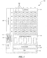
- FIG. 1 schematically illustrates an image sensor 100 with a blooming reduction mechanism and configured in accordance with an embodiment of the invention.
- the image sensor 100 can include a pixel array 101, a column-select circuit 106, a row-select circuit 108, analog signal processors 104, a timing and control circuit 110, an A/D converter 112, and a digital signal processor (DSP) 114. These components can be disposed on a single substrate 103 (e.g., a semiconductor chip) or can be disposed on multiple substrates.
- a single substrate 103 e.g., a semiconductor chip
- the pixel array 101 can include a plurality of pixels 102 arranged in columns and rows.
- the pixel array 101 includes six columns and six rows designated rows L0, S0, L1, S1, L2, and S2 and columns 1 to 6.
- row L0 includes pixels L00-L05
- row S0 includes pixels S00-S05.
- the pixels in rows L0, L1, and L2 are configured for a long exposure period (e.g., 2 seconds), and those in rows S0, S1, and S2 are configured for a short exposure period (e.g., 0.1 seconds).
- rows L0, L1, and L2 are referred to as long exposure rows
- rows S0, S1, and S2 are referred to as short exposure rows hereinafter.
- Individual pixels 102 can be configured as a charged coupled device, a CMOS passive pixel sensor, a CMOS active pixel sensor, or other types of light sensors.
- the pixels 102 can be configured as 4T CMOS active pixels as described in more detail below with reference to Figure 2 .
- the pixels 102 in the long exposure rows are configured to be generally identical to those in the short exposure rows.
- the pixels 102 in the long exposure rows can be configured to be different than those in the short exposure rows.
- the pixels 102 in rows L0, L1, and L2 can include photosites having a larger well capacity than those in rows S0, S1, and S2.
- the timing and control circuit 110 can include a microprocessor-based processor 111 containing logic modules for monitoring and controlling the exposure and readout sequence of the pixels 102.
- the processor 111 can include an 8080, 8085, 8086, or other type of logic processor produced by Intel, Corp. of Santa Clara, California.
- the timing and control circuit 110 can also include logic modules configured to reduce overexposure blooming by varying the exposure and readout sequence of the pixels 102, as described in more detail below with reference to Figure 2 .
- the column-select circuit 106 and the row-select circuit 108 can include solid-state switches including, for example, metal oxide silicon (MOS), CMOS, or other types of solid-state switch.
- MOS metal oxide silicon
- CMOS complementary metal oxide silicon
- the column-select circuit 106 and the row-select circuit 108 can decode signals sampled from the pixels 102 by selectively enabling output from each column and row of the pixels 102.
- the analog signal processors 104 and/or the digital signal processor 114 can include input clamping, sampling, amplifying, multiplexing, filtering, or other types of circuits.
- the analog signal processors 104 can include source-follower transistors for amplifying sampled signals from the pixels 102
- the digital signal processor 114 can include a data compression circuit.
- the A/D converter 112 can include conversion circuits that convert analog signals from the pixels 102 into digital signals having a desired resolution (e.g., 8-bit, 16-bit, 32-bit, etc.)
- the timing and control circuit 110 controls exposure of individual rows of the pixel array 101 to an incident light by selectively turning on/off the row-select circuit 108 and the column-select circuit 106.
- the individual rows of the pixel array 101 can be exposed for different exposure periods. For example, rows L0, L1, and L2 are exposed for a long exposure period (e.g., 2 seconds), and rows S0, S1, and S2 are exposed for a short exposure period (e.g., 0.1 seconds).
- the pixels 102 convert the incident light into accumulated charges (e.g., electrons). Then the pixels 102 are sampled to generate analog output signals based on the amount of accumulated charges.
- the analog signal processors 104 then process the analog output signals before the A/D converter 112 converts them into digital output signals.
- the digital signal processor 114 then further processes the digital output signals into final output signals that can be displayed on a monitor or printed as a photo.
- One expected advantage of having different exposure periods for different rows of pixels 102 is the improved dynamic range of the image sensor 100.
- dark subjects can be clearly captured.
- another adjacent row of the pixels has a short exposure period, bright subjects can be captured.
- the captured dark and bright subjects can then be combined using histogram equalizing, weighted averaging, contrast blending, radiance mapping, or another suitable technique to derive a final image.
- the final image would have details for both the dark and bright subjects to improve the dynamic range of the image sensor 100.
- Figure 2 illustrates a pixel 102 suitable for use in the image sensor 100 of Figure 1 .
- the pixel 102 includes a photodiode 122 connected to a floating node 126 via a transfer transistor 124.
- the floating node 126 in turn is connected to a source-follower transistor 128 that can buffer a signal from the floating node 126.
- the output from the source-follower transistor 128 is connected to a column bitline 136 via a row-select transistor 130.
- the floating node 126 is also electrically connected to a reset transistor 132 whose source is connected to a reference voltage line 134 at a reference voltage V dd.
- the pixel 102 is configured as a four-transistor (4T) CMOS active pixel. In other embodiments, the pixel 102 can be configured as a 3T, 5T, 6T, or 7T CMOS or as a CCD pixel.
- 4T four-transistor
- the pixel 102 can be configured as a 3T, 5T, 6T, or 7T CMOS or as a CCD pixel.
- the reset transistor 132 is first turned on to set the floating node 126 to the reference voltage V dd . Then the transfer transistor 124 is turned on to transfer the accumulated charges from the photodiode 122 to the floating node 126. As a result, the floating node 126 acquires a new voltage, and the photodiode 122 is reset. The source-follower transistor 128 then buffers the new voltage at the floating node 126 onto the column bitline 136. In certain embodiments, before the photodiode 122 is exposed to an incident light, the transfer transistor 124 and the reset transistor 132 can be turned on to reset the photodiode 122.
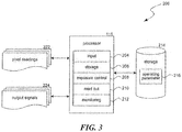
- FIG. 3 illustrates a functional diagram showing logic modules 200 of the timing and control circuit 110 suitable for use in the image sensor 100.
- Each module can be a computer program, procedure, or process written as source code in a conventional programming language, such as the C++ programming language, and can be presented for execution by the processor 111 of the timing and control circuit 110.
- Each module can also be implemented as individual electrical circuits.
- the various implementations of the source code and object and byte codes can be stored on a computer-readable storage medium or embodied on a transmission medium in a carrier wave.
- the modules of the timing and control circuit 110 can include an input module 204, a storage module 206, an exposure control module 208, a readout module 210, and a monitoring module 212.
- the input module 204 accepts input, such as pixel readings 222 (e.g., pixel output voltage), and communicates the accepted information to other components for further processing.
- the storage module 206 organizes records including, for example, operating parameters 216, and facilitates storing and retrieving of these records to and from a storage 214 (e.g., a flash memory module, an EPROM, or other storage device). Any type of record organization can be utilized, including a flat file system, hierarchical database, relational database, or distributed database.
- the exposure control module 208 can control an exposure sequence of the pixels 102 by, for example, causing each row of pixels 102 to be exposed to an incident light sequentially. For instance, the exposure control module 208 can cause row L0 to be exposed before row S0 is exposed, or can cause row L0 and S0 to be exposed at the same time. In one embodiment, the exposure control module 208 can also implement asynchronous sequential exposure of the long exposure rows and the short exposure rows. For example, the long exposure rows can be exposed sequentially starting from a time To. After a preset time period ⁇ T, the short exposure rows are exposed sequentially. In other embodiments, the exposure control module 208 can implement synchronous sequential exposure of the long and short exposure rows. For example, the short exposure rows can be exposed only after all the long exposure rows have been exposed.
- the readout module 210 can control a readout sequence of the pixels 102 by, for example, sending output signals 224 to the column-select and row-select circuits 106, 108.
- the readout module 210 can be configured to scan each row of the pixel array 101 sequentially.
- the readout module 210 can cause the rows to be scanned in a regular scanning sequence as follows:
- the monitoring module 212 can generate control variables based on the pixel readings 222. For example, the monitoring module 212 can compare the pixel readings 222 (e.g., sensed light intensity) of the pixels 102 ( Figure 1 ) to a preset threshold value to determine whether the pixels 102 are overexposed. If the sensed light intensity exceeds the preset threshold value, the monitoring module 212 indicates overexposure, and the readout and/or exposure control modules 210, 208 can modify the readout and/or exposure sequence to reduce the blooming effect. For example, if the monitoring module 212 indicates that there is no overexposure, then the regular scanning sequence can be used; otherwise, an overexposure readout sequence can be used, as described in more detail below with reference to Figure 4 .
- the regular scanning sequence can be used; otherwise, an overexposure readout sequence can be used, as described in more detail below with reference to Figure 4 .
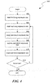
- Figure 4 illustrates a flow diagram showing a method 300 for operating the image sensor 100 of Figure 1 for blooming reduction.
- the first long exposure row L0 can be read out after row L0 has been exposed for a first exposure period (block 302).
- reading the pixels 102 of row L0 can include turning on the transfer transistor 124 to transfer accumulated charges from the photodiode 122 to the floating node 126.
- the photodiode 122 is now reset (i.e., having a voltage generally equal to a reference voltage).
- the successive long exposure row i.e., row L1
- Row L1 can be exposed generally simultaneously as the row L0 or can be exposed after row L0 has been read out.
- the photodiode 122 of each pixel 102 in row L1 is also reset.
- the first successive short exposure row i.e., row S0
- the first successive short exposure row i.e., row S0
- the first successive short exposure row i.e., row S0
- the pixels 102 in row S0 can be read out (block 310).
- the process returns to block 304, and the remaining rows of pixels can be scanned in a scanning sequence as follows:
- One expected advantage of operating the image sensor 100 according to the process of Figure 4 is the reduced blooming potential of the pixels 102.
- rows L0 and L1 are long exposure rows, so the pixels 102 in these rows have a greater potential for blooming than those in short exposure rows S0, S1, and S2. Blooming of any pixel 102 in rows L0 and L1 can affect the short exposure row S0 because row S0 is adjacent to both row L0 and row L1.
- any spilled-over charges can be destroyed.
- the impact of any blooming in the long exposure rows L0 and L1 can be at least reduced.
- the dynamic range of the image sensor 100 can be increased.
- Another expected advantage of several embodiments of the illustrated process of Figure 4 is that the image quality produced by the image sensor 100 is not affected during normal dynamic range operations.
- the image sensor 100 in Figure 1 is illustrated as having pixels arranged in long and short exposure rows, in another embodiment, the image sensor 100 can include pixel subsets that have pixels located in different rows and/or columns as illustrated in Figure 5 .
- the image sensor 100 includes long exposure subsets L0, L1, and L2 and short exposure subsets S0, S1, and S2.
- Each subset can include pixels located in different rows and/or columns.
- subset L0 can include pixels L00 in the first row/first column and pixels L01 in the second row/second column.
- One expected advantage of having pixels in different rows and/or columns is that the impact of blooming in long exposure subsets L0, L1, and L2 to adjacent short exposure subsets can be at least reduced both column-wise and row-wise.
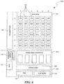
- FIG. 6 schematically illustrates an image sensor 500 with a blooming reduction mechanism and configured in accordance with another embodiment of the invention.
- the image sensor 500 can further include a line buffer 116 configured for temporarily holding pixel output from the pixel array 101.
- the line buffer 116 can be analog or digital.
- the line buffer 116 can include analog registers having capacitors for storing pixel output, or other suitable buffering components.
- the pixel array 101 of the image sensor 500 is arranged as rows 0-5 and columns 1-6.
- individual pixels 102 of the pixel array 101 are all configured to be generally identical.
- individual pixels 102 can be configured as 4T CMOS active pixels as described above with referenced to Figure 2 or as other types of CMOS or CCD pixels.
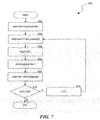
- Figure 7 illustrates a flow diagram showing a method 600 that can be implemented in the timing and control circuit 110 for operating the image sensor 500 of Figure 6 .
- the readout module 210 can cause row i (i is a positive integer, e.g., row 0) to be read after row i has been exposed for a first exposure period (block 602).
- the first exposure period can be configured to capture details of dark subjects of an image.
- row i+1 e.g., row 1
- the readout signals from row i and row i+1 can be buffered in the line buffer 116 ( Figure 5 ).
- row i+1 is read, row i is reset again to clear any spilled charges from row i+1 during the exposure for the first exposure period (block 606). Then row i is exposed again for a second exposure period (block 608). The second exposure period can be configured to capture details of bright subjects of the image. Then row i is read out again after the second exposure period expires (block 61 0).
- decision block 612 if there are more rows in the pixel array 10 1 , then the process returns to block 604 with i incremented by 1 (block 614); otherwise, the process ends.
- One expected advantage of operating the image sensor 500 according to the process illustrated in Figure 7 is the reduced blooming potential of the pixels 102.
- the method 6 0 0 includes reading out the pixels 102 in rows i+1 before resetting and exposing the previous row i.
- any spilled charges from row i+1 have been destroyed to at least reduce the blooming effect from row i+1.
- Another expected advantage is the increased dynamic range of the image sensor 500 because each row of the pixel array 101 is exposed twice to capture both dark and bright subjects of an image.
Landscapes
- Engineering & Computer Science (AREA)
- Multimedia (AREA)
- Signal Processing (AREA)
- Transforming Light Signals Into Electric Signals (AREA)
- Solid State Image Pick-Up Elements (AREA)
Claims (16)
- Un capteur d'images CMOS (100), comprenant :une pluralité de pixels (102) agencés en rangées (L0, L1, L2, S0, S1, S2), etun circuit de synchronisation et de commande (110) en communication électrique avec la pluralité de pixels, caractérisé en ce que le circuit de synchronisation et de commande comprend :un module de surveillance (212) destiné à la détermination si une première rangée de pixels est surexposée,un module de commande d'exposition (208) configuré de façon à mettre en oeuvre une séquence d'exposition qui comprend l'exposition d'une première rangée de pixels pendant une première période d'exposition, d'une deuxième rangée de pixels pendant une deuxième période d'exposition différente de la première période d'exposition et d'une troisième rangée de pixels pendant la première période d'exposition si le module de surveillance indique qu'il n'existe aucune surexposition dans la première rangée de pixels ou sinon de façon à mettre en oeuvre une séquence de lecture de surexposition destinée à la destruction d'une charge déversée, où la séquence de lecture de surexposition comprend la réinitialisation et l'exposition subséquente de la troisième rangée de pixels pendant la première période d'exposition, la réinitialisation et l'exposition subséquente de la deuxième rangée de pixels pendant la deuxième période d'exposition uniquement après la lecture de de la troisième rangée de pixels, où le module de commande d'exposition est configuré de façon à mettre en oeuvre la séquence de lecture de surexposition en réponse à la détermination que la première rangée est surexposée, la deuxième rangée de pixels étant disposée entre les première et troisième rangées de pixels, etun module de lecture (210) configuré de façon à mettre en oeuvre une séquence de balayage régulier qui comprend la lecture des première, deuxième et troisième rangées de pixels si le module de surveillance indique qu'il n'existe aucune surexposition dans la première rangée de pixels ou sinon de façon à mettre en oeuvre la séquence de lecture de surexposition qui comprend :la lecture de la première rangée de pixels exposée pendant la première période d'exposition,la lecture de la troisième rangée de pixels exposée pendant la première période d'exposition après la lecture de la première rangée de pixels, etensuite la lecture de la deuxième rangée de pixels exposée pendant la deuxième période d'exposition.
- Le capteur d'images CMOS selon la Revendication 1 où la deuxième période d'exposition est inférieure à la première période d'exposition.
- Le capteur d'images CMOS selon la Revendication 1 ou 2 où le module de lecture est également configuré de façon à(a) ensuite produire en sortie une autre rangée successive de pixels exposée pendant la première période d'exposition,(b) ensuite produire en sortie une autre rangée successive de pixels exposée pendant la deuxième période d'exposition, etla répétition des opérations (a)-(b) jusqu'à ce que la totalité des rangées de pixels soient produites en sortie.
- Le capteur d'images CMOS selon la Revendication 1 ou 2 où le module de lecture est configuré de façon à lire une première rangée de pixels après l'exposition de la première rangée de pixels mais avant l'exposition de la deuxième rangée de pixels.
- Le capteur d'images CMOS selon l'une quelconque des Revendications précédentes où le module de commande d'exposition est configuré de façon à exposer les première, deuxième et troisième rangées de pixels successivement.
- Le capteur d'images CMOS selon l'une quelconque des Revendications précédentes où le module de surveillance est configuré de façon à surveiller un signal produit en sortie à partir des première et deuxième rangées de pixels, à comparer le signal produit en sortie à une valeur seuil prédéfinie, et à indiquer une surexposition si le signal produit en sortie dépasse la valeur seuil prédéfinie.
- Un dispositif d'enregistrement d'images incorporant le capteur d'images CMOS selon l'une quelconque des Revendications précédentes, où le dispositif d'enregistrement d'images comprend au moins un dispositif parmi un appareil photo, un caméscope, un téléphone cellulaire, un enregistreur vidéo et un assistant numérique personnel.
- Un procédé de réduction de l'éblouissement dans un capteur d'images (100, 500) possédant une pluralité de pixels (102) agencés en rangées (L0, L1 L2, S0, S1, S2), le procédé étant caractérisé en ce qu'il comprend :l'exposition d'une première rangée de pixels pendant une première période d'exposition,la détermination si la première rangée de pixels est surexposée,l'exécution d'une séquence de balayage régulier qui comprend l'exposition subséquente et la lecture séquentielle d'une deuxième rangée de pixels pendant une deuxième période d'exposition différente de la première période d'exposition et d'une troisième rangée de pixels pendant la première période d'exposition s'il n'existe aucune surexposition dans la première rangée, ou sinonl'exécution d'une séquence de lecture de surexposition destinée à la destruction d'une charge déversée par la réinitialisation et l'exposition subséquente de la troisième rangée de pixels pendant la première période d'exposition, la réinitialisation et l'exposition subséquente de la deuxième rangée de pixels, qui est disposée entre les première et troisième rangées de pixels, pendant la deuxième période d'exposition, l'exposition de la troisième rangée de pixels étant en réponse au fait que la première rangée de pixels est surexposée, etla lecture de la première rangée de pixels exposée pendant la première période d'exposition,la lecture de la troisième rangée de pixels après la lecture de la première rangée de pixels, etensuite la lecture de la deuxième rangée de pixels exposée pendant la deuxième période d'exposition.
- Le procédé selon la Revendication 8 où l'exposition des première et deuxième rangées de pixels comprend l'exposition des première et deuxième rangées de pixels successivement.
- Le procédé selon la Revendication 8 où l'exposition des première et deuxième rangées de pixels comprend l'exposition des première et deuxième rangées de pixels généralement simultanément.
- Le procédé selon l'une quelconque des Revendications 8 à 10 où la deuxième période d'exposition est inférieure à la première période d'exposition.
- Le procédé selon l'une quelconque des Revendications 8 à 11 où la lecture de la première rangée de pixels comprend l'échantillonnage d'une tension à partir de pixels individuels de la première rangée et la réinitialisation des pixels sur une tension de référence.
- Le procédé selon l'une quelconque des Revendications 8 à 12, comprenant en outre :(a) ensuite la lecture d'une autre rangée successive de pixels exposée pendant la première période d'exposition, et(b) ensuite la lecture d'une autre rangée successive de pixels exposée pendant la deuxième période d'exposition.
- Le procédé selon la Revendication 13, comprenant en outre :la répétition des opérations (a)-(b) jusqu'à ce que la totalité des rangées de pixels soient lues.
- Le procédé selon la Revendication 8 où la lecture d'une première rangée de pixels comprend la lecture d'une première rangée de pixels après l'exposition de la première rangée de pixels mais avant l'exposition de la deuxième rangée de pixels.
- Le procédé selon l'une quelconque des Revendications 8 à 15 où la détermination si la première et/ou la deuxième rangée de pixels est surexposée comprend la surveillance d'un signal produit en sortie à partir des première et deuxième rangées de pixels et la comparaison du signal produit en sortie à une valeur seuil prédéfinie.
Applications Claiming Priority (1)
| Application Number | Priority Date | Filing Date | Title |
|---|---|---|---|
| US11/656,587 US7808538B2 (en) | 2007-01-22 | 2007-01-22 | Image sensors with blooming reduction mechanisms |
Publications (3)
| Publication Number | Publication Date |
|---|---|
| EP1947842A2 EP1947842A2 (fr) | 2008-07-23 |
| EP1947842A3 EP1947842A3 (fr) | 2010-11-24 |
| EP1947842B1 true EP1947842B1 (fr) | 2017-10-04 |
Family
ID=39322773
Family Applications (1)
| Application Number | Title | Priority Date | Filing Date |
|---|---|---|---|
| EP07150484.9A Active EP1947842B1 (fr) | 2007-01-22 | 2007-12-28 | Capteurs d'images avec mécanismes de réduction d'éblouissement |
Country Status (4)
| Country | Link |
|---|---|
| US (1) | US7808538B2 (fr) |
| EP (1) | EP1947842B1 (fr) |
| CN (1) | CN101232559B (fr) |
| TW (1) | TWI461060B (fr) |
Cited By (1)
| Publication number | Priority date | Publication date | Assignee | Title |
|---|---|---|---|---|
| DE102024100463A1 (de) | 2023-11-02 | 2025-05-08 | Semiconductor Components Industries, Llc | Beseitigung von blooming-artefakten bei der bildgebung mit hohem dynamikumfang |
Families Citing this family (32)
| Publication number | Priority date | Publication date | Assignee | Title |
|---|---|---|---|---|
| US7442629B2 (en) | 2004-09-24 | 2008-10-28 | President & Fellows Of Harvard College | Femtosecond laser-induced formation of submicrometer spikes on a semiconductor substrate |
| US7057256B2 (en) | 2001-05-25 | 2006-06-06 | President & Fellows Of Harvard College | Silicon-based visible and near-infrared optoelectric devices |
| US8395685B2 (en) * | 2008-07-07 | 2013-03-12 | The Charles Stark Draper Laboratory, Inc. | Wide dynamic range imaging sensor and method |
| JP5247397B2 (ja) * | 2008-12-05 | 2013-07-24 | キヤノン株式会社 | 撮像装置及び撮像方法 |
| US8970707B2 (en) * | 2008-12-17 | 2015-03-03 | Sony Computer Entertainment Inc. | Compensating for blooming of a shape in an image |
| US8144215B2 (en) * | 2009-05-11 | 2012-03-27 | Himax Imaging, Inc. | Method and apparatus of using processor with analog-to-digital converter within image sensor to achieve high dynamic range of image sensor |
| CN101998098B (zh) * | 2009-08-11 | 2012-04-25 | 慧国(上海)软件科技有限公司 | 影像处理装置与解交错方法 |
| US9911781B2 (en) | 2009-09-17 | 2018-03-06 | Sionyx, Llc | Photosensitive imaging devices and associated methods |
| US9673243B2 (en) | 2009-09-17 | 2017-06-06 | Sionyx, Llc | Photosensitive imaging devices and associated methods |
| US8692198B2 (en) | 2010-04-21 | 2014-04-08 | Sionyx, Inc. | Photosensitive imaging devices and associated methods |
| CN103081128B (zh) | 2010-06-18 | 2016-11-02 | 西奥尼克斯公司 | 高速光敏设备及相关方法 |
| US9077917B2 (en) * | 2011-06-09 | 2015-07-07 | Apple Inc. | Image sensor having HDR capture capability |
| US9496308B2 (en) | 2011-06-09 | 2016-11-15 | Sionyx, Llc | Process module for increasing the response of backside illuminated photosensitive imagers and associated methods |
| JP2014525091A (ja) | 2011-07-13 | 2014-09-25 | サイオニクス、インク. | 生体撮像装置および関連方法 |
| US9064764B2 (en) | 2012-03-22 | 2015-06-23 | Sionyx, Inc. | Pixel isolation elements, devices, and associated methods |
| WO2014127376A2 (fr) * | 2013-02-15 | 2014-08-21 | Sionyx, Inc. | Capteur d'images cmos à plage dynamique étendue ayant des propriétés anti-éblouissement, et procédés associés |
| US9939251B2 (en) | 2013-03-15 | 2018-04-10 | Sionyx, Llc | Three dimensional imaging utilizing stacked imager devices and associated methods |
| WO2014209421A1 (fr) | 2013-06-29 | 2014-12-31 | Sionyx, Inc. | Régions texturées formées de tranchées peu profondes et procédés associés. |
| KR102170627B1 (ko) | 2014-01-08 | 2020-10-27 | 삼성전자주식회사 | 이미지 센서 |
| US9923004B2 (en) * | 2014-09-30 | 2018-03-20 | Qualcomm Incorporated | Hardware acceleration of computer vision feature detection |
| US9654699B2 (en) * | 2015-07-02 | 2017-05-16 | Omnivision Technologies, Inc. | High dynamic range imaging with reduced frame buffer |
| KR102523136B1 (ko) * | 2015-09-01 | 2023-04-19 | 삼성전자주식회사 | 이벤트 기반 센서 및 이벤트 기반 센서의 픽셀 |
| KR102407036B1 (ko) | 2015-11-03 | 2022-06-10 | 삼성전자주식회사 | 이미지 센서 및 이미지 센서의 동작 방법 |
| CN109155827B (zh) * | 2016-03-16 | 2021-04-23 | Bae系统成像解决方案有限公司 | 高动态范围成像传感器阵列 |
| CN106888356B (zh) * | 2017-03-31 | 2019-09-24 | 北京思比科微电子技术股份有限公司 | 可变行长曝光控制的实现方法 |
| CN108270970B (zh) | 2018-01-24 | 2020-08-25 | 北京图森智途科技有限公司 | 一种图像采集控制方法及装置、图像采集系统 |
| US10593029B2 (en) | 2018-03-21 | 2020-03-17 | Ford Global Technologies, Llc | Bloom removal for vehicle sensors |
| JP2019186738A (ja) * | 2018-04-10 | 2019-10-24 | キヤノン株式会社 | 撮像装置 |
| US11019274B2 (en) | 2018-09-10 | 2021-05-25 | Tusimple, Inc. | Adaptive illumination for a time-of-flight camera on a vehicle |
| US11606549B1 (en) * | 2019-06-26 | 2023-03-14 | Ball Aerospace & Technologies Corp. | Methods and systems for mitigating persistence in photodetectors |
| US12135565B2 (en) | 2020-06-26 | 2024-11-05 | Tusimple, Inc. | Adaptive sensor control |
| CN113928307A (zh) | 2020-06-29 | 2022-01-14 | 图森有限公司 | 自动泊车技术 |
Citations (1)
| Publication number | Priority date | Publication date | Assignee | Title |
|---|---|---|---|---|
| WO2004074789A1 (fr) * | 2003-02-17 | 2004-09-02 | Raytheon Company | Circuit de détection multimode à double intégration |
Family Cites Families (10)
| Publication number | Priority date | Publication date | Assignee | Title |
|---|---|---|---|---|
| US5521366A (en) * | 1994-07-26 | 1996-05-28 | Metanetics Corporation | Dataform readers having controlled and overlapped exposure integration periods |
| JP2986685B2 (ja) * | 1994-07-28 | 1999-12-06 | 松下電子工業株式会社 | 固体撮像装置の駆動方法と信号処理方法 |
| JP3615454B2 (ja) * | 2000-03-27 | 2005-02-02 | 三洋電機株式会社 | ディジタルカメラ |
| JP4282262B2 (ja) * | 2001-12-13 | 2009-06-17 | オリンパス株式会社 | 撮像装置 |
| US20040023019A1 (en) * | 2002-08-02 | 2004-02-05 | 3M Innovative Properties Company | Particulate transfer film with improved bead carrier |
| US20040212857A1 (en) * | 2003-04-23 | 2004-10-28 | Spears Kurt E. | Control for a photosensor array |
| JP2006253876A (ja) * | 2005-03-09 | 2006-09-21 | Sony Corp | 物理量分布検知装置および物理量分布検知装置の駆動方法 |
| US8059174B2 (en) * | 2006-05-31 | 2011-11-15 | Ess Technology, Inc. | CMOS imager system with interleaved readout for providing an image with increased dynamic range |
| US7714903B2 (en) * | 2006-08-29 | 2010-05-11 | Zoran Corporation | Wide dynamic range image capturing system method and apparatus |
| US7825969B2 (en) * | 2006-12-15 | 2010-11-02 | Nokia Corporation | Image stabilization using multi-exposure pattern |
-
2007
- 2007-01-22 US US11/656,587 patent/US7808538B2/en active Active
- 2007-12-28 EP EP07150484.9A patent/EP1947842B1/fr active Active
-
2008
- 2008-01-21 TW TW097102236A patent/TWI461060B/zh active
- 2008-01-22 CN CN200810001092XA patent/CN101232559B/zh active Active
Patent Citations (1)
| Publication number | Priority date | Publication date | Assignee | Title |
|---|---|---|---|---|
| WO2004074789A1 (fr) * | 2003-02-17 | 2004-09-02 | Raytheon Company | Circuit de détection multimode à double intégration |
Cited By (2)
| Publication number | Priority date | Publication date | Assignee | Title |
|---|---|---|---|---|
| DE102024100463A1 (de) | 2023-11-02 | 2025-05-08 | Semiconductor Components Industries, Llc | Beseitigung von blooming-artefakten bei der bildgebung mit hohem dynamikumfang |
| US12375829B2 (en) | 2023-11-02 | 2025-07-29 | Semiconductor Components Industries, Llc | Blooming artifact elimination in high dynamic range imaging |
Also Published As
| Publication number | Publication date |
|---|---|
| TW200847774A (en) | 2008-12-01 |
| EP1947842A2 (fr) | 2008-07-23 |
| EP1947842A3 (fr) | 2010-11-24 |
| CN101232559A (zh) | 2008-07-30 |
| CN101232559B (zh) | 2011-12-14 |
| US7808538B2 (en) | 2010-10-05 |
| US20080174685A1 (en) | 2008-07-24 |
| TWI461060B (zh) | 2014-11-11 |
Similar Documents
| Publication | Publication Date | Title |
|---|---|---|
| EP1947842B1 (fr) | Capteurs d'images avec mécanismes de réduction d'éblouissement | |
| KR100750778B1 (ko) | 능동 화소 센서 및 그 제조 방법 | |
| US6914227B2 (en) | Image sensing apparatus capable of outputting image by converting resolution by adding and reading out a plurality of pixels, its control method, and image sensing system | |
| US6624850B1 (en) | Photogate active pixel sensor with high fill factor and correlated double sampling | |
| US7176462B2 (en) | Semiconductor device, and control method and device for driving unit component of semiconductor device | |
| US9343500B2 (en) | Solid-state imaging device, driving method thereof, and electronic device | |
| US7986363B2 (en) | High dynamic range imager with a rolling shutter | |
| JP3734717B2 (ja) | イメージセンサ | |
| EP1477018B1 (fr) | Capteur d'images a sortie d'images entrelacee | |
| JP5247007B2 (ja) | 撮像装置及び撮像システム | |
| US7782383B2 (en) | Noise and parasitic capacitance reduction for 1T pixel CMOS image sensors | |
| EP1928166A2 (fr) | Capteurs d'image avec mécanismes de réduction du bruit | |
| US20050092894A1 (en) | High-low sensitivity pixel | |
| JP6967173B1 (ja) | 撮像素子及び撮像装置 | |
| JP2006197393A (ja) | 固体撮像装置、カメラ、及び固体撮像装置の駆動方法 | |
| KR20160018506A (ko) | 분할-게이트 조건부-재설정 이미지 센서 | |
| US20080315272A1 (en) | Image sensor with gain control | |
| US7145600B2 (en) | Image pickup apparatus having a plurality of CCDs, charge detecting circuits, and A/D conversion circuits | |
| JP2004297546A (ja) | 撮像装置 | |
| CN102186024A (zh) | 物理量检测装置和成像设备 | |
| CN110557583B (zh) | 图像传感器、操作图像传感器的方法及成像系统 | |
| JP5627728B2 (ja) | 撮像装置及び撮像システム | |
| JP2002152597A (ja) | 固体撮像デバイスおよび固体撮像装置 | |
| JP2006197229A (ja) | 撮像装置およびカメラ | |
| JP2003046869A (ja) | 固体撮像装置およびそれを用いた固体撮像システム |
Legal Events
| Date | Code | Title | Description |
|---|---|---|---|
| PUAI | Public reference made under article 153(3) epc to a published international application that has entered the european phase |
Free format text: ORIGINAL CODE: 0009012 |
|
| AK | Designated contracting states |
Kind code of ref document: A2 Designated state(s): AT BE BG CH CY CZ DE DK EE ES FI FR GB GR HU IE IS IT LI LT LU LV MC MT NL PL PT RO SE SI SK TR |
|
| AX | Request for extension of the european patent |
Extension state: AL BA HR MK RS |
|
| PUAL | Search report despatched |
Free format text: ORIGINAL CODE: 0009013 |
|
| AK | Designated contracting states |
Kind code of ref document: A3 Designated state(s): AT BE BG CH CY CZ DE DK EE ES FI FR GB GR HU IE IS IT LI LT LU LV MC MT NL PL PT RO SE SI SK TR |
|
| AX | Request for extension of the european patent |
Extension state: AL BA HR MK RS |
|
| RIC1 | Information provided on ipc code assigned before grant |
Ipc: H01L 27/146 20060101ALI20101019BHEP Ipc: H04N 5/335 20060101AFI20080505BHEP |
|
| 17P | Request for examination filed |
Effective date: 20110518 |
|
| AKX | Designation fees paid |
Designated state(s): DE FR GB |
|
| 17Q | First examination report despatched |
Effective date: 20140116 |
|
| REG | Reference to a national code |
Ref country code: DE Ref legal event code: R079 Ref document number: 602007052551 Country of ref document: DE Free format text: PREVIOUS MAIN CLASS: H04N0005335000 Ipc: H04N0005355000 |
|
| GRAP | Despatch of communication of intention to grant a patent |
Free format text: ORIGINAL CODE: EPIDOSNIGR1 |
|
| RIC1 | Information provided on ipc code assigned before grant |
Ipc: H04N 5/353 20110101ALI20170223BHEP Ipc: H01L 27/146 20060101ALI20170223BHEP Ipc: H04N 3/14 20060101ALI20170223BHEP Ipc: H04N 5/355 20110101AFI20170223BHEP Ipc: H04N 5/335 20110101ALI20170223BHEP Ipc: H04N 5/359 20110101ALI20170223BHEP |
|
| INTG | Intention to grant announced |
Effective date: 20170313 |
|
| GRAS | Grant fee paid |
Free format text: ORIGINAL CODE: EPIDOSNIGR3 |
|
| GRAJ | Information related to disapproval of communication of intention to grant by the applicant or resumption of examination proceedings by the epo deleted |
Free format text: ORIGINAL CODE: EPIDOSDIGR1 |
|
| GRAL | Information related to payment of fee for publishing/printing deleted |
Free format text: ORIGINAL CODE: EPIDOSDIGR3 |
|
| INTC | Intention to grant announced (deleted) | ||
| RAP1 | Party data changed (applicant data changed or rights of an application transferred) |
Owner name: OMNIVISION TECHNOLOGIES, INC. |
|
| GRAR | Information related to intention to grant a patent recorded |
Free format text: ORIGINAL CODE: EPIDOSNIGR71 |
|
| GRAA | (expected) grant |
Free format text: ORIGINAL CODE: 0009210 |
|
| INTG | Intention to grant announced |
Effective date: 20170824 |
|
| AK | Designated contracting states |
Kind code of ref document: B1 Designated state(s): DE FR GB |
|
| REG | Reference to a national code |
Ref country code: GB Ref legal event code: FG4D |
|
| REG | Reference to a national code |
Ref country code: DE Ref legal event code: R096 Ref document number: 602007052551 Country of ref document: DE |
|
| REG | Reference to a national code |
Ref country code: FR Ref legal event code: PLFP Year of fee payment: 11 |
|
| REG | Reference to a national code |
Ref country code: DE Ref legal event code: R097 Ref document number: 602007052551 Country of ref document: DE |
|
| PLBE | No opposition filed within time limit |
Free format text: ORIGINAL CODE: 0009261 |
|
| STAA | Information on the status of an ep patent application or granted ep patent |
Free format text: STATUS: NO OPPOSITION FILED WITHIN TIME LIMIT |
|
| 26N | No opposition filed |
Effective date: 20180705 |
|
| REG | Reference to a national code |
Ref country code: DE Ref legal event code: R079 Ref document number: 602007052551 Country of ref document: DE Free format text: PREVIOUS MAIN CLASS: H04N0005355000 Ipc: H04N0025570000 |
|
| PGFP | Annual fee paid to national office [announced via postgrant information from national office to epo] |
Ref country code: DE Payment date: 20251118 Year of fee payment: 19 |
|
| PGFP | Annual fee paid to national office [announced via postgrant information from national office to epo] |
Ref country code: GB Payment date: 20251113 Year of fee payment: 19 |
|
| PGFP | Annual fee paid to national office [announced via postgrant information from national office to epo] |
Ref country code: FR Payment date: 20251111 Year of fee payment: 19 |