EP1950876A2 - Onduleur - Google Patents
Onduleur Download PDFInfo
- Publication number
- EP1950876A2 EP1950876A2 EP07122445A EP07122445A EP1950876A2 EP 1950876 A2 EP1950876 A2 EP 1950876A2 EP 07122445 A EP07122445 A EP 07122445A EP 07122445 A EP07122445 A EP 07122445A EP 1950876 A2 EP1950876 A2 EP 1950876A2
- Authority
- EP
- European Patent Office
- Prior art keywords
- voltage
- switching element
- positive
- inverter
- switching
- Prior art date
- Legal status (The legal status is an assumption and is not a legal conclusion. Google has not performed a legal analysis and makes no representation as to the accuracy of the status listed.)
- Withdrawn
Links
- 239000003990 capacitor Substances 0.000 claims abstract description 45
- 238000007600 charging Methods 0.000 claims abstract description 33
- 238000009499 grossing Methods 0.000 claims description 8
- 239000004065 semiconductor Substances 0.000 claims description 4
- 230000001939 inductive effect Effects 0.000 description 7
- 238000006243 chemical reaction Methods 0.000 description 4
- 238000010586 diagram Methods 0.000 description 4
- 230000008859 change Effects 0.000 description 2
- 230000009467 reduction Effects 0.000 description 2
- 230000002441 reversible effect Effects 0.000 description 2
- 238000003860 storage Methods 0.000 description 2
- 230000002457 bidirectional effect Effects 0.000 description 1
- 238000010276 construction Methods 0.000 description 1
- 238000004870 electrical engineering Methods 0.000 description 1
- 238000005516 engineering process Methods 0.000 description 1
- 239000000446 fuel Substances 0.000 description 1
- 238000010248 power generation Methods 0.000 description 1
- 238000011084 recovery Methods 0.000 description 1
- 238000012546 transfer Methods 0.000 description 1
Images










Classifications
-
- H—ELECTRICITY
- H02—GENERATION; CONVERSION OR DISTRIBUTION OF ELECTRIC POWER
- H02M—APPARATUS FOR CONVERSION BETWEEN AC AND AC, BETWEEN AC AND DC, OR BETWEEN DC AND DC, AND FOR USE WITH MAINS OR SIMILAR POWER SUPPLY SYSTEMS; CONVERSION OF DC OR AC INPUT POWER INTO SURGE OUTPUT POWER; CONTROL OR REGULATION THEREOF
- H02M7/00—Conversion of AC power input into DC power output; Conversion of DC power input into AC power output
- H02M7/42—Conversion of DC power input into AC power output without possibility of reversal
- H02M7/44—Conversion of DC power input into AC power output without possibility of reversal by static converters
- H02M7/48—Conversion of DC power input into AC power output without possibility of reversal by static converters using discharge tubes with control electrode or semiconductor devices with control electrode
- H02M7/53—Conversion of DC power input into AC power output without possibility of reversal by static converters using discharge tubes with control electrode or semiconductor devices with control electrode using devices of a triode or transistor type requiring continuous application of a control signal
- H02M7/537—Conversion of DC power input into AC power output without possibility of reversal by static converters using discharge tubes with control electrode or semiconductor devices with control electrode using devices of a triode or transistor type requiring continuous application of a control signal using semiconductor devices only, e.g. single switched pulse inverters
Definitions
- the invention relates to an inverter with a bridge circuit having four switching elements, in which two opposite terminals of the bridge circuit are connected to the DC voltage part of the inverter, and the other two terminals of the bridge circuit are connected to the AC voltage part of the inverter, wherein by suitable control of the switching elements Gleich - And AC voltage are interconvertible, according to the preamble of claim 1 and 2.
- Inverters are widely used in electrical engineering, particularly in alternative power generation systems such as fuel cell systems and photovoltaic systems (so-called “dormant systems”), or wind turbines (so-called “rotating systems”).
- dormant systems require an inverter that converts the resulting DC power into AC power and feeds it to the grid.
- Rotating systems generate AC power, which is usually first converted into a DC power, and then converted back into an AC power, on the one hand, in order to extend the work area (eg speed range) on the mechansichen side of the generator, on the other hand, but also to ensure the required for a grid feed quality of the AC voltage.
- Inverters make it possible to separate the supply-side electrical parameters from those of the network-side parameters such as frequency and voltage, and thus represent the central link between the supply side and the network.
- Claim 1 and 2 each relate to an inverter with a bridge circuit having four switching elements, in which two opposite terminals of the bridge circuit are connected to the DC part of the inverter, and the other two terminals of the bridge circuit are connected to the AC voltage part of the inverter, wherein suitable control of the switching elements DC and AC voltage can be converted into each other.
- an alternating voltage side inductance is connected in the AC voltage part, and a direct voltage side DC inductance is coupled in the DC part to the positive DC voltage terminal, which is arranged downstream of the DC side inductance and the bridge circuit in series charging capacitor, wherein in the series circuit between the DC side Inductance and the charging capacitor on the one hand, and the negative DC terminal of the DC voltage part, on the other hand, another switching element is connected, which connects in the closed state connected to the positive DC terminal side of the charging capacitor to the negative DC terminal.
- a circuit arrangement allows bidirectional energy transfer from the DC voltage part into the AC voltage part and vice versa, wherein the conversion takes place with high quality, in particular with reduction of ripple currents.
- Claim 2 provides an alternative embodiment, which differs from that according to claim 1 by a variation of the DC voltage part.
- an alternating voltage side inductance is first switched in the AC voltage part, and a DC voltage side switching element is coupled to the positive DC voltage terminal downstream of a switched between the DC side switching element and the bridge circuit in series charge capacitor, wherein in the series circuit between the DC side switching element and the Charging capacitor on the one hand, and the negative DC terminal of the DC voltage part on the other hand, a DC side inductance is connected, which connects the connected to the positive DC voltage terminal side of the charging capacitor with the negative DC terminal.
- the claims 3 to 5 provide advantageous developments of the invention Wechslerichters.
- the switching elements are semiconductor switching elements, in particular a power MOSFET or IGBT.
- the basic circuit diagram of a first embodiment of the inverter according to the invention is first based on the Fig. 1 explained.
- the inverter according to Fig. 1 has a bridge circuit with four switching elements S1, S2, S3 and S4, in which two opposite terminals 1, 2 of the bridge circuit are connected to the DC part of the inverter, and the other two terminals 3, 4 of the bridge circuit with the AC voltage part of the inverter.
- the actual conversion of DC voltage into AC voltage takes place via the four switching elements S1, S2, S3 and S4 in the bridge circuit, which represents a full bridge, in a conventional manner by suitable control of the switching elements S1, S2, S3 and S4 DC and AC voltage can be converted into each other.
- an AC-side inductance L s is switched.
- a DC-side inductance L P is coupled to the positive DC voltage terminal, which is arranged downstream of a switched between the DC side inductance L P and the bridge circuit in series charging capacitor C.
- another switching element S5 is connected, which connects in the closed state connected to the positive DC terminal side of the charging capacitor C with the negative DC terminal.
- the DC voltage source U IN which also serves as a storage element in an energy flow from the AC voltage part in the DC part.
- the load U network which also acts as a source in an energy flow from the AC voltage part in the DC part.
- an AC-side smoothing capacitor C 0 is connected, and in the DC voltage part, a DC-side smoothing capacitor C i .
- the switching elements S1, S2, S3, S4 and S5 are preferably semiconductor switching elements, in particular a power MOSFET.
- the Fig. 2 shows the embodiment according to Fig. 1 with additional discharge diodes on the respective switching elements S1, S2, S3, S4 and S5.
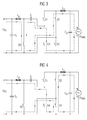
- the Fig. 3 first explains the switch-on of the switching sequence in the positive half cycle in accordance with the inverter according to the invention Fig. 1 , wherein the energy flow from the DC voltage part takes place in the AC voltage part.
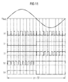
- the control of the switching elements and in particular their timing can thereby Fig. 11 be removed.
- the switching elements S2 and S4 Like from the Fig. 11 can be seen, remain to generate the positive half-wave at the output terminals of the AC voltage part, the switching elements S2 and S4 always closed while the switching element S1 always remains off.
- the switching element S5 is closed, and the switching element S3, which is also referred to as a clock switch in this context, is open (FIG. Fig. 3 ).
- the switching element S5 is opened, and the switching element S3 is closed ( Fig. 4 ).
- the positive side of the charging capacitor C is grounded, whereby it discharges through the AC-side inductance L S , and thereby at the load U net , as in the Fig. 3 Obviously, a positive voltage is generated.
- the charging capacitor C 0 is at the positive potential of the DC voltage source U IN , whereby it is recharged.
- the AC-side inductance L S drives the load current, and in turn provides a positive voltage at the load U- net .
- the duty cycle is, as from the Fig.
- the switch-on phase of the switching element S5 is always longer, and the switch-on phase of the switching element S3 is correspondingly shorter and shorter until the maximum of the positive half wave at the load U network is reached. Thereafter, the switch-on of the switching element S5 is always selected to be shorter, and the switch-on of the switching element S3 accordingly longer and longer, until the zero crossing of the positive half-wave is reached at the load U-network.
- the generation of the negative half wave is in the Fig. 5 and Fig. 6 shown.
- the switching elements S1 and S3 always remain closed while the switching element S4 always remains open.
- the switching element S5 is closed, and the switching element S2, which is now referred to as a clock switch in this context, is open ( Fig. 5 ).
- the switching element S5 is opened, and the switching element S2 is closed ( Fig. 6 ).
- the positive side of the charging capacitor C is in turn grounded, whereby it discharges via the AC-side inductance L s , but it at the load U net , as in the Fig.
- a polarity reversal of the voltage Fig. 3 causes.
- the charging capacitor C 0 is at the positive potential of the DC voltage source U IN , whereby it is recharged.
- the AC-side inductance L S drives the load current, and in turn provides a reverse polarity at the load U- net .
- the duty cycle is, as from the Fig. 11 It can be seen that the switch-on phase of the switching element S5 is always longer, and the switch-on phase of the switching element S2 is correspondingly shorter and shorter until the minimum of the negative half-wave at the load U network is reached. Thereafter, the switch-on of the switching element S5 is always selected to be shorter, and the switch-on of the switching element S2 correspondingly longer and longer, until the zero crossing of the negative half-wave is reached at the load U net .
- the inverter according to the invention can be operated bidirectionally, as based on Fig. 7 to 10 is explained. Thus, it is also suitable for the recovery of energy from the AC voltage part in the DC part.
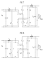
- the Fig. 7 first explains the switch-on of the switching sequence in the positive half cycle in accordance with the inverter according to the invention Fig. 1 , wherein the energy flow is now made from the AC voltage part in the DC part.
- the control of the switching elements and in particular their timing can thereby Fig. 12 be removed.
- the switching elements S2 and S4 now always remain closed at the positive half-wave at the input terminals of the AC voltage part, while the switching element S1 always remains switched off.
- the switching element S3 is closed, and the switching element S5, which now referred to as a clock switch in this context is, is open ( Fig. 7 ).
- the switching element S3 is opened, and the switching element S5 is closed ( Fig. 8 ).
- the positive side of the charging capacitor C is at the positive output terminal of the DC voltage part, whereby it discharges via the DC-side inductance L P , and thereby backs up a positive voltage.
- the charging capacitor C is recharged by the positive half-wave at the input terminals of the AC voltage part.
- the DC-side inductance L P drives the load current, and provides with respect to the Fig. 8 upper output terminal of the DC part in turn for a positive voltage.
- the duty cycle is, as from the Fig.
- the switch-on phase of the switching element S5 is always longer, and the switch-on phase of the switching element S3 is correspondingly shorter and shorter until the maximum of the positive half-wave at the input terminals of the Wchselnapssteils is reached. Thereafter, the switch-on of the switching element S5 is always selected to be shorter, and the switch-on of the switching element S3 correspondingly longer and longer, until the zero crossing of the positive half-wave is reached.
- the generation of the negative half wave is in the FIGS. 9 and 10 shown.
- the switching elements S1 and S3 always remain closed while the switching element S4 always remains open.
- the switching element S2 is closed, and the switching element S5, which in turn is referred to as a clock switch in this context, is open (FIG. Fig. 9 ).
- the switching element S2 is open, and the switching element S5 is closed ( Fig. 10 ).
- the positive side of the charging capacitor C is at the positive output terminal of the DC voltage part, whereby it discharges via the DC-side inductance L P , and thereby a positive Restores voltage.
- the turn-off phase of the charging capacitor C is due to the driving of the switching elements of the bridge circuit according to Fig. 10 also so charged by the negative half-wave at the input terminals of the AC voltage part, that at the in relation to the Fig. 10 left side of the charging capacitor C is a positive charge.
- the DC-side inductance L P drives the load current, and provides with respect to the Fig. 10 upper output terminal of the DC part in turn for a positive voltage.
- the duty cycle is, as from the Fig. 12 it can be seen that the switching-on phase of the switching element S5 is getting longer and longer, and the switch-on phase of the switching element S2 becomes shorter and shorter until the minimum of the negative half-wave at the input terminals of the AC voltage part is reached. Thereafter, the switch-on of the switching element S5 is always selected to be shorter, and the switch-on of the switching element S2 correspondingly longer and longer, until the zero crossing of the negative half-wave is reached.
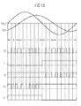
- Fig. 13 is the time course of voltage, current and control signal for the switching elements S1, S2, S3, S4 and S5 at reactive power consumption with inductive load and inverter according to the invention Fig. 1 shown as it is given in island operation.
- the time course is shown with an inductive load in stand-alone operation, the mains current runs after the grid voltage accordingly. This results in a mixed operation between feeding into the grid and feeding back reactive energy from the power grid.
- a voltage half wave there are both negative and positive current characteristics. Accordingly, those in the Fig.
- the switching states of the first switching element S1 and the fourth switching element S4 correspond to those in FIG Fig. 11 shown.
- the third switching element S3 and during a negative half cycle the second switching element S2 inverse clockwise to the fifth switching element S5. If the signs of the mains current and the mains voltage are equal, a switching cycle begins with the switching on of the fifth switching element S5 (supply). On the other hand, with different signs, a switching cycle begins with the switching on of the third switching element S3 during a positive voltage half-cycle, and with the switching on of the second switching element S2 during a negative voltage half-cycle.
- Fig. 14 the time profiles are shown for an island operation with capacitive load.
- the mains current precedes the mains voltage.
- Fig. 13 shown switching signal waveforms change so that the ratios of the turn-on to the turn-off of the clocking switching elements S5, S3 and S2.
- the Fig. 15 shows the basic circuit diagram of a second embodiment of the inverter according to the invention with ZETA converter, which can also be understood as a grid-guided inverter.
- the inverter according to Fig. 15 also has a bridge circuit with four switching elements S1, S2, S3 and S4, in which two opposite terminals 1, 2 of the bridge circuit are connected to the DC part of the inverter, and the other two terminals 3, 4 of the bridge circuit to the AC voltage part of the inverter ,
- the actual conversion of DC voltage into AC voltage is again via the four switching elements S1, S2, S3 and S4 in the bridge circuit, which represents a full bridge, wherein in in itself known manner by suitable control of the switching elements S1, S2, S3 and S4 DC and AC voltage are interconvertible.
- an AC-side inductance L S is switched.
- a DC-side switching element S5 is coupled to the positive DC terminal, which is followed by a switched between the DC side switching element S5 and the bridge circuit in series charge capacitor C, wherein in the series connection between the DC side switching element S5 and the charging capacitor C on the one hand, and the negative DC terminal on the other hand, a DC-side inductance L P is connected, which connects the side of the charging capacitor C connected to the positive DC voltage terminal to the negative DC voltage terminal.
- the DC voltage source U IN which also serves as a storage element in an energy flow from the AC voltage part in the DC part.
- the load U network which also acts as a source in an energy flow from the AC voltage part in the DC part.
- an AC-side smoothing capacitor C 0 is connected, and in the DC voltage part, a DC-side smoothing capacitor C i .
- the switching elements S1, S2, S3, S4 and S5 are preferably semiconductor switching elements, in particular a power MOSFET or IGBT.
- the Fig. 16 shows the embodiment according to Fig. 15 with additional discharge diodes on the respective switching elements S1, S2, S3, S4 and S5.
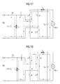
- the Fig. 17 first explains the switch-on of the switching sequence in the positive half cycle in accordance with the inverter according to the invention Fig. 15 , wherein the energy flow from the DC voltage part takes place in the AC voltage part.
- the control of the switching elements and in particular their timing can thereby Fig. 25 be removed.
- the switching elements S1 and S3 always remain closed to generate the positive half wave at the output terminals of the AC voltage part, while the switching element S4 always remains open.
- the switching element S5 is closed, and the switching element S2, which is also referred to as a clock switch in this context, is open (FIG. Fig. 17 ).
- the switching element S5 is opened, and the switching element S2 is closed ( Fig. 18 ).
- the switch-on is the, in relation to the Fig. 17 seen, left side of the charging capacitor C at the positive potential of the DC voltage source U IN , and discharges via the AC-side inductance L S. It is connected to the load U net , as in the Fig. 17 Obviously, a positive voltage is generated.
- the charging capacitor C 0 is disconnected from the positive potential of the DC voltage source U IN .
- the AC-side inductance L S drives the load current, and in turn provides a positive voltage at the load U- net .
- the duty cycle is, as from the Fig. 25 can be seen, so chosen that the switch-on of the switching element S5 is getting longer, and the switch-on of the switching element S2 correspondingly shorter and shorter until the maximum of the positive half-wave at the load U net is reached. Thereafter, the switch-on of the switching element S5 is always selected shorter, and the switch-on of the switching element S2 correspondingly longer and longer, until the zero crossing of the positive half-wave is reached at the load U net .
- the generation of the negative half wave is in the FIGS. 19 and 20 shown.
- the switching elements S2 and S4 always remain closed, while the switching element S1 always remains open.
- the switching element S5 is closed, and the switching element S3, which is now referred to as a clock switch in this context, is open (FIG. Fig. 19 ).
- the switching element S5 is opened, and the switching element S3 is closed ( Fig. 20 ). This results in the in the FIGS. 19 and 20 drawn energy flow.
- the switch-on is the, in relation to the Fig.
- the switch-on of the switching element S5 is getting longer, and the switch-on of the switching element S3 correspondingly shorter and shorter until the minimum of the negative half-wave at the load U net is reached. Thereafter, the switch-on of the switching element S5 is always selected to be shorter, and the switch-on of the switching element S3 accordingly longer and longer, until the zero crossing of the negative half-wave is reached at the load U net .
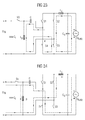
- This embodiment of the inverter according to the invention can be operated bidirectionally, as with reference to Fig. 21 to 24 is explained. Thus, it is also suitable for feeding back of energy from the AC voltage part in the DC part.
- the Fig. 21 first explains the switch-on of the switching sequence in the positive half cycle in accordance with the inverter according to the invention Fig. 15 , wherein the energy flow is now made from the AC voltage part in the DC part.
- the control of the switching elements and in particular their timing can thereby Fig. 26 be removed.
- the switching elements S1 and S3 now remain closed at the positive half-wave at the input terminals of the AC voltage part, while the switching element S4 always remains open.
- the switching element S2 is closed, and the switching element S5, which is now referred to as a clock switch in this context, is open (FIG. Fig. 21 ).
- the switching element S2 is open, and the switching element S5 is closed ( Fig. 22 ).
- the switch-on is the, in relation to the Fig. 21 seen right side of the charging capacitor C at positive potential, and discharges via the DC side inductance L P.
- the charging capacitor C is recharged by the positive half-wave at the input terminals of the AC voltage part.
- the DC-side inductance L P drives the load current, and provides with respect to the Fig. 22 upper output terminal of the DC voltage part for a positive voltage.
- the duty cycle is, as from the Fig.
- the switch-on phase of the switching element S5 is getting longer and longer, and the switch-on phase of the switching element S2 is correspondingly shorter and shorter until the maximum of the positive half-wave at the input terminals of the Wchselnapssteils is reached. Thereafter, the switch-on of the switching element S5 is always selected to be shorter, and the switch-on of the switching element S2 correspondingly longer and longer, until the zero crossing of the positive half-wave is reached.
- the generation of the negative half wave is in the FIGS. 23 and 24 shown.
- the switching elements S2 and S4 always remain closed, while the switching element S1 always remains open.
- the switching element S3 is closed, and the switching element S5, which in turn is referred to as a clock switch in this context, is open (FIG. Fig. 23 ).
- the switching element S3 is opened, and the switching element S5 is closed ( Fig. 24 ). This results in the in the FIGS. 23 and 24 drawn energy flow.
- the switch-on is the, in relation to the Fig. 23 seen right side of the charging capacitor C at positive potential, and discharges via the DC side inductance L P.
- the charging capacitor C is recharged by the positive half-wave at the input terminals of the AC voltage part.
- the DC side inductance L P drives the load current, and in turn provides the same with respect to Fig. 24 upper output terminal of the DC voltage part for a positive voltage.
- the duty cycle is, as from the Fig. 26 can be seen, so selected that the turn-on of the switching element S5 is getting longer, and the turn-on of the switching element S3 correspondingly shorter and shorter until the minimum of the negative half-wave is reached at the input terminals of the AC voltage part. Thereafter, the switch-on of the switching element S5 is always selected to be shorter, and the switch-on of the switching element S3 correspondingly longer and longer, until the zero crossing of the negative half-wave is reached.
- Fig. 27 is the time course of voltage, current and control signal for the switching elements S1, S2, S3, S4 and S5 at reactive power consumption with inductive load and inverter according to the invention Fig. 15 shown as it is given in island operation.
- Fig. 27 is the time course of voltage, current and control signal for the switching elements S1, S2, S3, S4 and S5 at reactive power consumption with inductive load and inverter according to the invention Fig. 1 shown as it is given in island operation.
- the time history is shown with an inductive load in isolated mode, the mains current runs after the mains voltage accordingly. This results in a mixed operation between feeding into the grid and feeding back reactive energy from the power grid.
- a voltage half wave there are both negative and positive current characteristics. Accordingly, those in the Fig.
- the switching states of the first switching element S1 and the fourth switching element S4 correspond to those in the Fig. 11 shown.
- the third switching element S3, and during a negative half cycle the second switching element S2 inverse clockwise to the fifth switching element S5. If the signs of the mains current and the mains voltage are equal, a switching cycle begins with the switching on of the fifth switching element S5 (supply). On the other hand, with different signs, a switching cycle begins with the switching on of the third switching element S3 during a positive voltage half-cycle, and with the switching on of the second switching element S2 during a negative voltage half-cycle.
- Fig. 28 the time profiles are shown for an island operation with capacitive load.
- the mains current precedes the mains voltage.
- Fig. 13 shown switching signal waveforms change so that the ratios of the turn-on to the turn-off of the clocking switching elements S5, S3 and S2.
Landscapes
- Engineering & Computer Science (AREA)
- Power Engineering (AREA)
- Inverter Devices (AREA)
Applications Claiming Priority (1)
| Application Number | Priority Date | Filing Date | Title |
|---|---|---|---|
| AT1092007A AT504777B1 (de) | 2007-01-23 | 2007-01-23 | Wechselrichter |
Publications (2)
| Publication Number | Publication Date |
|---|---|
| EP1950876A2 true EP1950876A2 (fr) | 2008-07-30 |
| EP1950876A3 EP1950876A3 (fr) | 2016-08-24 |
Family
ID=39365808
Family Applications (1)
| Application Number | Title | Priority Date | Filing Date |
|---|---|---|---|
| EP07122445.5A Withdrawn EP1950876A3 (fr) | 2007-01-23 | 2007-12-06 | Onduleur |
Country Status (2)
| Country | Link |
|---|---|
| EP (1) | EP1950876A3 (fr) |
| AT (1) | AT504777B1 (fr) |
Families Citing this family (1)
| Publication number | Priority date | Publication date | Assignee | Title |
|---|---|---|---|---|
| DE102018214497B4 (de) | 2018-08-28 | 2021-09-30 | Continental Automotive Gmbh | Wandlerschaltung zum Erzeugen einer Wechselspannung aus einer Gleichspannung sowie schaltbare Verglasung und ein Kraftfahrzeug |
Family Cites Families (1)
| Publication number | Priority date | Publication date | Assignee | Title |
|---|---|---|---|---|
| JP4524420B2 (ja) * | 2004-07-12 | 2010-08-18 | シーメンス アクチエンゲゼルシヤフト | インバータの駆動方法およびこの方法に適するインバータ |
-
2007
- 2007-01-23 AT AT1092007A patent/AT504777B1/de not_active IP Right Cessation
- 2007-12-06 EP EP07122445.5A patent/EP1950876A3/fr not_active Withdrawn
Also Published As
| Publication number | Publication date |
|---|---|
| AT504777A1 (de) | 2008-08-15 |
| AT504777B1 (de) | 2011-01-15 |
| EP1950876A3 (fr) | 2016-08-24 |
Similar Documents
| Publication | Publication Date | Title |
|---|---|---|
| EP2290797B1 (fr) | Procédé pour convertir une tension continue d'une source de tension continue, en particulier d'une source de tension continue PHOTOVOLTAIQUE, en une tension alternative | |
| DE102006010694B4 (de) | Wechselrichterschaltung für erweiterten Eingangsspannungsbereich | |
| DE102006025975B4 (de) | Wechselrichterschaltung und Verfahren zum Betreiben der Wechselrichterschaltung | |
| AT505801B1 (de) | Verfahren zum betrieb eines elektronisch gesteuerten wechselrichters | |
| EP2863528B1 (fr) | Utilisation d'un onduleur comme un convertisseur CC/CC | |
| DE102013212682B4 (de) | Energiespeichereinrichtung mit Gleichspannungsversorgungsschaltung und Verfahren zum Bereitstellen einer Gleichspannung aus einer Energiespeichereinrichtung | |
| EP2309639A1 (fr) | Onduleur capable de puissance réactive | |
| DE102014103454A1 (de) | System und Verfahren für einen Schaltleistungswandler | |
| EP2030299A1 (fr) | Onduleur destiné à injecter de l'énergie électrique dans un réseau de distribution d'énergie | |
| EP2709257A2 (fr) | Circuit de convertisseur de courant et procédé de commande du circuit de convertisseur de courant | |
| AT504944B1 (de) | Wechselrichter | |
| WO2019015920A1 (fr) | Convertisseur électrique à couplage galvanique | |
| EP3123603B1 (fr) | Procédé de modulation du fonctionnement en mode élévateur d'un convertisseur push-pull | |
| DE102011116593B4 (de) | Wechselrichter mit asymmetrischen Drosseln und einer Steuereinheit zum asymmetrischen Betrieb der Drosseln | |
| DE102012202867A1 (de) | Ladeschaltung für eine Energiespeichereinrichtung und Verfahren zum Laden einer Energiespeichereinrichtung | |
| EP2421135B1 (fr) | Onduleur sans transformateur avec convertisseur abaisseur | |
| WO2015062900A1 (fr) | Circuit de charge pour dispositif d'accumulation d'énergie et procédé permettant de charger un dispositif d'accumulation d'énergie | |
| CH700030B1 (de) | Schaltungsanordnung mit Wechselrichter- und Gleichstromstellerfunktion. | |
| EP3529102B1 (fr) | Convertisseur continu-continu et procédé pour opérer un convertisseur continu-continu | |
| EP1766767B1 (fr) | Procede d'utilisation d'un onduleur et dispositif de mise en oeuvre de ce procede | |
| DE102014203404A1 (de) | Stromrichterschaltung und Verfahren zum Betreiben derselben | |
| DE102013212692A1 (de) | Energiespeichereinrichtung mit Gleichspannungsversorgungsschaltung | |
| EP3571758A1 (fr) | Onduleur modulaire | |
| AT504777B1 (de) | Wechselrichter | |
| DE102014012028A1 (de) | Vorrichtung und ein Verfahren zum Laden oder Entladen eines elektrischen Energiespeichers mit beliebigen Betriebsspannungen |
Legal Events
| Date | Code | Title | Description |
|---|---|---|---|
| PUAI | Public reference made under article 153(3) epc to a published international application that has entered the european phase |
Free format text: ORIGINAL CODE: 0009012 |
|
| AK | Designated contracting states |
Kind code of ref document: A2 Designated state(s): AT BE BG CH CY CZ DE DK EE ES FI FR GB GR HU IE IS IT LI LT LU LV MC MT NL PL PT RO SE SI SK TR |
|
| AX | Request for extension of the european patent |
Extension state: AL BA HR MK RS |
|
| RAP1 | Party data changed (applicant data changed or rights of an application transferred) |
Owner name: SIEMENS AKTIENGESELLSCHAFT |
|
| RAP1 | Party data changed (applicant data changed or rights of an application transferred) |
Owner name: SIEMENS AKTIENGESELLSCHAFT |
|
| PUAL | Search report despatched |
Free format text: ORIGINAL CODE: 0009013 |
|
| AK | Designated contracting states |
Kind code of ref document: A3 Designated state(s): AT BE BG CH CY CZ DE DK EE ES FI FR GB GR HU IE IS IT LI LT LU LV MC MT NL PL PT RO SE SI SK TR |
|
| AX | Request for extension of the european patent |
Extension state: AL BA HR MK RS |
|
| RIC1 | Information provided on ipc code assigned before grant |
Ipc: H02M 7/537 20060101AFI20160721BHEP |
|
| STAA | Information on the status of an ep patent application or granted ep patent |
Free format text: STATUS: THE APPLICATION HAS BEEN PUBLISHED |
|
| AKY | No designation fees paid | ||
| AXX | Extension fees paid |
Extension state: RS Extension state: BA Extension state: AL Extension state: HR Extension state: MK |
|
| REG | Reference to a national code |
Ref country code: DE Ref legal event code: R108 |
|
| STAA | Information on the status of an ep patent application or granted ep patent |
Free format text: STATUS: THE APPLICATION IS DEEMED TO BE WITHDRAWN |
|
| 18D | Application deemed to be withdrawn |
Effective date: 20170225 |