EP1951012B1 - Procédé de fabrication d'une carte de circuit en utilisant un électro-placage - Google Patents
Procédé de fabrication d'une carte de circuit en utilisant un électro-placage Download PDFInfo
- Publication number
- EP1951012B1 EP1951012B1 EP08007710A EP08007710A EP1951012B1 EP 1951012 B1 EP1951012 B1 EP 1951012B1 EP 08007710 A EP08007710 A EP 08007710A EP 08007710 A EP08007710 A EP 08007710A EP 1951012 B1 EP1951012 B1 EP 1951012B1
- Authority
- EP
- European Patent Office
- Prior art keywords
- wiring
- plating layer
- plating
- pattern
- wiring board
- Prior art date
- Legal status (The legal status is an assumption and is not a legal conclusion. Google has not performed a legal analysis and makes no representation as to the accuracy of the status listed.)
- Ceased
Links
Images





Classifications
-
- H—ELECTRICITY
- H05—ELECTRIC TECHNIQUES NOT OTHERWISE PROVIDED FOR
- H05K—PRINTED CIRCUITS; CASINGS OR CONSTRUCTIONAL DETAILS OF ELECTRIC APPARATUS; MANUFACTURE OF ASSEMBLAGES OF ELECTRICAL COMPONENTS
- H05K3/00—Apparatus or processes for manufacturing printed circuits
- H05K3/10—Apparatus or processes for manufacturing printed circuits in which conductive material is applied to the insulating support in such a manner as to form the desired conductive pattern
- H05K3/18—Apparatus or processes for manufacturing printed circuits in which conductive material is applied to the insulating support in such a manner as to form the desired conductive pattern using precipitation techniques to apply the conductive material
-
- H—ELECTRICITY
- H05—ELECTRIC TECHNIQUES NOT OTHERWISE PROVIDED FOR
- H05K—PRINTED CIRCUITS; CASINGS OR CONSTRUCTIONAL DETAILS OF ELECTRIC APPARATUS; MANUFACTURE OF ASSEMBLAGES OF ELECTRICAL COMPONENTS
- H05K3/00—Apparatus or processes for manufacturing printed circuits
- H05K3/22—Secondary treatment of printed circuits
- H05K3/24—Reinforcing of the conductive pattern
- H05K3/243—Reinforcing of the conductive pattern characterised by selective plating, e.g. for finish plating of pads
-
- H—ELECTRICITY
- H05—ELECTRIC TECHNIQUES NOT OTHERWISE PROVIDED FOR
- H05K—PRINTED CIRCUITS; CASINGS OR CONSTRUCTIONAL DETAILS OF ELECTRIC APPARATUS; MANUFACTURE OF ASSEMBLAGES OF ELECTRICAL COMPONENTS
- H05K2203/00—Indexing scheme relating to apparatus or processes for manufacturing printed circuits covered by H05K3/00
- H05K2203/03—Metal processing
- H05K2203/0361—Stripping a part of an upper metal layer to expose a lower metal layer, e.g. by etching or using a laser
-
- H—ELECTRICITY
- H05—ELECTRIC TECHNIQUES NOT OTHERWISE PROVIDED FOR
- H05K—PRINTED CIRCUITS; CASINGS OR CONSTRUCTIONAL DETAILS OF ELECTRIC APPARATUS; MANUFACTURE OF ASSEMBLAGES OF ELECTRICAL COMPONENTS
- H05K2203/00—Indexing scheme relating to apparatus or processes for manufacturing printed circuits covered by H05K3/00
- H05K2203/05—Patterning and lithography; Masks; Details of resist
- H05K2203/0502—Patterning and lithography
- H05K2203/0542—Continuous temporary metal layer over metal pattern
-
- H—ELECTRICITY
- H05—ELECTRIC TECHNIQUES NOT OTHERWISE PROVIDED FOR
- H05K—PRINTED CIRCUITS; CASINGS OR CONSTRUCTIONAL DETAILS OF ELECTRIC APPARATUS; MANUFACTURE OF ASSEMBLAGES OF ELECTRICAL COMPONENTS
- H05K3/00—Apparatus or processes for manufacturing printed circuits
- H05K3/0011—Working of insulating substrates or insulating layers
- H05K3/0044—Mechanical working of the substrate, e.g. drilling or punching
- H05K3/0052—Depaneling, i.e. dividing a panel into circuit boards; Working of the edges of circuit boards
-
- H—ELECTRICITY
- H05—ELECTRIC TECHNIQUES NOT OTHERWISE PROVIDED FOR
- H05K—PRINTED CIRCUITS; CASINGS OR CONSTRUCTIONAL DETAILS OF ELECTRIC APPARATUS; MANUFACTURE OF ASSEMBLAGES OF ELECTRICAL COMPONENTS
- H05K3/00—Apparatus or processes for manufacturing printed circuits
- H05K3/10—Apparatus or processes for manufacturing printed circuits in which conductive material is applied to the insulating support in such a manner as to form the desired conductive pattern
- H05K3/108—Apparatus or processes for manufacturing printed circuits in which conductive material is applied to the insulating support in such a manner as to form the desired conductive pattern by semi-additive methods; masks therefor
-
- H—ELECTRICITY
- H05—ELECTRIC TECHNIQUES NOT OTHERWISE PROVIDED FOR
- H05K—PRINTED CIRCUITS; CASINGS OR CONSTRUCTIONAL DETAILS OF ELECTRIC APPARATUS; MANUFACTURE OF ASSEMBLAGES OF ELECTRICAL COMPONENTS
- H05K3/00—Apparatus or processes for manufacturing printed circuits
- H05K3/40—Forming printed elements for providing electric connections to or between printed circuits
- H05K3/42—Plated through-holes or plated via connections
- H05K3/425—Plated through-holes or plated via connections characterised by the sequence of steps for plating the through-holes or via connections in relation to the conductive pattern
- H05K3/426—Plated through-holes or plated via connections characterised by the sequence of steps for plating the through-holes or via connections in relation to the conductive pattern initial plating of through-holes in substrates without metal
-
- H—ELECTRICITY
- H05—ELECTRIC TECHNIQUES NOT OTHERWISE PROVIDED FOR
- H05K—PRINTED CIRCUITS; CASINGS OR CONSTRUCTIONAL DETAILS OF ELECTRIC APPARATUS; MANUFACTURE OF ASSEMBLAGES OF ELECTRICAL COMPONENTS
- H05K3/00—Apparatus or processes for manufacturing printed circuits
- H05K3/40—Forming printed elements for providing electric connections to or between printed circuits
- H05K3/42—Plated through-holes or plated via connections
- H05K3/425—Plated through-holes or plated via connections characterised by the sequence of steps for plating the through-holes or via connections in relation to the conductive pattern
- H05K3/427—Plated through-holes or plated via connections characterised by the sequence of steps for plating the through-holes or via connections in relation to the conductive pattern initial plating of through-holes in metal-clad substrates
Definitions
- the present invention relates to a method of manufacturing a wiring board used for a semiconductor device. More particularly, the present invention relates to a method of manufacturing a wiring board on which wiring, used for feeding electricity to conduct plating, is not required as it would be in the case where the wiring board is manufactured by utilizing electro plating.
- a wiring board used for a semiconductor device for example, a large-sized board 1 made of resin, such as glass prepreg shown in Fig. 1A , is prepared. After matrix-shaped wiring patterns 5, corresponding to those for a plurality of wiring boards 3, have been simultaneously formed, the large-sized board 1 is cut along the predetermined cutting lines 7. In this way, individual wiring boards 3 are obtained.
- Fig. 1B is an enlarged view of the wiring pattern 5 and the plating wiring 9 shown in Fig. 1A .
- Reference numeral 11 is a bonding pad
- reference numeral 13 is a through-hole.
- the large-sized board 1 is dipped in a plating solution (not shown), and the electrode (not shown) for plating is connected to the plating wiring 9 provided on the outer circumference of the large-sized board 1.
- the wiring pattern 5 is fed with electricity, so that electro plating of nickel or gold can be conducted in the necessary portion on the wiring pattern 5.
- the large-sized board 1 is cut in a portion on the inside (a portion along the cutting line 7 shown by a broken line) of the plating wiring 9, and the individual wiring boards 3 are obtained. Therefore, on the wiring pattern 5 of the wiring board 3, the portion 15, which is necessary only for connecting with the plating wiring 9 and not necessary for transmitting an electric signal, exists from the through-hole 11 to the outer periphery of the wiring board 3.
- a wiring board As an example of the wiring board 3 described above, there is a wiring board, referred to as "BGA (Ball Grid Array)", used for a semiconductor device.
- BGA Bit Grid Array
- FIG. 4A is a view showing BGA in which the thus manufactured wiring board 3 is used.
- a method of manufacturing a wiring pattern forming method of the cross-sectional portion which is indicated by reference mark X in Fig. 4A , is shown.
- Fig. 2A first of all, the large laminated plate 10, both sides of which are covered with copper, which is made when pieces of copper foil 17, 17 are laminated on both sides of the resin board (glass prepreg board) 1, is prepared. On this large laminated plate 10, both sides of which are covered with copper, a plurality of wiring boards 3 shown in Fig. 1A are formed.
- through-holes 13 are formed at predetermined positions with a drill (not shown).
- the electroless plating layer 19 of copper is formed on all surfaces including the inner wall of the through-hole 13.
- a film-shaped etching resist which is referred to as a dry resist film, is laminated. Exposure and development are conducted on the dry resist film, so that the resist pattern 23 corresponding to a predetermined wiring pattern can be formed.
- etching is conducted while the resist pattern 23 is being used as a mask, and the electrolytic copper plating layer 21, the electroless copper plating layer 19 and the copper foil 17, which are exposed from the resist pattern 23 and unnecessary for forming the wiring pattern, are removed so as to form the wiring pattern 5.
- Fig. 2G the resist pattern 23 is removed. Due to this removal of the resist pattern 23, the wiring pattern 5 is exposed.
- This wiring pattern 5 is connected to the plating wiring 9 ( Figs. 1 and 2 ), which is formed simultaneously with the wiring pattern 5, via the connecting portion 5c of the wiring pattern 5.
- the wiring pattern 5 and the plating wiring 9 are connected to each other as shown in Fig. 1 .
- this plating wiring 9 is formed on the large resin board 1 into a frame shape outside the cutting line 7 for obtaining a plurality of wiring boards 3. Before cutting, this plating wiring 9 is connected to the wiring patterns 5 of all of the plurality of wiring boards 3.
- solder resist is coated by printing, and the solder resist pattern 25 is formed by means of exposure and development. At this time, the solder resist pattern 25 is formed so that the predetermined portions such as a bonding pad 11 of the wiring pattern 5 and a pad (a joining portion of the solder ball) 31 for connecting with the outside can be exposed.
- Fig. 3B electricity is fed through the plating wiring 9 ( Fig. 1 ), and the electrolytic nickel plating 27 is conducted on the wire boding pad 11 and the pad 31 for connecting with the outside. Next, the electrolytic gold plating 29 is conducted.
- Fig. 3C is a view obtained when Fig. 3B is viewed from top. However, the solder resist 25 is omitted in Fig. 3C .
- the wiring pattern 5 is short-circuited by the plating wiring 9.
- Fig. 3D the large-sized board 1 is cut on the cutting lines 7 shown in Figs. 3B and 3C , so that the individual wiring boards 3 can be obtained.
- Fig. 4B is a view obtained when the wiring board indicated by reference mark X in Fig. 4A is viewed from top, wherein the sealing resin 37 and the solder resist 25 are omitted in Fig. 4B .
- the official gazette of JP-A-2000-114412 discloses the prior art relating to the present invention.
- the wiring pattern and the board are closely contacted with each other and further the wiring pattern is made fine and furthermore the solder resist and the conductor portion are closely contacted with each other. Therefore, when electro plating is conducted while a copper layer formed on the board face is being used as an electricity feeding layer and when the copper layer is etched while the resist pattern is being used as a mask, the wiring pattern is formed.
- the wiring board manufactured by the conventional subtractive method described above due to the necessity of feeding electricity for conducting electro plating, an unnecessary portion is generated on the wiring pattern. By this unnecessary portion, a signal is reflected and noise is generated. Therefore, the electrical characteristic of the semiconductor device is deteriorated, and further an arrangement of the wiring pattern is restricted. Accordingly, it becomes difficult to arrange the wiring pattern 5 with high density.
- US 3,742,597 discloses a manufacturing method for a printed circuit board. Such method uses three screens which correspond to the final circuit, pad and contact location. In copper-clad boards holes are formed by drilling. Then a copper flashing is deposited on the board by an electroless process. The flash is also deposited on the surfaces of the insulation board defining the holes during this operation. A screen having spattered portions corresponding to the holes through the board is registered with the board. After applying an electroplating resist on the board through the screen, a conventional electroplating operation deposits additional copper at the pads and through the holes. Then the exposed copper portions are cleaned before a succeeding electroplating process deposits solder onto the pads and through the holes. No other solder plates the board because the electroplating resist is still on the board.
- the board is cleaned completely. Now the board can be etched. A screen having spattered portions representing the wiring is registered with the printed circuit board. Then the etching resist is applied through the transparent portions, which correspond to the circuits and contacts. The board is also immersed in a conventional etching solution. All copper portions not coated with solder or resist are removed from the board. However, the copper etching solution cannot remove the circuit pads or contacts.
- US 4,289,575 discloses a method for etching predetermined portions of a wiring substrate having a copper wiring pattern disposed thereon.
- the copper wiring pattern comprises contact tabs and lands.
- the tabs are connected to the pad via electroplating leads and a circuit lead.
- the lands are interconnected through a circuit lead, whereas the lands are connected to an electroplating lead acting as an overlapping terminal.
- a first organic insulating film having a plating resistant property is selectively coated on the substrate, except for the contact regions on the desired portions of the electroplating leads.
- second films are coated on the lands and branch portions of the lead. The above portions of the first film are partially overlapped by the second films.
- Overlapping coating for example gold, silver or a double-layer plated coating of gold or nickel are formed on the exposed region of the copper pattern. Thereafter, the second films and are removed.
- an exemplary method of manufacturing a wiring board by utilizing electro plating comprising the following steps of: forming first electroless plating layers on both sides of an insulating substrate, both sides thereof being covered with metallic foils in advance; forming first electro plating layers on the first electroless plating layers by supplying an electric power from the first electroless plating layers; forming wiring patterns by removing predetermined portions of the first electro plating layers, the first electroless plating layers and the metallic foils; forming second electroless plating layers on the insulating substrate including the wiring patterns; forming a plating resist pattern so that a first predetermined portions of the wiring patterns are exposed; forming a second electro plating layer on the first predetermined portion of the wiring patterns by supplying an electric power from the second electroless plating layers; removing the plating resist pattern; removing the second electroless plating layers exposed from the second electro plating layer; and forming a solder resist pattern so that a predetermined portions including the first predetermined portion of the wiring patterns are exposed.
- the metallic foils, the first electroless plating layers and the first electro plating layers are copper.
- the wiring pattern forming step comprises the following sub-steps: coating the first electro plating layers with an etching resist; and forming an etching resist pattern by exposing and developing the etching resist; and etching to removing an area which is exposed from the etching resist pattern.
- the plating resist pattern forming step comprises the following sub-steps: coating all surfaces of the substrate including the wiring pattern with the plating resist pattern; and exposing and developing the plating resist so that the first predetermined portion of the wiring patterns is exposed.
- the method of manufacturing a wiring board further comprises the following step: forming a through-hole in the insulating substrate, both sides thereof being covered with metallic foils in advance, so that the first electroless plating layers are formed on both sides of the insulating substrate, as well as on an inner wall of the through-hole, and the first electro plating layers are formed on the first electroless plating layers.
- a method of manufacturing a wiring board by utilizing electro plating comprising the following steps in the following order: forming a first electroless plating layer on a surface of an insulating substrate; forming a first plating resist pattern on the first electroless plating layer; forming a first electro plating layer on the first electroless plating layer exposed from the first plating resist pattern by supplying an electric power from the first electroless plating layers, to define a wiring pattern; removing the first plating resist pattern; forming a second plating resist pattern so that a first predetermined portion of the wiring pattern is exposed; forming a second electro plating layer on a first predetermined portion of the wiring pattern by supplying an electric power from the first electroless plating layer; removing the second plating resist pattern; removing the first electroless plating layers exposed from the wiring pattern; and forming a solder resist pattern so that a predetermined portion including the first predetermined portion of the wiring patterns is exposed.
- an exemplary method of manufacturing a wiring board by utilizing electro plating comprising the following steps of: forming a first electroless plating layer on a surface of an insulating substrate; forming a first plating resist pattern on the first electroless plating layer; forming a first electro plating layer on the first electroless plating layer exposed from the first plating resist pattern by supplying an electric power from the first electroless plating layers, to define a wiring pattern; forming a second plating resist pattern so that a first predetermined portion of the wiring pattern is exposed; forming a second electro plating layer on a first predetermined portion of the wiring pattern by supplying an electric power from the first electroless plating layer; removing the first and second plating resist patterns; removing the first electroless plating layers exposed from the wiring pattern; and forming a solder resist pattern so that a predetermined portion including the first predetermined portion of the wiring patterns is exposed.
- the first electroless plating layers and the first electro plating layers are copper.
- the first plating resist pattern forming step comprises the following sub-steps of: coating the first electroless plating layer with a plating resist, and exposing and developing the plating resist; and the second plating resist pattern forming step comprises the following sub-steps of: coating the surface of the substrate including the wiring pattern with a plating resist, and exposing and developing the plating resist.
- the method of manufacturing a wiring board further comprises the following step: forming a through-hole in the insulating substrate, so that the first electroless plating layer is formed on the surface of the insulating substrate, as well as on an inner wall of the through-hole, and the first plating resist pattern is formed on the first electroless plating layer.
- One surface or the respective surfaces of the insulating substrate are coated with a copper foil in advance, the first electroless plating layer is formed on the copper foil and the copper foil is simultaneously removed at the step of removing the first electroless plating layer exposed from the wiring pattern.
- the solder resist pattern forming step comprises the following sub-steps of: coating the surface of the substrate with a solder resist; and exposing and developing the solder resist to expose a predetermined portion including the first predetermined portion of the wiring pattern.
- the first predetermined portion of the wiring pattern which is exposed from the solder resist includes areas for wire-bonding pad or external connecting terminal pad.
- the second electro plating layer formed on the first predetermined portion includes an electrolytic nickel plated layer and an electrolytic gold plated layer formed on the nickel plated layer.
- the wiring board is individually obtained by cutting a large-sized substrate along cutting lines; the first electro plating layer forming step is carried out by supplying an electric power from the first electroless plating layers provided along a peripheral edge of the large-sized substrate; and wiring pattern forming step is carried out in such a manner that the wiring patterns do no extend to the cutting line at an edge of the individual wiring board.
- the present invention it becomes unnecessary to provide a plating wire for conducting electro plating. Therefore, the above problems, caused by the conventional subtractive method, are not caused.
- a resin board 1 it is possible to use a multiple layer wiring board, on which a plurality of wiring layers are formed. Further, the wiring pattern may be formed on both sides of the resin board 1. Furthermore, the wiring pattern may be formed only on one side of the resin board 1.
- FIG. 5A to 5F and Figs. 6A to 6C the manufacturing method of manufacturing a wiring board by the subtractive method exemplary will be explained below in the order of the manufacturing steps.
- a portion corresponding to the portion indicated by X of Fig. 4A is shown by an enlarged sectional view.
- the wiring pattern 5 is formed on the large-sized board 1.
- the plating wiring 9 shown in Fig. 1
- the portion 5c connected to the plating wiring 9, which are provided in the conventional steps 2E to 2G, are not formed, as shown in the corresponding Figs. 5A to 5C , respectively.
- a film-shaped etching resist layer which is referred to as a dry film resist, is laminated on the electrolytic copper plating layer 21, and then exposure and development are conducted on the dry film resist so as to form an etching resist pattern 23.
- a portion in the circumferential periphery of the board 1 corresponding to the connecting portion 5c (shown in Fig. 2G ) to the plating wiring 9 (shown in Fig. 1 ) is left as an exposed portion not covered with the etching resist pattern 23.
- etching is conducted, and the electrolytic copper plating layer 21, the electroless copper plating layer 19 and the copper foil layer 17, which are located in an unnecessary portion not covered with the resist pattern 23, are removed, so that the wiring pattern 5 can be formed.
- Fig. 5C the resist pattern 23 is removed. Due to this removal of the resist pattern 23, the wiring pattern 5 is exposed. As described before, on this wiring pattern 5, the connecting portion 5c (shown in Fig. 2G ) is not provided. Therefore, the wiring patterns are not connected. As described before, the plating wiring 9 (shown in Fig. 1 ), which is formed into a frame-shape outside the cutting line 7 to obtain a plurality of wiring boards 3 on the large resin board 1 in the conventional example, is not provided.
- a plating resist is coated so that the predetermined portions of the wiring pattern 5 such as a wire bonding pad region 5a and a pad 5b for the external connection terminal can be exposed, on which electrolytic nickel plating and electrolytic gold plating are conducted in the subsequent step. Then, the plating resist pattern (the plating mask) 43 is formed by conducting the steps of exposure and development.
- Fig. 6A electricity is fed by the electroless plating layer 41 so as to form the electrolytic nickel plating layer 27 and the electrolytic gold plating layer 29 on the wire bonding pad and others.
- the electroless copper plating layer 41 for feeding electricity extends to the outside of the individual wiring boards 3.
- the large-sized board is dipped in a plating solution (not shown), so that electricity can be fed while the electroless copper plating layer in the circumferential edge portion of the large-sized board is being used as an electrode.
- solder resist is coated, and exposure and development are conducted so as to form the resist pattern 45 from which the wire boding pad 5a and the pad 5b for the external connection are exposed.
- the large-sized board is cut off so as to obtain the individual wiring boards.
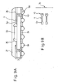
- the semiconductor element 33 is mounted on the thus obtained wiring board and then sealing is conducted with the resin 37 and the solder balls 39 are joined. In this way, the semiconductor device (BGA) shown in Fig. 9A is obtained.
- the semiconductor device (BGA) shown in Fig. 9A is obtained.
- Fig. 9B on this wiring board, no unnecessary portion is provided on the wiring pattern 5, that is, the plating wiring and the connecting portion to it are not provided. Therefore, the problems, which used to occur in the case of the conventional wiring board, do not occur.
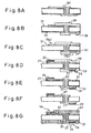
- Figs. 7A to 7F and Figs. 8A to 8G the method of manufacturing a wiring board by the semi-additive method relating to the present invention will be explained in the order of the manufacturing steps.
- a portion corresponding to the portion X of Fig. 4A is shown by an enlarged sectional view.
- the plating wiring 9 shown in Fig. 1
- the wiring board is manufactured by the following manufacturing steps.
- Fig. 7A the large resin board (glass prepreg) 1 is prepared.
- the through-hole 13 is formed with a drill.
- the electroless copper plating layer 51 is formed on all surface including the inner wall of the through-hole 13.
- the resist 53 is coated on the electroless copper plating layer 51.
- the plating resist is subjected to exposure and development so as to form the plating resist pattern 55 corresponding to the shape of the wiring pattern.
- this plating resist pattern 55 an end edge portion of the board 1 is left to be a portion covered with the plating resist pattern 55.
- Fig. 7F electricity is fed from the electroless plating layer 51, and a portion exposed from the plating resist pattern 55 is subjected to electrolytic copper plating so as to form the electrolytic copper plating layer 57. In this way, the wiring pattern is formed.
- electricity is fed to the electroless plating layer 51 by the electroless copper plating layer provided in the circumferential edge portion of the large-sized board.
- plating resist is coated so that the predetermined portions of the wiring pattern such as a wire bonding pad region 5a and a pad 5b for the external connection terminal can be exposed, on which electrolytic nickel plating and electrolytic gold plating are conducted. Then, the plating resist pattern (the plating mask) 59 is formed by conducting the steps of exposure and development.
- the electroless plating layer 51 which is exposed from the wiring pattern 57, is removed by means of quick etching of copper.
- an electric continuity portion such as a wiring pattern or an electroless plating layer does not exist in the end edge portion of each wiring board.
- solder resist is coated, and exposure and development are conducted so as to form the resist pattern 61 from which the wire boding pad 5a and the pad 5b for the external connection are exposed.
- the large-sized board is cut so as to obtain a plurality of the individual wiring boards.
- the semiconductor element is mounted on the thus obtained wiring board and then sealing is conducted with the resin 37 and the solder ball 39 is joined. In this way, the semiconductor device shown in Fig. 9A is obtained.
- Fig. 9B on this wiring board, no unnecessary portion, that is, the connecting portion to the plating wiring is not provided on the wiring pattern. Therefore, the problems, which used to occur in the case of the conventional wiring board, do not occur.
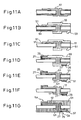
- Fig. 10 and 11 are views showing an exemplary manufacturing process of manufacturing a wiring board.
- a wiring pattern is formed on the resin board 1, on both sides of which the copper foil 17 is adhered, by the same method as that of the embodiment.
- the electroless plating layer 51 is formed on the resin board 1, on both sides of which the copper foil 17 is adhered, as shown in Figs. 10A, 10B and 10C .
- the copper foil 17 is simultaneously removed as shown in Figs. 11C and 11F .
- Other points are the same as those of the embodiment shown in Figs. 7A to 7F and 8A to 8G .
- Figs. 12A to 12E a further exemplary manufacturing method of manufacturing a wiring board will be explained below.
- the manufacturing steps are shown in Figs. 12A to 12E .
- electrolytic copper plating is conducted on a portion exposed from the plating resist pattern 55 so as to form the wiring pattern 57 (shown in Figs. 7F and 10F ), and after that, the resist pattern 55 is removed (shown in Figs. 8A and 11A ).
- manufacturing is conducted as follows. As shown in Fig.
- the resist pattern 55 is not removed, that is, the resist pattern 55 is left as it is, and plating resist is coated from the top of the resist pattern 55, and then the plating resist pattern (the plating mask) 59 is formed by means of exposure and development so that the portions, on which electrolytic nickel plating or electrolytic gold plating is conducted, such as a bonding pad region 5a and a pad region 5b for the external connection terminal can be exposed.
- Fig. 12B electricity is fed by the electroless plating layer 51, and the electrolytic nickel plating 27 and the electrolytic gold plating 29 are conducted on the predetermined portions on the wiring pattern 57 such as a wire bonding pad region 5a and a pad region 5b for the external connection terminal.
- electricity is fed to the electroless plating layer 51 by the circumferential edge portion of the large-sized board in the same manner as that described before.
- the electroless plating layer 51 which is exposed from the wiring pattern 57, is removed by means of quick etching of copper.
- electrically continuous portions such as a wiring pattern and an electroless plating layer do not exist in the end edge portion of each wiring board.
- solder resist is coated. Then the solder resist is exposed and developed to form the resist pattern 61 so that the wire bonding pad 5a and the pad 5b for external connection terminal can be exposed.
- the large-sized board is cut off so as to obtain the individual wiring boards.
- the semiconductor element 33 is mounted on the thus obtained wiring board and then sealing is conducted with the resin 37 and the solder ball 39 is joined. In this way, the semiconductor device is obtained.
- no unnecessary portion is provided on the wiring pattern, that is, the connecting portion to the plating wiring is not provided on the wiring pattern. Therefore, the problems, which used to occur in the case of the conventional wiring board, are not caused.
- the example illustrated in Figs. 12A to 12E relates to a case in which the resist pattern 55 is not removed in the process of the embodiment and the plating resist pattern (the plating mask) 59 is formed from the top of this resist pattern 55.
- the wiring board can be manufactured by the completely same process.
- Figs. 12A to 12E as described above, the resist pattern 55 is not removed. Therefore, in the electro plating step, for example, as shown in Figs. 8A to 8G or 11A to 11G , the electrolytic nickel plating layer 27 and the electrolytic gold plating layer 29 are not precipitated on the side of the bonding pad 5a but the electrolytic nickel plating layer 27 and the electrolytic gold plating layer 29 are precipitated only on the flat face.
- Figs. 13A and 13B models of the following two cases are shown.
- Fig. 13A shows one case in which these plating layers are also precipitated on the side of the bonding pad 5a
- Fig. 13A shows one case in which these plating layers are also precipitated on the side of the bonding pad 5a
- the electrolytic nickel plating layer 27 and the electrolytic gold plating layer 29, which are precipitated on the side of the bonding pad 5a increase the wiring width of the bonding region. Accordingly, in the case where the bonding pad is formed by a narrow pitch, the electrolytic nickel plating layer 27 and the electrolytic gold plating layer 29, which are precipitated on the side of the bonding pad 5a, are obstacles when an interval between the bonding pads is to be maintained.
- the wiring pattern is formed on the board by utilizing electro plating, an unnecessary portion is not generated on the wiring pattern. Accordingly, there is no possibility of reflection of signals and generation of noise caused by the unnecessary portion and no deterioration is caused in the electric characteristic of the semiconductor device. Therefore, the density of the wiring pattern can be made higher.
- the method of manufacturing a wiring board according to the present invention can be applied to manufacture any kinds of wiring boards or semiconductor packages having different type of external connection terminals, such as PGA (pin grid array), LGA (land grid array) or the other packages.
- PGA pin grid array
- LGA laand grid array
- the method of manufacturing a wiring board according to the present invention can also be applied to a method in which a semiconductor chip is mounted by flip-chip connection. It should be noted, however, that in such a case, it is necessary to form flip-chip connection pads in place of the wire-bonding pads.
Landscapes
- Engineering & Computer Science (AREA)
- Manufacturing & Machinery (AREA)
- Microelectronics & Electronic Packaging (AREA)
- Manufacturing Of Printed Wiring (AREA)
- Manufacturing Of Printed Circuit Boards (AREA)
Claims (10)
- Procédé de fabrication d'un panneau de câblage par l'utilisation d'un placage électrolytique, ledit procédé comprenant les étapes suivantes dans l'ordre suivant:la formation d'une première couche de dépôt autocatalytique (51) sur une surface d'un substrat isolant (1);la formation d'un premier motif de réserve d'électrodéposition (53, 55) sur ladite première couche de dépôt autocatalytique (51);la formation d'une première couche de dépôt électrolytique (57) sur ladite première couche de dépôt autocatalytique (51) exposée à partir dudit premier motif de réserve d'électrodéposition (55) par la fourniture d'une énergie électrique depuis ladite première couche de dépôt autocatalytique (51), pour définir un schéma de câblage (5);le retrait dudit premier motif de réserve d'électrodéposition (55);la formation d'un deuxième motif de réserve d'électrodéposition (59) de telle sorte qu'une première partie prédéterminée dudit schéma de câblage (5) est exposée;la formation d'une deuxième couche de dépôt électrolytique (27, 29) sur une première partie prédéterminée du schéma de câblage (57) par la fourniture d'une énergie électrique depuis ladite première couche de dépôt autocatalytique (51);le retrait dudit deuxième motif de réserve d'électrodéposition (59);le retrait de ladite première couche de dépôt autocatalytique (51) exposées à partir dudit schéma de câblage (57); etla formation d'un motif de réserve de brasure (61) de sorte qu'une partie prédéterminée incluant ladite première partie prédéterminée des schémas de câblage est exposée.
- Procédé de fabrication d'un panneau de câblage comme indiqué selon la revendication 1, dans lequel ladite première couche de dépôt autocatalytique (51) et ladite première couche de dépôt électrolytique (57) sont en cuivre.
- Procédé de fabrication d'un panneau de câblage comme indiqué selon la revendication 1, dans lequel ladite étape de formation d'un premier motif de réserve d'électrodéposition comprend les sous-étapes suivantes de:revêtement de ladite première couche de dépôt autocatalytique (51) avec un agent de réserve d'électrodéposition; et l'exposition et le développement de ladite réserve d'électrodéposition; et,dans lequel ladite étape de formation d'un deuxième motif de réserve d'électrodéposition comprend les sous-étapes suivantes de:revêtement de la surface dudit substrat (1) incluant ledit schéma de câblage avec un agent de réserve d'électrodéposition, et l'exposition et le développement de ladite réserve d'électrodéposition.
- Procédé de fabrication d'un panneau de câblage comme indiqué selon la revendication 1, comprenant en outre l'étape suivante:la formation d'un trou traversant (13) dans ledit substrat isolant (1), de sorte que ladite première couche de dépôt autocatalytique (51) est formée sur la surface dudit substrat isolant (1), ainsi que sur une paroi interne dudit trou traversant (13), et ledit premier motif de réserve d'électrodéposition (53, 55) est formée sur ladite première couche de dépôt autocatalytique (51).
- Procédé de fabrication d'un panneau de câblage comme indiqué selon la revendication 1, dans lequel une ou les surfaces respectives dudit substrat isolant (1) sont recouvertes d'une feuille de cuivre à l'avance, ladite première couche de dépôt autocatalytique (51) est formée sur ladite feuille de cuivre et ladite feuille de cuivre est enlevée simultanément à l'étape de retrait de ladite première couche de dépôt autocatalytique (51) exposée depuis ledit schéma de câblage.
- Procédé de fabrication d'un panneau de câblage comme indiqué selon la revendication 1, dans lequel ladite étape de formation d'un motif de réserve de brasure comprend les sous-étapes suivantes de:revêtement de la surface dudit substrat avec un agent de réserve de brasure; etexposition et développement de ladite réserve de brasure pour exposer une partie prédéterminée incluant ladite première partie prédéterminée dudit schéma de câblage.
- Procédé de fabrication d'un panneau de câblage comme indiqué selon la revendication 6, dans lequel ladite première partie prédéterminée dudit schéma de câblage (57) qui est exposée depuis ladite réserve de brasure (61) comprend des zones pour une aire de soudure de liaison (5a) ou une aire de borne de raccordement externe (5b).
- Procédé de fabrication d'un panneau de câblage comme indiqué selon la revendication 6, dans lequel ladite deuxième couche de dépôt électrolytique (27, 29) formée sur ladite première partie prédéterminée inclut une couche plaquée au nickel par voie électrolytique (27) et une couche plaquée à l'or par voie électrolytique (29) formée sur ladite couche plaquée au nickel.
- Procédé de fabrication d'un panneau de câblage comme indiqué selon la revendication 1, dans lequel:ledit panneau de câblage est obtenu individuellement en découpant un substrat de grande taille (1) le long de lignes de découpe;ladite étape de formation d'une première couche de dépôt électrolytique est réalisée en fournissant une énergie électrique depuis ladite première couche de dépôt autocatalytique (51) prévues le long d'un bord périphérique dudit substrat de grande taille (1); etladite étape de formation d'un panneau de câblage est réalisée de manière à ce que lesdits schémas de câblage ne s'étendent pas à ladite ligne de découpe sur un bord du panneau de câblage individuel.
- Procédé de fabrication d'un panneau de câblage comme indiqué selon la revendication 1, comprenant en outre, après que ledit deuxième motif de réserve d'électrodéposition (59) soit formé, l'étape suivante de:retrait de ladite première couche de dépôt autocatalytique (51) exposée à partir dudit deuxième motif de réserve d'électrodéposition (59), et ensuite ladite deuxième couche de dépôt électrolytique (27, 29) est formée.
Applications Claiming Priority (2)
| Application Number | Priority Date | Filing Date | Title |
|---|---|---|---|
| JP2004216200A JP3770895B2 (ja) | 2003-12-09 | 2004-07-23 | 電解めっきを利用した配線基板の製造方法 |
| EP05011695A EP1619719B1 (fr) | 2004-07-23 | 2005-05-31 | Méthode de fabrication d'une carte imprimée comprenant une étape de galvanoplastie |
Related Parent Applications (2)
| Application Number | Title | Priority Date | Filing Date |
|---|---|---|---|
| EP05011695.3 Division | 2005-05-31 | ||
| EP05011695A Division EP1619719B1 (fr) | 2004-07-23 | 2005-05-31 | Méthode de fabrication d'une carte imprimée comprenant une étape de galvanoplastie |
Publications (2)
| Publication Number | Publication Date |
|---|---|
| EP1951012A1 EP1951012A1 (fr) | 2008-07-30 |
| EP1951012B1 true EP1951012B1 (fr) | 2011-07-20 |
Family
ID=35198078
Family Applications (3)
| Application Number | Title | Priority Date | Filing Date |
|---|---|---|---|
| EP05011695A Ceased EP1619719B1 (fr) | 2004-07-23 | 2005-05-31 | Méthode de fabrication d'une carte imprimée comprenant une étape de galvanoplastie |
| EP08007713.4A Ceased EP1942711B1 (fr) | 2004-07-23 | 2005-05-31 | Procédé de fabrication d'une carte de circuit en utilisant un électro-placage |
| EP08007710A Ceased EP1951012B1 (fr) | 2004-07-23 | 2005-05-31 | Procédé de fabrication d'une carte de circuit en utilisant un électro-placage |
Family Applications Before (2)
| Application Number | Title | Priority Date | Filing Date |
|---|---|---|---|
| EP05011695A Ceased EP1619719B1 (fr) | 2004-07-23 | 2005-05-31 | Méthode de fabrication d'une carte imprimée comprenant une étape de galvanoplastie |
| EP08007713.4A Ceased EP1942711B1 (fr) | 2004-07-23 | 2005-05-31 | Procédé de fabrication d'une carte de circuit en utilisant un électro-placage |
Country Status (3)
| Country | Link |
|---|---|
| US (2) | US7347949B2 (fr) |
| EP (3) | EP1619719B1 (fr) |
| KR (1) | KR101068539B1 (fr) |
Families Citing this family (9)
| Publication number | Priority date | Publication date | Assignee | Title |
|---|---|---|---|---|
| JP4503039B2 (ja) * | 2006-04-27 | 2010-07-14 | 三洋電機株式会社 | 回路装置 |
| KR20080042012A (ko) * | 2006-11-08 | 2008-05-14 | 산요덴키가부시키가이샤 | 소자 탑재용 기판, 그 제조 방법, 반도체 모듈 및 휴대기기 |
| US8182763B2 (en) * | 2007-07-13 | 2012-05-22 | Handylab, Inc. | Rack for sample tubes and reagent holders |
| US8110752B2 (en) * | 2008-04-08 | 2012-02-07 | Ibiden Co., Ltd. | Wiring substrate and method for manufacturing the same |
| CN101783332B (zh) * | 2009-01-16 | 2012-01-25 | 日月光半导体制造股份有限公司 | 线路板及其制备工艺 |
| US9346998B2 (en) | 2009-04-23 | 2016-05-24 | The University Of Chicago | Materials and methods for the preparation of nanocomposites |
| JP5428667B2 (ja) * | 2009-09-07 | 2014-02-26 | 日立化成株式会社 | 半導体チップ搭載用基板の製造方法 |
| TWI496243B (zh) * | 2012-05-29 | 2015-08-11 | Tripod Technology Corp | 元件內埋式半導體封裝件的製作方法 |
| CN205726641U (zh) * | 2016-01-04 | 2016-11-23 | 奥特斯(中国)有限公司 | 具有不同面层的部件载体及含有该部件载体的电子设备 |
Family Cites Families (14)
| Publication number | Priority date | Publication date | Assignee | Title |
|---|---|---|---|---|
| US3742597A (en) * | 1971-03-17 | 1973-07-03 | Hadco Printed Circuits Inc | Method for making a coated printed circuit board |
| JPS5559795A (en) | 1978-10-30 | 1980-05-06 | Nippon Electric Co | Printed circuit board and method of manufacturing same |
| US4325780A (en) * | 1980-09-16 | 1982-04-20 | Schulz Sr Robert M | Method of making a printed circuit board |
| US4720324A (en) * | 1985-10-03 | 1988-01-19 | Hayward John S | Process for manufacturing printed circuit boards |
| JP2825558B2 (ja) * | 1989-10-25 | 1998-11-18 | 株式会社日立製作所 | 組成物及びこの樹脂組成物を使用した多層プリント回路板の製造方法 |
| US5252195A (en) * | 1990-08-20 | 1993-10-12 | Mitsubishi Rayon Company Ltd. | Process for producing a printed wiring board |
| TW421980B (en) * | 1997-12-22 | 2001-02-11 | Citizen Watch Co Ltd | Electronic component device, its manufacturing process, and collective circuits |
| JP2000114412A (ja) | 1998-10-06 | 2000-04-21 | Shinko Electric Ind Co Ltd | 回路基板の製造方法 |
| JP3357875B1 (ja) | 2001-06-29 | 2002-12-16 | 株式会社リョウワ | 電解メッキ方法及びプリント配線基板の製造方法 |
| US7140103B2 (en) * | 2001-06-29 | 2006-11-28 | Mitsubishi Gas Chemical Company, Inc. | Process for the production of high-density printed wiring board |
| JP2004095972A (ja) * | 2002-09-03 | 2004-03-25 | Sumitomo Metal Electronics Devices Inc | プラスチックパッケージの製造方法 |
| JP3990962B2 (ja) * | 2002-09-17 | 2007-10-17 | 新光電気工業株式会社 | 配線基板の製造方法 |
| KR100499003B1 (ko) * | 2002-12-12 | 2005-07-01 | 삼성전기주식회사 | 도금 인입선을 사용하지 않는 패키지 기판 및 그 제조 방법 |
| KR100584965B1 (ko) * | 2003-02-24 | 2006-05-29 | 삼성전기주식회사 | 패키지 기판 및 그 제조 방법 |
-
2005
- 2005-05-31 EP EP05011695A patent/EP1619719B1/fr not_active Ceased
- 2005-05-31 EP EP08007713.4A patent/EP1942711B1/fr not_active Ceased
- 2005-05-31 EP EP08007710A patent/EP1951012B1/fr not_active Ceased
- 2005-06-07 US US11/146,235 patent/US7347949B2/en not_active Expired - Lifetime
- 2005-06-07 KR KR1020050048232A patent/KR101068539B1/ko not_active Expired - Fee Related
-
2007
- 2007-12-28 US US12/003,673 patent/US8043514B2/en active Active
Also Published As
| Publication number | Publication date |
|---|---|
| EP1951012A1 (fr) | 2008-07-30 |
| EP1619719A2 (fr) | 2006-01-25 |
| US8043514B2 (en) | 2011-10-25 |
| EP1619719A3 (fr) | 2006-07-26 |
| EP1942711B1 (fr) | 2013-05-15 |
| KR20060048212A (ko) | 2006-05-18 |
| EP1942711A1 (fr) | 2008-07-09 |
| US20060016779A1 (en) | 2006-01-26 |
| US20080116079A1 (en) | 2008-05-22 |
| US7347949B2 (en) | 2008-03-25 |
| KR101068539B1 (ko) | 2011-09-30 |
| EP1619719B1 (fr) | 2012-04-25 |
Similar Documents
| Publication | Publication Date | Title |
|---|---|---|
| US7256495B2 (en) | Package substrate manufactured using electrolytic leadless plating process, and method for manufacturing the same | |
| US8043514B2 (en) | Method of manufacturing a wiring board by utilizing electro plating | |
| US6365974B1 (en) | Flex circuit substrate for an integrated circuit package | |
| KR101168263B1 (ko) | 반도체 패키지 및 그 제조 방법 | |
| US8383950B1 (en) | Metal etch stop fabrication method and structure | |
| US20090242238A1 (en) | Buried pattern substrate | |
| KR20060106766A (ko) | 전해 도금을 이용한 회로 기판의 제조 방법 | |
| KR100894178B1 (ko) | 인쇄회로기판 제조방법 | |
| JP3770895B2 (ja) | 電解めっきを利用した配線基板の製造方法 | |
| JP3650500B2 (ja) | 回路基板およびその製造方法 | |
| TWI429348B (zh) | 側邊具有導電接觸件的積層印刷電路板模組及其製造方法 | |
| JP2000114412A (ja) | 回路基板の製造方法 | |
| CN114615813A (zh) | 线路层局部薄与局部厚的柔性线路板生产工艺 | |
| CN100455162C (zh) | 电路板的制造方法 | |
| JP2827472B2 (ja) | スルーホールプリント配線基板の製造方法 | |
| KR20090011932A (ko) | 패키지 기판 제조 방법 | |
| EP1014436A2 (fr) | Methode de fabrication d'une substrate | |
| JPH0748583B2 (ja) | 高密度プリント配線板の電気検査治具板の製造方法 | |
| JP3994952B2 (ja) | 半導体装置 | |
| CN116207057A (zh) | 一种微小型封装的加工结构及加工方法 | |
| KR20250087379A (ko) | 회로 기판 및 회로 기판의 제조 방법 | |
| JP4562154B2 (ja) | 半導体モジュールの製造方法 | |
| JP2002076598A (ja) | 部品搭載基板の製造方法 | |
| JP2007019358A (ja) | 配線基板の製造方法 | |
| JP2004221131A (ja) | 両面プリント配線板の製造方法 |
Legal Events
| Date | Code | Title | Description |
|---|---|---|---|
| PUAI | Public reference made under article 153(3) epc to a published international application that has entered the european phase |
Free format text: ORIGINAL CODE: 0009012 |
|
| AC | Divisional application: reference to earlier application |
Ref document number: 1619719 Country of ref document: EP Kind code of ref document: P |
|
| AK | Designated contracting states |
Kind code of ref document: A1 Designated state(s): DE |
|
| 17P | Request for examination filed |
Effective date: 20090108 |
|
| AKX | Designation fees paid |
Designated state(s): DE |
|
| 17Q | First examination report despatched |
Effective date: 20090908 |
|
| GRAP | Despatch of communication of intention to grant a patent |
Free format text: ORIGINAL CODE: EPIDOSNIGR1 |
|
| GRAS | Grant fee paid |
Free format text: ORIGINAL CODE: EPIDOSNIGR3 |
|
| GRAA | (expected) grant |
Free format text: ORIGINAL CODE: 0009210 |
|
| AC | Divisional application: reference to earlier application |
Ref document number: 1619719 Country of ref document: EP Kind code of ref document: P |
|
| AK | Designated contracting states |
Kind code of ref document: B1 Designated state(s): DE |
|
| REG | Reference to a national code |
Ref country code: DE Ref legal event code: R096 Ref document number: 602005029138 Country of ref document: DE Effective date: 20110915 |
|
| PLBE | No opposition filed within time limit |
Free format text: ORIGINAL CODE: 0009261 |
|
| STAA | Information on the status of an ep patent application or granted ep patent |
Free format text: STATUS: NO OPPOSITION FILED WITHIN TIME LIMIT |
|
| 26N | No opposition filed |
Effective date: 20120423 |
|
| REG | Reference to a national code |
Ref country code: DE Ref legal event code: R097 Ref document number: 602005029138 Country of ref document: DE Effective date: 20120423 |
|
| PGFP | Annual fee paid to national office [announced via postgrant information from national office to epo] |
Ref country code: DE Payment date: 20150527 Year of fee payment: 11 |
|
| REG | Reference to a national code |
Ref country code: DE Ref legal event code: R119 Ref document number: 602005029138 Country of ref document: DE |
|
| PG25 | Lapsed in a contracting state [announced via postgrant information from national office to epo] |
Ref country code: DE Free format text: LAPSE BECAUSE OF NON-PAYMENT OF DUE FEES Effective date: 20161201 |