EP1953583A2 - Mikrospiegelarrays und Mikrostrukturen mit lötbaren Verbindungsstellen - Google Patents
Mikrospiegelarrays und Mikrostrukturen mit lötbaren Verbindungsstellen Download PDFInfo
- Publication number
- EP1953583A2 EP1953583A2 EP08153865A EP08153865A EP1953583A2 EP 1953583 A2 EP1953583 A2 EP 1953583A2 EP 08153865 A EP08153865 A EP 08153865A EP 08153865 A EP08153865 A EP 08153865A EP 1953583 A2 EP1953583 A2 EP 1953583A2
- Authority
- EP
- European Patent Office
- Prior art keywords
- microstructure
- wafer
- wafer portion
- coupled
- upper wafer
- Prior art date
- Legal status (The legal status is an assumption and is not a legal conclusion. Google has not performed a legal analysis and makes no representation as to the accuracy of the status listed.)
- Withdrawn
Links
- 238000003491 array Methods 0.000 title description 13
- 239000000853 adhesive Substances 0.000 claims description 30
- 230000001070 adhesive effect Effects 0.000 claims description 30
- UMIVXZPTRXBADB-UHFFFAOYSA-N benzocyclobutene Chemical group C1=CC=C2CCC2=C1 UMIVXZPTRXBADB-UHFFFAOYSA-N 0.000 claims description 27
- XUIMIQQOPSSXEZ-UHFFFAOYSA-N Silicon Chemical compound [Si] XUIMIQQOPSSXEZ-UHFFFAOYSA-N 0.000 claims description 20
- 229910052710 silicon Inorganic materials 0.000 claims description 20
- 239000010703 silicon Substances 0.000 claims description 20
- 230000008018 melting Effects 0.000 claims description 9
- 238000002844 melting Methods 0.000 claims description 9
- 239000000758 substrate Substances 0.000 claims description 9
- 239000012212 insulator Substances 0.000 claims description 7
- 239000004065 semiconductor Substances 0.000 claims description 7
- 239000000919 ceramic Substances 0.000 claims description 6
- 239000011521 glass Substances 0.000 claims description 6
- 235000012431 wafers Nutrition 0.000 description 363
- 238000000034 method Methods 0.000 description 74
- 238000010168 coupling process Methods 0.000 description 31
- 239000000463 material Substances 0.000 description 31
- 230000008878 coupling Effects 0.000 description 28
- 238000005859 coupling reaction Methods 0.000 description 28
- 238000002161 passivation Methods 0.000 description 23
- 238000004519 manufacturing process Methods 0.000 description 16
- 230000008569 process Effects 0.000 description 14
- 239000000835 fiber Substances 0.000 description 13
- 230000003287 optical effect Effects 0.000 description 12
- 229910052751 metal Inorganic materials 0.000 description 8
- 239000002184 metal Substances 0.000 description 8
- 239000013307 optical fiber Substances 0.000 description 7
- 238000005530 etching Methods 0.000 description 6
- 230000009477 glass transition Effects 0.000 description 6
- PCHJSUWPFVWCPO-UHFFFAOYSA-N gold Chemical compound [Au] PCHJSUWPFVWCPO-UHFFFAOYSA-N 0.000 description 6
- 239000010931 gold Substances 0.000 description 6
- 229910052737 gold Inorganic materials 0.000 description 6
- 230000005855 radiation Effects 0.000 description 6
- PXHVJJICTQNCMI-UHFFFAOYSA-N Nickel Chemical compound [Ni] PXHVJJICTQNCMI-UHFFFAOYSA-N 0.000 description 4
- VYPSYNLAJGMNEJ-UHFFFAOYSA-N Silicium dioxide Chemical compound O=[Si]=O VYPSYNLAJGMNEJ-UHFFFAOYSA-N 0.000 description 4
- 238000012545 processing Methods 0.000 description 4
- 239000004020 conductor Substances 0.000 description 3
- 238000004132 cross linking Methods 0.000 description 3
- 238000000708 deep reactive-ion etching Methods 0.000 description 3
- 238000000151 deposition Methods 0.000 description 3
- 239000012777 electrically insulating material Substances 0.000 description 3
- 238000001465 metallisation Methods 0.000 description 3
- 229910000679 solder Inorganic materials 0.000 description 3
- 239000000126 substance Substances 0.000 description 3
- CFAKWWQIUFSQFU-UHFFFAOYSA-N 2-hydroxy-3-methylcyclopent-2-en-1-one Chemical compound CC1=C(O)C(=O)CC1 CFAKWWQIUFSQFU-UHFFFAOYSA-N 0.000 description 2
- 239000004642 Polyimide Substances 0.000 description 2
- RTAQQCXQSZGOHL-UHFFFAOYSA-N Titanium Chemical compound [Ti] RTAQQCXQSZGOHL-UHFFFAOYSA-N 0.000 description 2
- -1 amorphous silicon Chemical compound 0.000 description 2
- 238000004891 communication Methods 0.000 description 2
- 230000005684 electric field Effects 0.000 description 2
- 230000006870 function Effects 0.000 description 2
- 238000005304 joining Methods 0.000 description 2
- WABPQHHGFIMREM-OUBTZVSYSA-N lead-208 Chemical compound [208Pb] WABPQHHGFIMREM-OUBTZVSYSA-N 0.000 description 2
- 230000007935 neutral effect Effects 0.000 description 2
- 229910052759 nickel Inorganic materials 0.000 description 2
- 230000003647 oxidation Effects 0.000 description 2
- 238000007254 oxidation reaction Methods 0.000 description 2
- 230000003071 parasitic effect Effects 0.000 description 2
- 238000000059 patterning Methods 0.000 description 2
- 229920002120 photoresistant polymer Polymers 0.000 description 2
- 229920001721 polyimide Polymers 0.000 description 2
- 235000012239 silicon dioxide Nutrition 0.000 description 2
- 239000000377 silicon dioxide Substances 0.000 description 2
- 239000002904 solvent Substances 0.000 description 2
- 239000010936 titanium Substances 0.000 description 2
- 229910052719 titanium Inorganic materials 0.000 description 2
- 239000001837 2-hydroxy-3-methylcyclopent-2-en-1-one Substances 0.000 description 1
- 229910001218 Gallium arsenide Inorganic materials 0.000 description 1
- 229910052581 Si3N4 Inorganic materials 0.000 description 1
- 239000002318 adhesion promoter Substances 0.000 description 1
- 229910052782 aluminium Inorganic materials 0.000 description 1
- XAGFODPZIPBFFR-UHFFFAOYSA-N aluminium Chemical compound [Al] XAGFODPZIPBFFR-UHFFFAOYSA-N 0.000 description 1
- 229910021417 amorphous silicon Inorganic materials 0.000 description 1
- 230000000712 assembly Effects 0.000 description 1
- 238000000429 assembly Methods 0.000 description 1
- 230000005540 biological transmission Effects 0.000 description 1
- 239000007795 chemical reaction product Substances 0.000 description 1
- 239000011248 coating agent Substances 0.000 description 1
- 238000000576 coating method Methods 0.000 description 1
- 230000006835 compression Effects 0.000 description 1
- 238000007906 compression Methods 0.000 description 1
- 230000008021 deposition Effects 0.000 description 1
- 230000000694 effects Effects 0.000 description 1
- 238000007772 electroless plating Methods 0.000 description 1
- 238000009713 electroplating Methods 0.000 description 1
- 239000003822 epoxy resin Substances 0.000 description 1
- 239000006023 eutectic alloy Substances 0.000 description 1
- 230000008020 evaporation Effects 0.000 description 1
- 238000001704 evaporation Methods 0.000 description 1
- 229910052732 germanium Inorganic materials 0.000 description 1
- GNPVGFCGXDBREM-UHFFFAOYSA-N germanium atom Chemical compound [Ge] GNPVGFCGXDBREM-UHFFFAOYSA-N 0.000 description 1
- 238000007654 immersion Methods 0.000 description 1
- 230000001788 irregular Effects 0.000 description 1
- 238000002955 isolation Methods 0.000 description 1
- 238000003754 machining Methods 0.000 description 1
- 239000011159 matrix material Substances 0.000 description 1
- 230000007246 mechanism Effects 0.000 description 1
- 150000002739 metals Chemical class 0.000 description 1
- 230000005012 migration Effects 0.000 description 1
- 238000013508 migration Methods 0.000 description 1
- 238000012986 modification Methods 0.000 description 1
- 230000004048 modification Effects 0.000 description 1
- 150000004767 nitrides Chemical class 0.000 description 1
- 230000010287 polarization Effects 0.000 description 1
- 229910021420 polycrystalline silicon Inorganic materials 0.000 description 1
- 229920000647 polyepoxide Polymers 0.000 description 1
- 229920005591 polysilicon Polymers 0.000 description 1
- 238000002360 preparation method Methods 0.000 description 1
- 238000003672 processing method Methods 0.000 description 1
- 239000011253 protective coating Substances 0.000 description 1
- 238000002310 reflectometry Methods 0.000 description 1
- 229910052594 sapphire Inorganic materials 0.000 description 1
- 239000010980 sapphire Substances 0.000 description 1
- 238000007650 screen-printing Methods 0.000 description 1
- 230000035945 sensitivity Effects 0.000 description 1
- HBMJWWWQQXIZIP-UHFFFAOYSA-N silicon carbide Chemical compound [Si+]#[C-] HBMJWWWQQXIZIP-UHFFFAOYSA-N 0.000 description 1
- 229910010271 silicon carbide Inorganic materials 0.000 description 1
- HQVNEWCFYHHQES-UHFFFAOYSA-N silicon nitride Chemical compound N12[Si]34N5[Si]62N3[Si]51N64 HQVNEWCFYHHQES-UHFFFAOYSA-N 0.000 description 1
- 238000005476 soldering Methods 0.000 description 1
- 238000009987 spinning Methods 0.000 description 1
- 238000004544 sputter deposition Methods 0.000 description 1
Images



Classifications
-
- B—PERFORMING OPERATIONS; TRANSPORTING
- B81—MICROSTRUCTURAL TECHNOLOGY
- B81C—PROCESSES OR APPARATUS SPECIALLY ADAPTED FOR THE MANUFACTURE OR TREATMENT OF MICROSTRUCTURAL DEVICES OR SYSTEMS
- B81C1/00—Manufacture or treatment of devices or systems in or on a substrate
- B81C1/00015—Manufacture or treatment of devices or systems in or on a substrate for manufacturing microsystems
- B81C1/00222—Integrating an electronic processing unit with a micromechanical structure
- B81C1/0023—Packaging together an electronic processing unit die and a micromechanical structure die
-
- G—PHYSICS
- G02—OPTICS
- G02B—OPTICAL ELEMENTS, SYSTEMS OR APPARATUS
- G02B26/00—Optical devices or arrangements for the control of light using movable or deformable optical elements
- G02B26/08—Optical devices or arrangements for the control of light using movable or deformable optical elements for controlling the direction of light
- G02B26/0816—Optical devices or arrangements for the control of light using movable or deformable optical elements for controlling the direction of light by means of one or more reflecting elements
- G02B26/0833—Optical devices or arrangements for the control of light using movable or deformable optical elements for controlling the direction of light by means of one or more reflecting elements the reflecting element being a micromechanical device, e.g. a MEMS mirror, DMD
- G02B26/0841—Optical devices or arrangements for the control of light using movable or deformable optical elements for controlling the direction of light by means of one or more reflecting elements the reflecting element being a micromechanical device, e.g. a MEMS mirror, DMD the reflecting element being moved or deformed by electrostatic means
-
- B—PERFORMING OPERATIONS; TRANSPORTING
- B81—MICROSTRUCTURAL TECHNOLOGY
- B81B—MICROSTRUCTURAL DEVICES OR SYSTEMS, e.g. MICROMECHANICAL DEVICES
- B81B2201/00—Specific applications of microelectromechanical systems
- B81B2201/04—Optical MEMS
- B81B2201/042—Micromirrors, not used as optical switches
Definitions
- the present invention is directed to a microstructure system or a mirror array, and more particularly, in one embodiment to an array of individually movable mirrors for use in an optical cross connect engine.
- fiber optic communication systems In fiber optic communication systems a plurality of optical fibers are used to transmit light signals in a well-known manner.
- fiber optic communication systems may include a plurality of optical cross connect engines dispersed throughout the system.
- the optical cross connect engines may function as "junction boxes" to route the light signals between various optical fibers in the desired manner.
- the optical cross connect engines can include a plurality of mirrors and optical tools to route light signals between the various optical fibers.
- the mirror arrays typically are or include micro electro mechanical systems (“MEMS”) formed by MEMS processing methods.
- MEMS micro electro mechanical systems
- control electronics may be located on a first wafer, wafer portion or die and the components to be controlled may be located on a second wafer, wafer portion or die.
- the first wafer can then be located adjacent to the second wafer, and connections between the first and second wafer can be completed via wire bonds so that the control electronics can control the components to be controlled.
- the control electronics must be coupled to the electrodes by a large number of wire bond connections, and is therefore time consuming and expensive to assemble.
- the parasitic effects of the large number of wire bonds can reduce the effectiveness of the device.
- the present invention is a micro mirror array which includes an upper wafer, wafer portion or die and a lower wafer, wafer portion or die and a set of connection sites located on the lower die and outside of the coverage area of the upper die which can enable easy access to the connection site.
- the invention is a micro mirror array including an upper wafer portion having a plurality of movable reflective surfaces located thereon, the upper wafer portion defining a coverage area in top view.
- the array further includes a lower wafer portion located generally below and coupled to the upper wafer portion.
- the lower wafer portion includes at least one connection site located thereon, the at least one connection site being electrically or operatively coupled to at least one component which can control the movement of at least one of the reflective surfaces.
- the at least one connection site is not generally located within the coverage area of the upper wafer portion.
- the invention is a microstructure having a solderable surface.
- the invention is a microstructure system including a wafer portion including a microstructure formed therein, located thereon or supported thereby.
- the microstructure system also includes a solderable surface configured to receive an electronic component thereon in a direct attachment manner, the solderable surface being formed on, located on, or supported by the wafer portion.
- the solderable surface is electrically or operatively coupled to the microstructure such that an electronic component coupled to solderable surface can control, operate or receive inputs from at least part of the microstructure.
- the invention is a microstructure system including an upper wafer or wafer portion including a microstructure formed therein, located thereon or supported thereby, the upper wafer portion defining a coverage area in top view.
- the system further includes a lower wafer or wafer portion located generally below and coupled to the upper wafer or wafer portion.
- the lower wafer or wafer portion includes an electronic component located thereon or supported thereby, the electronic component being electrically or operatively coupled to the microstructure such that the electronic component can control, operate or receive inputs from at least part of the microstructure.
- the electronic component is generally not located within the coverage area of the upper wafer portion.
- the invention includes the use of an adhesive or photopatternable material to join wafers or portions of a microstructure together, or to electrically isolate portions of a wafer or microstructure.
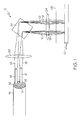
- the mirror array of the present invention can be used with or as part of an optical cross connect engine, such as a photonic or optical cross connection engine (“POXCE"), generally designated 12.
- POXCE photonic or optical cross connection engine
- a plurality of fiber optic cables 14 may be coupled to the optical cross connect engine 12.
- Each fiber optic cable 14 may include a plurality of individual optical fibers 16 encased therein.
- Each optical fiber 16 may carry or transport a light signal or beam 18.
- each beam 18 from each optical fiber 16 that is coupled to the optical cross connect engine 12 may be passed through a lens 20 that focuses each beam 18 upon a diffraction grating lens system 22.
- the grating lens system 22 can separate each beam 18 into a plurality of wavelength channel beams 19.
- Each wavelength channel beam 19 can represent a discreet wavelength that carries a signal, and each beam 18 and fiber 16 can typically carry a large number of discrete wavelength channel beams or signals, for example, up to 160 or more signals.
- the dispersed wavelength channel beams 19 may then be passed through a lens 24 and a quarter-wave plate 26 to compensate for the polarization sensitivity of the grating.
- the POXCE may utilize various methods and means for routing signals and beams, and need not necessarily include wavelength switching or other methods/components described above.
- the wavelength channel beams 19 may then reach the mirror array 10, also known as a micromechanical switching matrix.
- the mirror array 10 may include a plurality of movable mirrors or reflective surfaces such that the incoming signals 19 bounce off of the mirrors and are routed in the desired direction.
- the reflected signals 19 can then be passed back through the quarter-wave plate 26, lens 24, diffraction grating lens system 22 and lens 20, and may then be routed to the desired optical fiber 16 for further transportation.
- the mirror array 10 can redirect light signals from a departure optic fiber to a destination optic fiber.
- the departure optic fiber may be the same as the destination optic fiber ( Fig. 1 ), or they may be different (not shown in Fig. 1 ). Furthermore, the departure optic fiber may be in the same cable 14 as, or in a different cable from, the destination optic fiber. In other words, signals can be routed from any optic fiber connected to the cross connect engine to any optic fiber connected to the cross connect engine.
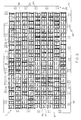
- the mirror array 10 may include a plurality of movable mirrors 30 formed in an array, with each mirror 30 including a reflective surface 31 located on an associated movable portion 32.
- the reflective surfaces 31 can be made from nearly any material that reflects the light signals to be transmitted (which can be infrared light).
- the reflective surfaces 31 can be made of a metal, such as gold. However, nearly any metal or material which can reflect the desired wavelength of energy may be used as the reflective material 31.
- the reflective material 31 may have a reflectivity of greater than about 95% at infrared wavelengths, and it has been found that gold is an appropriate material that may be used to reflect infrared radiation.
- Each of the mirrors 30 may be relatively small (i.e., in one embodiment on the order of about 20 microns x 20 microns), and the array 10 can include nearly any desired number of mirrors 30 (i.e., in one embodiment about 500 mirrors).
- Each movable portion 32 may be able to be rotated to move its associated reflective surface 31 into the desired configuration to reflect light signals in the desired manner.
- the mirrors 30 may be located on an upper wafer 34.
- the upper wafer 34 may include or be made up of two separate wafers or wafer portions which are joined together to form the upper wafer 34.
- the upper wafer 34 may thus be a silicon-on-insulator wafer, and/or be made of or include silicon-on-insulator wafers.
- the upper wafer 34 may include a base portion 36, and each of the movable portions 32 may be movably coupled to the base portion 36.
- each movable portion 32 may be defined by a set of cut outs or recesses 40, 42, 48, 50 formed in, and extending through the thickness of, the upper wafer 34.
- the inner cut outs 40, 42 may extend generally around the outer periphery of each movable portion 32.
- the ends of the inner cut outs 40, 42 may be slightly spaced apart to define a pair of narrow inner arms 44, 46 located on opposite sides of the associated movable portion 32.
- the portion of the upper wafer 34 located inside the inner cut outs 40, 42 may be rotatable about an axis A defined by the inner arms 44, 46.
- the upper wafer 34 may also include a set of outer cut outs 48, 50 that extend generally around the outer periphery of each movable portion 32.
- the ends of the outer cut outs 48, 50 may be spaced apart to define a pair of outer arms 52, 54 located on opposite sides of the associated movable portion 32.
- Each movable portion 28 may thus include an intermediate surface 58 located between the inner 40, 42 and outer 48, 50 cut outs. In this manner, the portions of the upper wafer 34 located inside of the outer cut outs 48, 50 (including the intermediate surface 58) may be rotatable about an axis B defined by the outer arms 52, 54.
- inner 40, 42 and outer 48, 50 cut outs and inner 44, 46 and outer 52, 54 arms define movable portions 32 that may double gimbaled, or independently pivotal, about both axes A and B.
- movable portions 32 may double gimbaled, or independently pivotal, about both axes A and B.
- various other structures and assemblies for pivotally and/or movable mounting mirrors 30, as well as various other biasing and spring mechanisms may also be used.
- the upper wafer 34 may be a silicon-on-insulator wafer which may include a lower silicon layer or support layer 60, an upper silicon layer 62, and an insulating layer 64 (such as silicon dioxide) located between the upper 60 and lower 62 silicon layers.
- the lower layer 60 may have a thickness of about 100 microns
- the upper layer 62 may have a thickness of about 10 microns (the relative thicknesses of the various layers are not necessarily shown in scale in the accompanying drawings).
- the insulating layer 64 (as well as the other insulating/passivation layers discussed herein) may be a silicon dioxide layer having a thickness of about 1 micron, but could also be nearly any insulating or dielectric layer of any desired thickness.
- the thickness and materials of the layers 60, 62, 64 can be varied as desired to meet the requirements of the array 10 or other microstructure.
- the lower layer 60 and upper layer 62, and in particular the upper layer 62, may be made of doped silicon or other semiconductor material such that the upper layer 62 has a relatively high electrical conductivity.
- the lower layer 60 and upper layer 62 can also be made from a variety of other materials besides silicon, such as amorphous silicon, polysilicon, silicon carbide, germanium, polyimide, ceramics, nitride, sapphire, silicon nitride, glasses, semiconductor material, a combination of these materials or nearly any other machinable or micromachinable material.
- the upper layer 62 may be electrically conductive or have an electrically conductive material located thereon such that the movable portion 32 can be moved by electrical or electrostatic forces, as will be discussed in greater detail below.
- the upper layer 62 may have the desired thickness of the movable portions 32 and associated arms 44, 46, 52, 54. More particularly, the cut outs 40, 42, 48, 50 may be formed in or through the upper layer 62 to form the intermediate portion 58 and inner arms 44, 46 and outer arms 52, 54.
- the upper wafer 34 may be coupled to a lower wafer 66 that is located below the upper wafer 34.
- the lower wafer 66 may be a silicon-on-insulator wafer having a silicon layer 67 and an insulating layer 69.
- the lower wafer 66 may include or be made up of two separate wafers or wafer portions which are joined together to form the lower wafer 66.
- the lower wafer 66 can also be a standard silicon wafer, or can be made of a variety of semiconducting materials beyond silicon, such as GaAs or InP, as well as the materials listed above for the upper wafer 34, or can also be or include a glass or ceramic substrate, or a printed circuit board.
- the upper wafer 34 and lower wafer 66 can be coupled together by a variety of methods and structures, including but not limited to benzocyclobutene (BCB) bonding (which will be discussed in greater detail below).
- the bond between the upper 34 and lower 66 wafers may be desired to be electrically insulating.
- relatively low temperature bonding or other coupling procedures for coupling the upper 34 and lower 66 wafers.
- adhesive or coupling medium having a reflow temperature of less than about 125° C, or to use a coupling procedure which takes place at a temperature less than about 125° C.
- the mirror array 10 may include a plurality of posts 68 that extend between the lower wafer 66 and upper wafer 34 and that may consist of bonding materials.
- posts 68 may extend between the upper 34 and lower 66 wafers in order to couple the wafers together, including portions of the upper 34 or lower 66 wafers themselves.
- the lower wafer 66 may include a plurality of electrodes or conductive surfaces 70, 72, 74, 76 located on an upper surface 75 of the lower wafer 66.
- the electrodes 70, 72, 74, 76 can be activated (such as by applying a voltage to the electrodes or a voltage across the electrodes and the mirrors 30, reflective surfaces 31 and/or movable portions 32) to control movement of the movable portions 32 and associated reflective surfaces 31.
- each mirror 30 may have an associated set of electrodes 70, 72, 74, 76 located below each mirror 30.
- the set of electrodes can include a pair of actuating electrodes 70, 72 and a pair of adjustment electrodes 74, 76.
- the lower wafer 66 may include a protective coating (not shown) such as an oxide or other passivation layer located on the lower surface 75, and in particular over the electrodes 70, 72, 74, 76 to protect the electrodes 70, 72, 74, 76 and prevent/limit oxidation thereof.
- a protective coating such as an oxide or other passivation layer located on the lower surface 75, and in particular over the electrodes 70, 72, 74, 76 to protect the electrodes 70, 72, 74, 76 and prevent/limit oxidation thereof.
- the mirror array 10 may include a plurality of solderable surfaces 88, or electrical connection sites 88, or flip chip connection sites 88, located around the perimeter of the array of mirrors 30.
- the flip chip connection sites 88 may be located on the lower wafer 66, and each of the flip chip connection sites 88 may include a plurality of pads 80 of conductive material.
- the pads 80 may be made of any desired material and formed by any of a wide variety of manufacturing methods.
- the pads 80 can be a eutectic alloy or other metal (such as solder, gold, or other metals), or other conductive materials, and can be formed, created or manufactured by evaporation, electroplating, screen printing, needle depositing, electroless plating, adhesive, or direct deposition.
- Each pad 80 may be made of a material or materials which are solderable surfaces; that is, surfaces which can be electrically or operatively coupled to another component or surface by solder connections.
- each pad 80 may include gold as the top-most layer, with the gold being located on a nickel layer, and the nickel layer being located on a titanium layer.
- the titanium layer may be located on an aluminum pad or other layer.
- each pad 80 can be made from a wide variety of materials to form solderable surfaces.
- the pads 80 may be formed to accommodate solder bump flip chips, plated bump flip chips, stud bump flip chips, adhesive bump flip chips, or other types of flip chips. Due to the materials of the pads 80 and flip chip bonding sites 88, the pads 80 and flip chip bonding sites 88 may be made of materials having a relatively low melting temperature, such as, for example, less than about 250°C, or less than about 300°C, or less than about 400°C. Thus, in subsequent processing steps care should be taken to not exceed the melting point of the pads 80 and flip chip bonding sites 88.
- twenty-five pads 80 are arranged in a 5x5 array to form a connection site 88.
- at least one of the pads 80, or each of the pads 80 may be electrically or operatively coupled to at least one of the electrodes 70, 72, 74, 76 to control the actuation of the electrodes 70, 72, 74, 76, and each pad 80 may be electrically isolated from any adjacent pads 80.
- connection sites 88 may be arranged to be electrically or operatively coupled to a chip 81 or other electronic component that is located on and supported by the lower wafer 66.
- each connection site 88 may be able to accept a chip 81 thereon by flip chip bonding or flip chip coupling (also known as direct chip attach) which involves placing a chip, having electrical contacts, directly onto the flip chip connection sites 80 so that the contacts of the chip are electrically and/or operatively coupled to the pads 80 in a well known manner.
- a chip 81 having a plurality of output bumps or contacts 83 is located on top of and coupled to the connection site 88, pads 80 and/or lower wafer 66.
- connection site 88 such as by soldering, conductive adhesive, etc.
- the pads 80 may thus be arranged in the same pattern of the output contacts 83 to ensure that the connection sites 88 are shaped to properly receive a chip 81 thereon.
- the connection sites 88 as including a square 5x5 array of pads 80
- the pads 80 may be sized, shaped and arranged in nearly any manner to accommodate the size, shape and arrangement of output contacts 83 of the flip chip 81 desired to be used with the array 10.
- the chip 81 may be any electronic component, including a processor, electronics, memory, circuitry, ASIC, processor, controller, logic chip, or the like, and may include a plurality of transistors, such as CMOS transistors (not shown).
- the chip 81 may provide the logic circuitry for controlling the application of voltages to the electrodes 70, 72, 74, 76.
- the chip 81 may include nearly any electronic component(s) that can provide the logic and routing circuitry for directing the desired voltages to the electrodes 70, 72, 74, 76 in the desired manner.
- CMOS transistors may be preferred as the logic circuitry and as a high voltage driver because CMOS transistors use relatively low amounts of power and generate relatively little heat.
- the CMOS transistors or other logic circuitry may be coupled together in a multiplexed fashion.
- the chip 81 may include an external connection location 85 to enable the chip 81 to be connected to an external processor, printed circuit board, controller, computer, CPU or the like, for example, via a wire bond, ribbon, or other connection method.
- the chip 81 may be coupled to a PCB with wirebonds, and the PCB may be coupled to a processor, controller or computer with a ribbon cable.
- Fig. 8 illustrates only a single chip 81, additional ones of the connection sites 88, or all of the connection sites 88 of the array 10, may include a chip 81 located thereon, and each of the chips 81 may be coupled to external processor, controller, computer, CPU or the like.
- Each chip 81 may be electrically connected or coupled to electrodes 70, 72, 74, 76 for selected ones of the mirrors 30, or be electrically connected or coupled to electrodes 70, 72, 74, 76 for selected rows and/or columns of the mirrors 30.
- Each chip 81 may also be electrically connected or coupled to the mirrors 30 (i.e. to the reflective surfaces 31) so that a voltage differential between the electrodes 70, 72, 74, 76 and the mirrors 30 can be maintained and controlled.
- the mirrors 30 i.e. the reflective surfaces 31
- the mirrors 30 may instead be grounded so that the voltage differential between the electrodes 70, 72, 74, 76 can be precisely known.
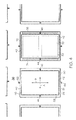
- the upper wafer 34 in top view is generally rectangular and is located within the perimeter of the generally rectangular lower wafer 66.
- the upper wafer 34 is located within or contained within the "coverage area" or “footprint” of the lower wafer 66 in top view.
- the lower wafer 66 includes an "underhang” portion 87 protruding outwardly relative to the upper wafer 34, or not covered by or located under the upper wafer 34.
- connection sites 88 may be located on the underhang portion 87 to ensure that the connection sites 88 can be easily accessed to enable a chip 81 to be easily coupled to each connection site 88.
- each connection site 88, as well as each chip 81 may be located outside the coverage area or footprint of the upper wafer 34.
- the footprint of the lower wafer 66 need not necessarily be larger than the footprint of the upper wafer 34. Instead, all that is required is that the lower wafer 66 have a surface upon which a connection site 88 can be located, wherein that surface is not covered by or located below the upper wafer 34.
- the underhang portion 87 provides a surface upon which a chip 81 can be easily coupled.
- the coverage area or footprint of the upper wafer 34 may be viewed as the shadow cast by the upper wafer 34 by a light source located directly above the upper wafer 34.
- the portions of the lower wafer 66 which are not located directly below a portion of the upper wafer 34 may be considered to be outside the coverage area of the upper wafer, even if those portions of the lower wafer 66 are located away from the outer perimeter of the upper wafer 66 (i.e. are located below an opening formed in the upper wafer 34) or adjacent to irregular outer edges of the upper wafer 34.
- connection sites 88 which can receives chips 81 thereon, the entire array 10 can be manufactured without having any chips or complex electronics located on the array 10, which can be suspect to damage during manufacturing.
- the chips 81 may then be coupled to the connection sites 88 as a final assembly step.
- the manufacturing of the mirrors 30 and the body of the array 10 can be manufactured separately from the electronics or chips 81.
- unacceptable arrays 10 and chips 81 can be discarded before assembly, thereby improving the yield of the end product.
- the use of a chip 81 and flip chip manufacturing also reduces the need for wire bonding and improves efficiency of manufacturing and the robustness of the array 10, and may reduce parasitic effects and improve transmission speed.
- a processor, controller, computer or CPU or the like is connected to all or selected ones of the chips 81.
- the controller can then provide signals to the chips 81, which are processed and analyzed by the chips 81 to determine how to apply various voltages in the desired manner to the desired electrodes 70, 72, 74, 76. Further, a specific mirror or mirrors, or mirror address(es) may be provided from the controller for actuation.
- a positive or negative AC or DC voltage may be applied to the actuating electrode 72 (i.e. across the electrode 72 and the associated mirror 30).
- the amount of voltage applied to the electrode 72 can be any amount of voltage to achieve the desired rotation, for example, in one case about 200 volts.
- the mirror 30 and/or reflective surface 31 and/or movable portion 32 may be grounded by, for example, grounding each mirror to the bulk of the upper wafer 34.
- the voltages in the actuating electrode 72 creates an electrostatic force that causes the conductive movable portion 32 to rotate in the direction of arrow C (i.e., about axis A and about inner arms 44, 46 (see Figs.
- each mirror 30 can be rotated to the desired inclination to reflect an incoming light signal in the desired direction.
- the inner arms 44, 46 are twisted or placed in a state of tension/compression.
- the movable portion 32 and mirror 30 may rotate in the direction opposite to arrow C to return the movable portion 32 to its neutral position shown in Fig. 6 .
- the spring force of the inner arms 44, 46 returns the movable portion 32 and mirror 30 to their neutral position.
- the movable portion 32 can be moved in the direction opposite to arrow C by applying a voltage to electrode 70 while the mirror 30 is grounded.
- the adjustment electrodes 74, 76 can be used to provide another degree of freedom to the movable portion 32.
- a voltage can be applied to the adjustment electrodes 74, 76 to set up an electrical field that can cause the movable portion to rotate about the outer arms 52, 54 (about axis B of Fig. 4 ) and in the directions of arrow D ( Fig. 7 ).
- the external controller and/or the chips 81 can execute control over each set of electrodes 70, 72, 74, 76 associated with each movable portion 32 and mirror 30 to simultaneously control the movement of each mirror 30.
- the array 10 can thereby be controlled by the controller and/or chips 81 to reflect a large number of beams of light signals to carry out the switching function of the mirror array 10.
- the mirrors 30 may be grounded so that the voltage differential between the electrodes 70, 72 and the mirrors 30 can be precisely controlled.
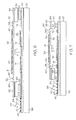
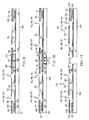
- Figs. 9-11 illustrate a method for forming/singulating the mirror array 10 of Figs. 2-8 , although various other methods of forming the mirror array 10 may be used without departing from the scope of the invention.
- the array 10 may be batch processed such that a plurality of movable portions, reflective surfaces, mirrors, electrodes, control electronics and the like are simultaneously formed on a wafer or wafers.
- Figs. 9-11 illustrate only two adjacent mirrors and the associated components being formed.
- Figs. 9-11 are representative cross-sections which are intended to illustrate various features of the manufacturing process, and may not identically represent a cross-section of the device.
- Fig. 11 illustrates two adjacent mirrors 30. However, it should be understood that each mirror 30 shown in Fig. 11 may be only a single mirror in an array of mirrors.
- the left-hand mirror 30 shown in Figs. 11 may be only a single mirror 30 of a larger array 10a and the right-hand mirror 30 may be only a single mirror in a larger array 10b.
- the process may begin by providing/forming an upper wafer 34 which can include a plurality of inner arms 44, 46, outer arms 52, 54, base portions 36, movable portions 32, cut outs 40, 42, 48, 50, etc.
- the inner arms 44, 46, outer arms 52, 54, base portions 36, movable portions 32, cut outs 40, 42, 48, 50 can be formed by various processes and methods, including deep reactive ion etching ("DRIE") through upper wafer 34 or the upper layer 62 of the upper wafer 34.
- DRIE deep reactive ion etching
- the movable portions 32 may or may not include the reflective material 30 located thereon.
- the upper wafer 34 may be processed to various stages of completion, and in the illustrated embodiment the upper wafer 34 is nearly completely processed except for the addition of the reflective material 30.
- a lower wafer 66 may then be provided.
- the lower wafer 66 may also include the metallization portions located thereon, such as a plurality of electrodes 70, 72, 74, 76, pads 80 and bonding sites 88.
- the pads 80 and bonding sites 88 may be formed on what will ultimately form the underhang portions 87.
- the upper wafer 34 may then be bonded or coupled to the lower wafer 66. Any of a wide variety of methods for attaching the upper 34 and lower 66 wafers may be used. However, it may be preferred that the upper 34 and lower 66 wafers be coupled at a relatively low temperature, such as, for example, temperatures less than about 250°C to protect the solderable surfaces, such as the bonding sites 88 and pads 80. Low temperature bonding can also reduce the stress effects caused by materials having differing coefficients of thermal expansion, reduce the diffusive migration and oxidation of materials, and provide a process which is easier to control and implement.
- a relatively low temperature such as, for example, temperatures less than about 250°C to protect the solderable surfaces, such as the bonding sites 88 and pads 80.
- Low temperature bonding can also reduce the stress effects caused by materials having differing coefficients of thermal expansion, reduce the diffusive migration and oxidation of materials, and provide a process which is easier to control and implement.
- the bonding or coupling process may take place at a temperature below the melting or reflow temperature of the metallization of the lower wafer 66, such as the pads 80 and flip chip connection sites 88.
- a bonding or coupling process which can take place at temperatures below 400°C, or below 300°C, or below 250°C may be used to couple the upper wafer 34 and lower wafer 66.
- the upper 34 and lower 66 wafer are coupled by a BCB bonding process, which is discussed in detail below and shown in Figs. 12-14 .
- the BCB or other suitable bonding processes may protect the metallization of the lower wafer 66, which may have a melting or reflow temperature of around or below 250°C, 300°C or 400°C.
- the upper 34 and lower 66 wafers may be processed to various stages of completion prior to their bonding or coupling, and further processing of the upper 34 and lower 66 wafers after bonding or coupling may be required to produce the upper 34 and lower 66 wafers in their states shown in Fig. 9 .
- a pair of upper singulation etches or cavities 91 may be formed through the thickness of the upper wafer 34, and the lower wafer 66 may then be etched to include a pair of lower singulation cavities 89, or partial etches, formed through a portion of the thickness of the silicon layer 67. Either or both of he upper singulation cavities 91 and lower singulation cavities 89 may also be formed prior to coupling the upper wafer 34 and lower wafer 66 together.
- the cavities 89, 91 may be formed by DRIE or other suitable etching methods.
- the lower singulation cavities 89 do not extend entire through the thickness of the lower wafer 66, but may extend more than one half the thickness of the silicon layer 67, such as, for example, about 2/3 through the thickness of the silicon layer 67 to leave a relative thin tab 95 above the singulation cavities 89.
- both or either of the singulation cavities 89, 91 may extend completely or partially through the associated wafer.
- the singulation cavities 89, 91 may be formed in or adjacent to a body portion 93 located between two separate arrays 10a, 10b which are desired to be singulated (i.e. separated or divided).
- a plurality of singulation cavities 89, 91 beyond those shown in Fig. 10 may be formed or etched wherever the wafers 34, 66 are desired to be singulated or separated into sub-wafers or wafer portions
- Each of the cavities 89, 91 may extend generally vertically, or generally perpendicular to the arrays 10a, 10b, or generally perpendicular to the wafers 34, 66.
- the upper singulation cavities 91 may be laterally offset from (i.e. not vertically aligned with) the lower singulation cavities 89.
- each upper singulation cavity 91 may be located closer to the associated, adjacent mirror 30 or array 10a, 10b than the associated lower singulation cavity 89.
- the left hand upper singulation cavity 91 may be located closer to the left hand mirror 30 or movable portion 32 of Fig.
- the right hand upper singulation cavity 91 may be located closer to the right hand mirror 30 or movable portion 32 than the right hand lower singulation cavity 89.
- the offset nature of the singulation cavities 89, 91 enable the adjacent arrays 10a, 10b to have the underhang portion 87 upon which the bonding sites 88 and chip 81 can be located.
- the reflective material 31, such as gold or another metal may then be deposited on the movable portions 32 to form the mirrors 30 thereon.
- the reflective material may be deposited by sputtering a metal through a shadow mask and onto the movable portion 32, or by any other acceptable process.
- each of the arrays 10a, 10b is singulated along a dividing line 97 ( Fig. 10 ) which includes two offset, generally vertically extending portions (defined at least partially by the cavities 89, 91)
- the tab 95 can be located at nearly any location throughout the thickness of the of the upper 34 or lower 66 wafers and need not necessarily be located above the lower singulation cavity 89. Further, instead of having two spaced lower cavities 89, only a single lower cavity 89 may be used.
- a cap (not shown) may be coupled to and located over each array 10a, 10b to protect the mirrors 30.
- a chip or chips 81 can then be coupled to the bonding sites 88.
- Each chip 81 may then be coupled to the associated bonding site 88, such as by flip chip bonding or other coupling processes, and the chip 81 and/or bonding sites 88 may be under filled in a well-known manner.
- Each array 10a, 10b can then be located in or formed as part of an optical cross-connect engine.
- Figs. 9-11 illustrate a process for coupling upper 34 and lower 66 wafers together to form a micro mirror array
- the singulation process described herein which may be implement using offset cavities or etching, can be utilized to singulate nearly any desired micromachine, micro device, microelectromechanical structure, and the like.
- the lower wafer 66 and upper wafer 34 may each be at least partially premanufactured and tested before they are joined together. Further, the chips 81 can be manufactured or acquired separately.
- This modular manufacturing provides greater flexibility in manufacturing the mirror array 10 and raises the overall yield of the arrays 10. For example, a number of upper 34 and lower 66 wafers can be premanufactured and tested according to varying specifications, and the premanufactured and approved upper 34 and lower 66 wafers can then be stored. A number of chips 81 having varying specifications can also be manufactured or acquired and tested.
- the upper 34 and lower 66 wafers and chips 81 that correspond to the parameters of the desired array can then be obtained, joined together and processed to completion. Furthermore, premanufacturing the wafers 34, 66 and chips 81 enables any faulty wafers 34, 66 or chips 81 to be detected and disposed of before they are coupled together which thereby increases the overall yield of the array manufacturing process.
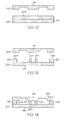
- Figs. 12-14 illustrate one method for coupling the upper 34 and lower 66 wafers together, such as during the step shown in Fig. 9 above.
- Fig. 12-14 illustrate two generic wafers 200, 202 being coupled together, although it should be understood that the wafers 200, 202 can correspond to the upper 34 and lower 66 (as well as any other wafers which are desired to be coupled).
- the wafers 200, 202 may first be cleaned and an adhesion promoter may be applied to the wafers 200, 202.
- a layer of benzocyclobutene (“BCB” trade name CYCLOTENE® 4024-40 manufactured by the Dow Chemical Company of Midland, Michigan), which is a negative tone photoresist, 204 may be applied to at least one of the wafers 200, 202, such as by spinning the BCB layer 204 thereon. ( Fig. 12 ). Materials other than BCB may also be used as the bonding layer 204.
- polyimide, SU8 (a negative, epoxy-type, near-UV photoresist based on EPON SU-8 epoxy resin sold by Shell Chemical), or other patternable or photopatternable adhesives with a low cure temperature may be used.
- the layer 204 may be spun to any desired thickness, such as a thickness of between about 0.25 microns or less and about 20 microns or more, and in one embodiment the layer 204 has a thickness of about 4.5 microns.
- the layer 204 may be exposed to a "soft bake" to at least partially harden the layer 204 for subsequent photopatterning.
- the soft bake includes exposing the wafer 200 to a temperature of about of about 75°C for about 180 seconds. However, the soft bake may be carried out for sufficient time and under sufficient temperatures until the layer 204 is sufficiently hardened or cured to allow photopatterning of the layer 204, while still allowing sufficient solvents to remain in the layer 204 for subsequent bonding. The soft bake elevates the glass transition temperature of the BCB for safe handling at room temperature.
- the layer 204 may be patterned by, for example, exposing portions of the layer 204 which are desired to remain to electromagnetic (i.e. UV) radiation while shielding portions of the layer 204 which are not desired to be removed from the radiation.
- the UV radiation initiates crosslinking in the exposed portions of the layer 204 while the shielded portions of the layer 204 are protected, such as by a mask, from the radiation to prevent crosslinking.
- any portions of the wafer 200 (or wafers 34, 66) which are desired to be contacted and adhered to the wafer 202 may be exposed to the radiation.
- the layer 204 may then undergo a pre-develop bake to further encourage crosslinking of portions of the layer 204 which are not desired to be removed.
- the pre-develop bake may include exposure to a temperature of about 75°C for about 90 seconds. However, the pre-develop bake may be carried out for sufficient times and under sufficient temperatures until the portions of the layer 204 which are desired to remain are sufficiently crosslinked.
- the non-crosslinked portions of the layer 204 may then be removed in a develop process using a puddle or immersion developer process.
- the wafer 200 may then be dried thereby resulting in the wafers 200, 202 shown in Fig. 13 .
- the wafer 200 may then be cleaned in a "descumming" process to remove any residual, dilute BCB on the wafer 200.
- the layer 204 may then be allowed to cure at room temperature (i.e. about 68°F or 20°C) for about 8 hours. However, this BCB cure step may be carried out for sufficient times and under sufficient temperatures to raise the glass transition temperature of the layer 204 to provide a stable BCB layer 204 and control reflow of the layer 204 during subsequent processing (except for during bonding). This BCB cure step further elevates the glass transition temperature of the layer 204 in preparation of bonding.
- the wafers 200, 202 may then be placed into contact in the desired orientation and pressed together for bonding ( Fig. 14 ).
- the bond is cured by exposing the wafers 200, 202 to temperature of about 250°C under a force of about 1001b for about 30 minutes.
- this bond cure step may be carried for sufficient times and under sufficient temperatures and pressures until the portions of the layer 204 form a sufficient bond between the wafers 200, 202.
- BCB layer 204 provides a photopatternable adhesive for the wafers 200, 202 so that the adhesive 204 can be easily patterned and arranged in the desired manner. Further, the layer 204 can be easily deposited, provides wafer rework capabilities and is generally homogeneous.
- BCB or other similar materials can also be used as a passivation or electrical isolation layer.
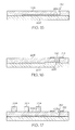
- a BCB passivation layer 206 can be located over any conductive portions or layers which are desired to be isolated, such as a metallic interconnect layer 208.
- the passivation layer 206 can be located on the wafer 200/interconnect layer 208 and spun to form an even coating having nearly any desired thickness.
- the soft bake and photo patterning steps described above in the context of Figs. 12-14 may then be used so that undesired portions of the passivation layer 206 are removed.
- the passivation layer 206 may be etched to form a via 210 to expose at least a portion of the metal interconnect 208.
- the passivation layer 206 may then be "hard” cured to generally fully cure the BCB and generally drive out any solvents to provide a hard, stable passivation layer 206.
- the hard cure may raise the glass transition temperature of the passivation layer 206 beyond bond temperatures so that any subsequent bonding steps involving the wafer 200 do not affect or cause reflow of the passivation layer 206, and so that the passivation layer 206 is generally insensitive to light and generally inert to BCB ancillary chemical and etchants.
- leads 212 may then be deposited onto the passivation layer 206 and in contact with the metal interconnect 208.
- a bonding layer 204 (such as BCB) may be located on top of the passivation layer 206.
- the bonding layer 204 may then be etched, baked, cured, and otherwise processed as described above in order to enable the wafer 202 to be coupled to the wafer 200.
- Fig. 17 illustrates the bonding layer 204 after etching.
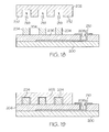
- Wafer 202 which is desired to be coupled to wafer 200, may then be provided, as shown in Fig. 18 .
- wafer 202 includes a plurality of cutouts or notches 219 formed therein, with each notch being sized and located to receive a portion of the BCB bonding layer 204 therein.
- the wafer 202 may then be located on top of passivation layer 206 and the bonding layer 204, as shown in Figs. 18 and 19 .
- Heat and temperature are then applied to the wafer stack to bond the wafer 202 to the wafer 200 as described above in the context of Fig. 14 .
- the wafer 200 may be bonded to the wafer 202 at a temperature above the glass transition temperature of the bonding layer 204, but below the glass transition temperature of the passivation layer 206.
- the passivation layer 206 may be located between any portions of the wafers 200, 202 to ensure that the wafers 200, 202 remain electrically isolated due to the dielectric qualities of BCB.
- the lower or bond surface 232 of the wafer 202 contacts the passivation layer 206, instead of the lead 208.
- the passivation layer 206 electrically isolates the wafer 202 from the lead 208, and from the wafer 200.
- the layer 206 can be used as a passivation layer.
- the bonding and bonding/passivation step shown in Figs. 15-19 may be used for nearly any wafer or wafer portions.
- the bonding and bonding/passivation method as disclosed therein may be used in any microstructure to couple and/or passivate a microstructure or various portions of a microstructure.
- Such microstructures may, in one embodiment, include the array 10 disclosed herein, but the processes disclosed herein can also be used with a wide variety of other microstructures beyond the array 10, including a wide variety of sensors or actuators.
Landscapes
- Engineering & Computer Science (AREA)
- Microelectronics & Electronic Packaging (AREA)
- Manufacturing & Machinery (AREA)
- Physics & Mathematics (AREA)
- General Physics & Mathematics (AREA)
- Optics & Photonics (AREA)
- Micromachines (AREA)
- Mechanical Light Control Or Optical Switches (AREA)
Applications Claiming Priority (2)
| Application Number | Priority Date | Filing Date | Title |
|---|---|---|---|
| US10/620,119 US7203394B2 (en) | 2003-07-15 | 2003-07-15 | Micro mirror arrays and microstructures with solderable connection sites |
| EP04103379A EP1498764A3 (de) | 2003-07-15 | 2004-07-15 | Anordnung von Mikrospiegeln und Mikrostrukturen mit lötbaren Verbindungsstellen |
Related Parent Applications (1)
| Application Number | Title | Priority Date | Filing Date |
|---|---|---|---|
| EP04103379A Division EP1498764A3 (de) | 2003-07-15 | 2004-07-15 | Anordnung von Mikrospiegeln und Mikrostrukturen mit lötbaren Verbindungsstellen |
Publications (1)
| Publication Number | Publication Date |
|---|---|
| EP1953583A2 true EP1953583A2 (de) | 2008-08-06 |
Family
ID=33477089
Family Applications (2)
| Application Number | Title | Priority Date | Filing Date |
|---|---|---|---|
| EP08153865A Withdrawn EP1953583A2 (de) | 2003-07-15 | 2004-07-15 | Mikrospiegelarrays und Mikrostrukturen mit lötbaren Verbindungsstellen |
| EP04103379A Withdrawn EP1498764A3 (de) | 2003-07-15 | 2004-07-15 | Anordnung von Mikrospiegeln und Mikrostrukturen mit lötbaren Verbindungsstellen |
Family Applications After (1)
| Application Number | Title | Priority Date | Filing Date |
|---|---|---|---|
| EP04103379A Withdrawn EP1498764A3 (de) | 2003-07-15 | 2004-07-15 | Anordnung von Mikrospiegeln und Mikrostrukturen mit lötbaren Verbindungsstellen |
Country Status (3)
| Country | Link |
|---|---|
| US (1) | US7203394B2 (de) |
| EP (2) | EP1953583A2 (de) |
| JP (1) | JP2005062881A (de) |
Cited By (6)
| Publication number | Priority date | Publication date | Assignee | Title |
|---|---|---|---|---|
| CN106415361B (zh) * | 2014-01-19 | 2018-11-13 | 苹果公司 | 用于装有万向接头的扫描镜阵列的耦接方案 |
| US10168530B2 (en) | 2012-03-22 | 2019-01-01 | Apple Inc. | Coupling schemes for gimbaled scanning mirror arrays |
| US10247812B2 (en) | 2012-03-22 | 2019-04-02 | Apple Inc. | Multi-mirror scanning depth engine |
| US10330921B2 (en) | 2015-02-16 | 2019-06-25 | Apple Inc. | Hybrid MEMS scanning module |
| US10488652B2 (en) | 2016-09-21 | 2019-11-26 | Apple Inc. | Prism-based scanner |
| US11604347B2 (en) | 2019-08-18 | 2023-03-14 | Apple Inc. | Force-balanced micromirror with electromagnetic actuation |
Families Citing this family (17)
| Publication number | Priority date | Publication date | Assignee | Title |
|---|---|---|---|---|
| US20060211233A1 (en) * | 2005-03-21 | 2006-09-21 | Skyworks Solutions, Inc. | Method for fabricating a wafer level package having through wafer vias for external package connectivity and related structure |
| US7287687B2 (en) * | 2005-03-22 | 2007-10-30 | I.C.A.R.D., L.L.C. | System and method for regulating alcohol consumption |
| US7576426B2 (en) * | 2005-04-01 | 2009-08-18 | Skyworks Solutions, Inc. | Wafer level package including a device wafer integrated with a passive component |
| JP4935013B2 (ja) * | 2005-07-21 | 2012-05-23 | ブラザー工業株式会社 | 光走査装置、画像表示装置及び光スキャナの共振周波数変更方法並びに反射ミラー位置の補正方法 |
| JP2007108753A (ja) * | 2005-10-11 | 2007-04-26 | Samsung Electro Mech Co Ltd | メムスパッケージおよび光変調器モジュールパッケージ |
| US20100172483A1 (en) * | 2006-02-21 | 2010-07-08 | Vimplicity Ltd. | Conversation of a phone call into a smart pushed voice message |
| US7449765B2 (en) * | 2006-02-27 | 2008-11-11 | Texas Instruments Incorporated | Semiconductor device and method of fabrication |
| US7635606B2 (en) * | 2006-08-02 | 2009-12-22 | Skyworks Solutions, Inc. | Wafer level package with cavities for active devices |
| US20080217708A1 (en) * | 2007-03-09 | 2008-09-11 | Skyworks Solutions, Inc. | Integrated passive cap in a system-in-package |
| US20080309936A1 (en) * | 2007-06-18 | 2008-12-18 | Oxford Instruments Analytical Oy | Spectrometer with multiple gratings |
| US8324728B2 (en) * | 2007-11-30 | 2012-12-04 | Skyworks Solutions, Inc. | Wafer level packaging using flip chip mounting |
| US8900931B2 (en) | 2007-12-26 | 2014-12-02 | Skyworks Solutions, Inc. | In-situ cavity integrated circuit package |
| DE102008004639A1 (de) | 2008-01-16 | 2009-07-23 | Robert Bosch Gmbh | Mikromechanisches Bauteil und Herstellungsverfahren für ein mikromechanisches Bauteil |
| CH699109A1 (fr) * | 2008-07-10 | 2010-01-15 | Swatch Group Res & Dev Ltd | Procédé de fabrication d'une pièce micromécanique. |
| TWI388038B (zh) * | 2009-07-23 | 2013-03-01 | 財團法人工業技術研究院 | 感測元件結構與製造方法 |
| US9335544B2 (en) * | 2013-03-15 | 2016-05-10 | Rit Wireless Ltd. | Electrostatically steerable actuator |
| US11274035B2 (en) * | 2019-04-24 | 2022-03-15 | X-Celeprint Limited | Overhanging device structures and related methods of manufacture |
Family Cites Families (23)
| Publication number | Priority date | Publication date | Assignee | Title |
|---|---|---|---|---|
| US5096279A (en) * | 1984-08-31 | 1992-03-17 | Texas Instruments Incorporated | Spatial light modulator and method |
| JPH06120336A (ja) | 1992-10-02 | 1994-04-28 | Matsushita Electric Works Ltd | センサー用微細加工素子ウェハの切断方法 |
| JPH08106614A (ja) | 1994-10-04 | 1996-04-23 | Iwatsu Electric Co Ltd | 微細加工による電気回路用ボンディングパッドの形成方法 |
| US5757536A (en) * | 1995-08-30 | 1998-05-26 | Sandia Corporation | Electrically-programmable diffraction grating |
| US5721162A (en) * | 1995-11-03 | 1998-02-24 | Delco Electronics Corporation | All-silicon monolithic motion sensor with integrated conditioning circuit |
| US5999306A (en) * | 1995-12-01 | 1999-12-07 | Seiko Epson Corporation | Method of manufacturing spatial light modulator and electronic device employing it |
| US5923995A (en) | 1997-04-18 | 1999-07-13 | National Semiconductor Corporation | Methods and apparatuses for singulation of microelectromechanical systems |
| DE19857946C1 (de) * | 1998-12-16 | 2000-01-20 | Bosch Gmbh Robert | Mikroschwingspiegel |
| US6426282B1 (en) * | 2000-05-04 | 2002-07-30 | Applied Materials, Inc. | Method of forming solder bumps on a semiconductor wafer |
| KR100332967B1 (ko) * | 2000-05-10 | 2002-04-19 | 윤종용 | 디지털 마이크로-미러 디바이스 패키지의 제조 방법 |
| US6525864B1 (en) * | 2000-07-20 | 2003-02-25 | Nayna Networks, Inc. | Integrated mirror array and circuit device |
| US20020110312A1 (en) * | 2000-07-20 | 2002-08-15 | Nayna Networks, Inc. | Integrated mirror array and circuit device with improved electrode configuration |
| US6291317B1 (en) * | 2000-12-06 | 2001-09-18 | Xerox Corporation | Method for dicing of micro devices |
| US6711317B2 (en) * | 2001-01-25 | 2004-03-23 | Lucent Technologies Inc. | Resiliently packaged MEMs device and method for making same |
| US6480320B2 (en) * | 2001-02-07 | 2002-11-12 | Transparent Optical, Inc. | Microelectromechanical mirror and mirror array |
| WO2002095800A2 (en) * | 2001-05-22 | 2002-11-28 | Reflectivity, Inc. | A method for making a micromechanical device by removing a sacrificial layer with multiple sequential etchants |
| AU2002305835A1 (en) * | 2001-06-08 | 2002-12-23 | The Regents Of The University Of Michigan | Low-temperature patterned wafer bonding with photosensitive benzocylobutene (bcb) and 3d microelectromechanical systems fabrication |
| US6587613B2 (en) * | 2001-07-24 | 2003-07-01 | Innovative Technology Licensing, Llc | Hybrid MEMS fabrication method and new optical MEMS device |
| ATE393409T1 (de) * | 2001-10-19 | 2008-05-15 | Ion Geophysical Corp | Digitale optische schaltvorrichtung und prozess zu ihrer herstellung |
| US20030122206A1 (en) * | 2001-11-09 | 2003-07-03 | Amal Bhattarai | Multi-chip module integrating MEMS mirror array with electronics |
| US6781239B1 (en) * | 2001-12-05 | 2004-08-24 | National Semiconductor Corporation | Integrated circuit and method of forming the integrated circuit having a die with high Q inductors and capacitors attached to a die with a circuit as a flip chip |
| US20030107794A1 (en) * | 2001-12-11 | 2003-06-12 | Siekkinen James W. | Micro mirror array |
| US7033672B2 (en) * | 2002-03-19 | 2006-04-25 | Analog Devices, Inc. | Static dissipation treatments for optical package windows |
-
2003
- 2003-07-15 US US10/620,119 patent/US7203394B2/en not_active Expired - Fee Related
-
2004
- 2004-07-15 EP EP08153865A patent/EP1953583A2/de not_active Withdrawn
- 2004-07-15 JP JP2004235666A patent/JP2005062881A/ja active Pending
- 2004-07-15 EP EP04103379A patent/EP1498764A3/de not_active Withdrawn
Cited By (6)
| Publication number | Priority date | Publication date | Assignee | Title |
|---|---|---|---|---|
| US10168530B2 (en) | 2012-03-22 | 2019-01-01 | Apple Inc. | Coupling schemes for gimbaled scanning mirror arrays |
| US10247812B2 (en) | 2012-03-22 | 2019-04-02 | Apple Inc. | Multi-mirror scanning depth engine |
| CN106415361B (zh) * | 2014-01-19 | 2018-11-13 | 苹果公司 | 用于装有万向接头的扫描镜阵列的耦接方案 |
| US10330921B2 (en) | 2015-02-16 | 2019-06-25 | Apple Inc. | Hybrid MEMS scanning module |
| US10488652B2 (en) | 2016-09-21 | 2019-11-26 | Apple Inc. | Prism-based scanner |
| US11604347B2 (en) | 2019-08-18 | 2023-03-14 | Apple Inc. | Force-balanced micromirror with electromagnetic actuation |
Also Published As
| Publication number | Publication date |
|---|---|
| US7203394B2 (en) | 2007-04-10 |
| US20050013533A1 (en) | 2005-01-20 |
| JP2005062881A (ja) | 2005-03-10 |
| EP1498764A2 (de) | 2005-01-19 |
| EP1498764A3 (de) | 2006-07-05 |
Similar Documents
| Publication | Publication Date | Title |
|---|---|---|
| US7203394B2 (en) | Micro mirror arrays and microstructures with solderable connection sites | |
| US6912078B2 (en) | Electrostatically actuated micro-electro-mechanical devices and method of manufacture | |
| US7192796B2 (en) | Methods and apparatus for packaging integrated circuit devices | |
| US6563106B1 (en) | Micro-electro-mechanical-system (MEMS) mirror device and methods for fabricating the same | |
| US6872319B2 (en) | Process for high yield fabrication of MEMS devices | |
| KR100676493B1 (ko) | 재배선 기판을 이용한 웨이퍼 레벨 칩 스케일 패키지의제조 방법 | |
| EP1400487B1 (de) | MEMS enthaltende Halbleitereinheit | |
| EP1351089B1 (de) | Optischer Schalter | |
| US6014240A (en) | Method and apparatus for an integrated laser beam scanner using a carrier substrate | |
| US7807506B2 (en) | Microelectromechanical semiconductor component with cavity structure and method for producing the same | |
| US20030102777A1 (en) | Ultrasonic transducer and method of manufacturing the same | |
| US6686639B1 (en) | High performance MEMS device fabricatable with high yield | |
| US20030122206A1 (en) | Multi-chip module integrating MEMS mirror array with electronics | |
| US8212344B2 (en) | Microelectromechanical semiconductor component with cavity structure and method for producing the same | |
| USRE38437E1 (en) | Method and apparatus for an integrated laser beam scanner using a carrier substrate | |
| US20030107794A1 (en) | Micro mirror array | |
| CA2463900A1 (en) | Digital optical switch apparatus and process for manufacturing same | |
| JP2005228863A (ja) | 半導体装置の製造方法、半導体装置及びセンサ | |
| US6743653B2 (en) | Micromachine manufacturing method | |
| JP3836809B2 (ja) | マイクロマシンの製造方法 | |
| JP3983176B2 (ja) | ミラー基板の製造方法及び光スイッチ装置の製造方法 | |
| WO2003073505A1 (en) | Integrated circuit device and method of manufacturing thereof | |
| KR102673474B1 (ko) | 마이크로 전자 기계 시스템 및 그 제조 방법 | |
| KR20030050799A (ko) | 정전구동 마이크로미러 및 그 제조방법, 그를 이용한광스위치 | |
| WO2025134091A1 (en) | Asic integrated mems device with exposed bond-pads from bottom attached asic and making the same |
Legal Events
| Date | Code | Title | Description |
|---|---|---|---|
| PUAI | Public reference made under article 153(3) epc to a published international application that has entered the european phase |
Free format text: ORIGINAL CODE: 0009012 |
|
| AC | Divisional application: reference to earlier application |
Ref document number: 1498764 Country of ref document: EP Kind code of ref document: P |
|
| AK | Designated contracting states |
Kind code of ref document: A2 Designated state(s): AT BE BG CH CY CZ DE DK EE ES FI FR GB GR HU IE IT LI LU MC NL PL PT RO SE SI SK TR |
|
| STAA | Information on the status of an ep patent application or granted ep patent |
Free format text: STATUS: THE APPLICATION HAS BEEN WITHDRAWN |
|
| 18W | Application withdrawn |
Effective date: 20090615 |