EP1958290B1 - Patch-antennenelement und seine anwendung in einer phasengesteuerten gruppenantenne - Google Patents
Patch-antennenelement und seine anwendung in einer phasengesteuerten gruppenantenne Download PDFInfo
- Publication number
- EP1958290B1 EP1958290B1 EP06821574.8A EP06821574A EP1958290B1 EP 1958290 B1 EP1958290 B1 EP 1958290B1 EP 06821574 A EP06821574 A EP 06821574A EP 1958290 B1 EP1958290 B1 EP 1958290B1
- Authority
- EP
- European Patent Office
- Prior art keywords
- patch
- phased array
- array antenna
- antenna
- cavity
- Prior art date
- Legal status (The legal status is an assumption and is not a legal conclusion. Google has not performed a legal analysis and makes no representation as to the accuracy of the status listed.)
- Not-in-force
Links
Images




Classifications
-
- H—ELECTRICITY
- H01—ELECTRIC ELEMENTS
- H01Q—ANTENNAS, i.e. RADIO AERIALS
- H01Q9/00—Electrically-short antennas having dimensions not more than twice the operating wavelength and consisting of conductive active radiating elements
- H01Q9/04—Resonant antennas
- H01Q9/0407—Substantially flat resonant element parallel to ground plane, e.g. patch antenna
-
- H—ELECTRICITY
- H01—ELECTRIC ELEMENTS
- H01Q—ANTENNAS, i.e. RADIO AERIALS
- H01Q21/00—Antenna arrays or systems
- H01Q21/06—Arrays of individually energised antenna units similarly polarised and spaced apart
- H01Q21/061—Two dimensional planar arrays
- H01Q21/065—Patch antenna array
Definitions
- the present invention relates generally to directional beam forming antennas, and in particular, to a phased array antenna configuration for suppressing grating lobes.
- antennas for transmitting and receiving electromagnetic signals there are many applications employing antennas for transmitting and receiving electromagnetic signals in which the defining of antenna gain patterns with maximas for directional transmitting and receiving the signals is a desirable feature.
- One type of such antenna systems is the active transmit phased array having a plurality of individual antenna elements which are interconnected in ways designed to enable, for example, electronic steering of the radiated beams of electromagnetic energy in space, without physical movement of the whole array.
- the antenna elements can be distributed uniformly or non-uniformly over a prescribed surface area, and chosen to provide the desired antenna radiation characteristics.
- the surface may be planar or curved, in more than one plane, and the area's perimeter may be of any shape, e.g., circular, rectangular, or simply a straight line.
- the antenna array can be used, for example, in a radar system for estimating the direction-of-arrival of a target.
- One way to obtain an antenna system with good direction finding ability is to increase angle resolution, for example, by narrowing the main lobe of the radiation pattern of the array. It is known that angle resolution is determined by the array size. For instance, the angular resolution becomes better when the number of the antenna elements is increased, while the distance between the antennas is fixed.
- the increase of the number of the antenna elements can significantly increase the cost of the system. In the limitation of cost, instead of increasing the number of antenna elements, increase of the distance between the antenna elements in the antenna array can also provide increase of the array size. The more separated the antenna elements are the more narrow the main lobe becomes, and thus the better direction finding ability of the system.
- Another reason to increase distance between the antenna elements can be associated with the physical size of the antenna elements.
- the wavelength of transmitted and/or received electromagnetic waves is in the millimeter to centimeter region, then it is difficult and sometimes impossible to make the distance between the elements smaller than half a wavelength.
- the separation of the antenna elements in an attempt to minimize the number of elements in the array, gives rise to grating lobes generated in the pattern of the radiated energy from the array in the directions other than the desired one.
- the grating lobes may appear on each side of the main lobe with decreasing amplitude the further away from the main lobe.
- the two grating lobes closest to the main lobe have the highest amplitude.
- the grating lobes can appear in the range of the visible zone (-90° ⁇ +90°, where ⁇ is the directional angle, i.e. the scanning angle from "boresight" towards “endfire") when the antenna elements are spaced apart at the distance more than half a wavelength.
- ⁇ is the directional angle, i.e. the scanning angle from "boresight" towards “endfire”
- the grating lobes are left in the visible zone as they are, it is not possible to distinguish between targets detected in the main beam and in the grating lobe beams, which results in ambiguities.
- a target detected in a grating lobe beam will be processed as if it had been received in the main beam, and will be assigned a completely erroneous spatial direction by the radar signal processor.
- grating lobes carry some of the energy to unwanted spatial regions, and thus reduce the operating efficiency of the system.
- the maximum scan angle can be reduced from ninety degrees to a certain smaller value as the spacing between the antenna elements is greater than one half-wavelength.
- U.S. Pat. No. 6,067,048 to Yamada describes a radar apparatus comprising a transmitting antenna and a receiving antenna.
- the receiving antenna is an array having a plurality of antenna elements, wherein each antenna element includes a plurality of elemental antennas, so as to have a predetermined directional pattern.
- a synthetic pattern of the directional pattern of each antenna element and a directional pattern of the transmitting antenna has a depressed shape of relative power at an angle where a grating lobe of the receiving antenna appears.
- phased array antennas there are applications of phased array antennas in which the scanning zone is not symmetrical with respect to the boresight. For example, for a radar system mounted on an aircraft and designed for steering a radiation beam towards the ground and sweeping the beam through a certain angle, scanning well ahead of the aircraft can sometimes be more important than the scanning behind the aircraft. Likewise, for a radar system mounted on a mast, the scanning in the elevation plane far away of the mast is usually more important than the scanning below the mast.
- U.S. Pat. No. 5,006,857 to M. J. DeHart describes a planar microstrip antenna structure for a radar application, which permits the beam to sweep on greater angles from boresight in one direction than in another directions.
- the planar microstrip antenna structure has individual antenna elements in the form of asymmetrical triangular patches. Each of the antenna elements has a triangular shape with three angles and three sides. One of the angles is approximately 60 degrees. The side opposite the 60-degree angle, referred to as the "base,” is sloped at an angle with respect to the perpendicular of the bisector of the 60-degree angle.
- Having the base sloped at a selected angle less than 90 degrees provides an element pattern having a significant beam squint. Further, the element pattern remains within 6 decibels until 70 degrees from boresight. The beam of the array may thus be swept in a selected direction through angles until 70 degrees from boresight.
- the integral antenna includes a radome, a layered antenna and a reflector back plane.
- the layered antenna has an outer surface and a rear surface.
- the radome is attached directly to an outer surface of the antenna.
- the back plane provides a reflective cavity and encloses the feed network for the antenna and is attached to the rear surface of the antenna.
- the integral antenna includes a radome, a dielectric substrate having a patch antenna element on a surface thereof and a reflector back plane providing a reflective cavity behind the radiating element.
- the radome is attached directly to an outer surface of the dielectric and the reflector back plane is attached to a rear surface of the dielectric.
- the patch is connected through the substrate to a microstrip feed line.
- the microstrip feed line lies parallel to the patch, with the patch acting as a ground with respect to the microstrip line.
- the present invention partially eliminates disadvantages of the prior art antenna techniques and provides a novel method of suppressing grating lobes generated in a radiating pattern of a phased array antenna constituted of a plurality of antenna elements spaced apart at a predetermined distance from each other.
- the predetermined distance between the patch antenna elements can be in the range of half-wavelength to one-wavelength.
- the radiating patch and the cavity aperture have a similar symmetrical shape.
- the symmetrical shape include, but are not limited to, rectangular shape, polygonal shape, circular shape and elliptical shape.
- the relationship between the dimensions of the patch and cavity aperture specified above can provide a predetermined asymmetrical radiation pattern of the patch antenna element.
- the gain of the predetermined asymmetrical radiation pattern can be decreased by less than 6 dB of its maximum value from boresight to a point 77° from boresight in a selected direction.
- the radiating patch is formed on a dielectric substrate having an outer major side and an inner major side facing the conductive ground plane and supported thereon.
- the radiating patch can be formed either on the outer major side of the dielectric substrate or on the inner major side of the dielectric substrate.
- the cavity recessed in the conductive ground plane is filled with a dielectric material.
- the dielectric material is made of a solid material forming a substrate for supporting the radiating patch thereon.
- the feed arrangement includes a vertical coaxial line having an inner conductor and an outer conductor.
- the inner conductor can be extended through an opening formed in the conductive ground plane and through the cavity, and connected to the radiating patch at the feed point.
- the outer conductor can be connected to the ground plane.
- the feed arrangement includes a slot coupled feed line made through a slot arranged in said conductive ground plane at a bottom of the cavity.
- the feed arrangement includes a proximity coupled feed line.
- the proximity coupled feed line can include a microstrip feed line arranged on the other major side of the dielectric substrate than the major side on which the radiating patch is formed.
- the feed point is located at a position apart by a predetermined distance from the center of the patch along the E-plane.
- the phased antenna array can further comprise a protection radome formed on an outer radiating surface of the patch antenna element.
- the patch antenna element of the phased array antenna of the present invention has many of the advantages of the prior art techniques, while simultaneously overcoming some of the disadvantages normally associated therewith.
- the patch antenna element may be easily and efficiently manufactured.
- the patch antenna element is of durable and reliable construction.
- the patch antenna element may be relatively thin in order to be inset in the skin of a mounting platform without creating a deep cavity therein.
- the patch antenna element may have a low manufacturing cost.
- the radiation pattern of a single antenna element F(k) defines an envelope within which the steered beam of the array of the antenna elements can be swept.
- the total antenna array radiation pattern E tot (k) may extend to the edge of the envelope, but may not exceed the envelope's region.
- the present invention teaches to use this feature in order to extend the scanning angle of the steered beam, owing to reducing, suppressing or eliminating grating lobes in the array pattern, without decrease of the distance between the antenna elements.
- the scanning angle can be substantially extended while maintaining the element spacing within the range of half-wavelength to one-wavelength.
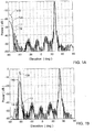
- Fig. 1A illustrates exemplary schematic patterns 11 and 12 of phased array antennas scanned to +40° constituted of linear arrays of identical antenna elements spaced apart at 0.6 ⁇ and having symmetrical and asymmetrical radiation patterns (not shown), respectively.
- a degree of asymmetry of the element radiation patterns is 15°.
- grating lobes 110 and 120 which have correspondingly the levels of -17dB and -23dB, can be observed at -90° on the radiation patterns of the phased array antennas constituted of symmetrical pattern antenna elements and asymmetrical pattern antenna elements, respectively.
- an amplitude of the grating lobe 120 is smaller than the amplitude of the grating lobe 110, owing to the multiplication of the array factor by the asymmetrical radiation pattern of the antenna elements rather than by the symmetrical pattern.
- Fig. 1B illustrates exemplary schematic patterns 13 and 14 for the phased array antennas described above with reference to Fig. 1A , which are scanned now to +50°.
- grating lobes 130 and 140 appear in the visible zone of the radiation patterns at -62°, corresponding to the array antennas constituted of the antenna elements having symmetric and asymmetric radiation patterns, respectively.
- the amplitude level of the grating lobe 130 is -3 dB, while amplitude level of the grating lobe 140 is -17 dB.
- the grating lobe 130 has a relatively significant value that can be sufficient for reducing the operating efficiency of the phased array antenna.
- the amplitude of the grating lobe has a suppressed magnitude.
- the inventors have found that magnitude of the peak of the grating lobes on the resulting array radiation pattern depends on the rate of asymmetry of the single element pattern.
- the single element pattern can be within the range of -50° ⁇ +77° at the level where the gain does not drop from its maximal value greater than 6 dB. It should be understood that such a range can be extended by decreasing the spacing between the antenna elements.
- antenna elements having asymmetrical radiation pattern are not bound by any specific type or configuration of the antenna elements.
- An example of the antenna elements suitable for the purpose of the present invention includes, but is not limited to, the patch antenna element described in U.S. Pat. No. 5,006,857 . As indicated above in the background section, the antenna element disclosed in U.S. Pat. No. 5,006,857 has an asymmetrical shape that results in an asymmetrical element radiation pattern.
- the present invention provides an antenna element having a symmetrical shape, which also produces an asymmetrical element radiation pattern, and thus can be used in an antenna array for suppressing the grating lobes.
- FIG. 2A is a schematic plan view of the antenna element 20
- Fig. 2B is a schematic cross-sectional view of the antenna element 20, taken across the line H-H of Fig. 2A , according to an embodiment of the invention.
- FIG. 2A is a schematic plan view of the antenna element 20
- Fig. 2B is a schematic cross-sectional view of the antenna element 20, taken across the line H-H of Fig. 2A , according to an embodiment of the invention.
- the antenna element 20 includes an "infinite" conductive ground plane 21 having a cavity 22 recessed therein, a radiating patch 23 backed by the cavity 22 and arranged in a cavity aperture 221, and a feed arrangement shown schematically by a reference numeral 24.
- the feed arrangement 24 is coupled to the radiating patch 23 at a feed point 25 located within the patch 23 for providing radio frequency energy thereto.
- the radiating patch 23 is centered in the cavity aperture 221.
- the radiating patch 23 is generally made of conductive material.
- the conductive material suitable for the radiating patch 23 include, but are not limited to, copper, gold and their alloys.
- the radiating patch 23 is selected to be rather thin, such that the patch thickness t is much less than ⁇ ( t ⁇ ⁇ ), where ⁇ is the free-space operating wavelength.
- the conductive ground plane 21 can, for example, be formed from aluminum to provide a lightweight structure, although other materials, e.g., zinc plated steel, can also be employed.
- a plane perpendicular to the radiating patch 23 and passing through a center O of the patch 23 and the feed point 25 defines an electric field plane (E-plane) of the patch antenna element 20, whereas a plane perpendicular to the E-plane and passing through the feed point 25 defines a magnetic field plane (H-plane) of the patch antenna element 20.
- E-plane electric field plane
- H-plane magnetic field plane
- the radiating patch 23 along the E-plane and H-plane are less than the dimensions of the cavity aperture 221.
- the radiating patch 23 has a rectangular shape with the length a along the H-plane and width b along the E-plane.
- the length b can be in the range of about 0.2 to 0.7 ⁇ .
- a shape of the cavity aperture 221 is also rectangular.
- the borders of the cavity aperture 221 are shown by dashed line in Fig. 2A , where the length along the H-plane and width along the E-plane of the cavity aperture 221 are denoted by c and d , respectively.
- the feed point 25 is located at a position apart by a predetermined distance S from the center O of the patch 23 along the E-plane.
- the magnitude of the distance S is such so to provide impedance matching of the antenna element.
- the inventors have found that although the structure of the patch antenna element 20 has a symmetrical shape, nevertheless at certain circumstances the radiation pattern of the antenna element 20 can be asymmetrical.
- a and B determine the character of the radiation pattern produced by the patch antenna element 20. More particularly, the increment B has to be greater than a certain first predetermined value V1 in order that the radiation pattern of the antenna element 20 would be asymmetrical, though the rate of the asymmetry is independent of the value of the increment B . When B ⁇ V1, the radiation pattern remains to be symmetrical. On the other hand, the rate of the asymmetry depends on the value of the increment A . Depending on the requirements, the value of the increment A can always be set to a second predetermined value V2 to achieve a required degree of asymmetry of the element radiating pattern.
- V2 depend on A / ⁇
- V1 depend on B / ⁇
- the wavelength ⁇ 85.65 mm.
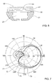
- Fig. 7 and Fig. 8 illustrate a front to back cut of exemplary radiation patterns and a gain-elevation relation, respectively, in E-plane obtained by simulation for the antenna element of the present invention operating at 3.5 GHz.
- the length a of the radiation patch was set to 45 mm.
- the following values of the increment A were selected for the simulation: 2 mm (curves 71 and 81 ), 6 mm (curves 72 and 82 ), 10 mm (curves 73 and 83 ), and 14 mm (curves 74 and 84 ).
- the width b of the radiating patch was set to 29 mm
- the analysis of the radiation properties of antenna element of the present invention at various frequencies has shown that the asymmetrical antenna pattern of the antenna element of the present invention is relatively insensitive to frequency changes, when compared, for example, to the element radiation pattern of the asymmetrical antenna element described in U.S. Pat. No. 5,006,857 .
- the antenna element 20 further includes a dielectric substrate 26 supported on the ground plane 21, which has an outer major side 261 and an inner major side 262.
- the radiating patch 23 is formed on either major side of a dielectric substrate 26, according to the detailed antenna design.
- the radiating patch 23 can be etched on the surface of the dielectric substrate 26 by using a conventional photolithography technique.
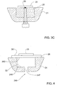
- the radiating patch 23 can be formed on the outer major side 261 (as shown in Fig. 3A ).
- the feed arrangement 24 includes a vertical coaxial line (vertical probe) 245 having an inner conductor 241 and an outer conductor 242.
- the inner conductor 241 is extended through an opening 243 in the conductive ground plane 21, the cavity 22 and an opening 244 in the dielectric substrate 26, and electrically connected to the radiating patch 23 at the feed point 25.
- the outer conductor 242 is connected to the ground plane 21.
- the radiating patch 23 can be formed on the inner major side 262 (as shown in Fig. 3B ).
- the inner conductor 241 of the vertical feed coaxial line is extended through an opening 243 in the conductive ground plane 21 and the cavity 22, and electrically connected to the radiating patch 23 printed on the inner major side 262 at the feed point 25, whereas the outer conductor 242 can be connected to the ground plane 21.
- the cavity 22 recessed in the ground plane 21 is filled with a solid dielectric material having a predetermined dielectric permittivity ⁇ , thereby to form a substrate 263 for supporting the radiating patch 23 thereon.
- the relative dielectric permittivity ⁇ can be in the range of about 1 to 100.
- the inner conductor 241 of the vertical feed coaxial line 245 is extended through an opening 243 in the conductive ground plane 21 and the cavity 22 filled with the dielectric material, and electrically connected to the radiating patch 23 mounted on substrate 263 at the feed point 25, whereas the outer conductor 242 can be connected to the ground plane 21.
- the feed arrangement 24 includes a slot coupled feed line 246 having a coupling slot 247 arranged in the conductive ground plane 21 at a bottom 248 of the cavity 22.
- the radio frequency energy can be provided to the coupling slot 247 by any known manner, for example, the slot coupled feed line 246 can include a waveguide (not shown) or a microstrip line (not shown).
- the amount of non-contacting coupling from the slot coupled feed line 246 to the patch 23 is determined by the shape, size and location of the aperture.
- the coupling slot 247 is rectangular and centered under the rectangular radiating patch, leading to lower cross-polarization due to symmetry of the configuration. It should be understood by a person versed in the art that the invention is compatible also with multislot feed arrangements.
- slots may generally be any shape, such as polygonal, circular and/or elliptical, that provides adequate coupling between the slot coupled feed line 246 and the patch 23.
- the patch 23 is mounted on the outer major side 261 of the dielectric substrate.
- the slot coupled feed line can be provided mutatis mutandis for the antenna configurations when the patch 23 is mounted on the inner major side 262 of the dielectric substrate 26, and for the case when the cavity 22 is filled up with the dielectric material and the patch 23 is mounted on the top thereof.
- the antenna element 20 includes the radiating patch 23, supported on the outer major side 261 of the dielectric substrate 26 and a proximity coupled feed line 51 mounted on the inner major side 262 of the dielectric substrate 26.
- the feed arrangement 24 with the proximity coupled feed line 51 is in the form of a microstrip feed line.
- the radiating patch and the microstrip feed line can be printed by standard techniques onto the dielectric substrate 26, and can, for example, be manufactured in one process.
- the microstrip feed line can be fed from a cable (not shown), and can be of a form such that it provides a suitable matching circuit between the cable and the patch.
- the cable can be a semi-rigid coaxial cable that can be soldered to the microstrip metal, which is typically a copper alloy, at the place under the feed point 25.
- the feed line 51 is connected directly to the radiating patch 23 by means of a plated via 52 or similar.
- Fig. 5B shows an example of how the microstrip feed line formed on one side of the substrate 26 can be connected to the patch 23 arranged on the other side of the substrate 26 by using a via 52.
- the via 52 can, for example, be in the form of an empty bore drilled through the substrate 24 and having a conductive cover on the internal surface of the bore.
- the bores may be filled with a conductive material, e.g. with metal pins.
- electromagnetic field coupling can be used to transfer RF energy between the proximity coupled feed line 51 and the radiating patch 23.
- Fig . 5C shows a cross-sectional view of the antenna element 20 according to still further example, in which the feed arrangement 24 is implemented in the form of a proximity coupled feed line 55.
- the radiating patch 23 is supported on the inner major side 262 of the dielectric substrate 26 whereas the proximity coupled feed line 55 is mounted on the outer major side 261 of the dielectric substrate 26.
- the contacting scheme through a via 52 and non-contacting coupling scheme can be used for feeding the antenna element 20, as described above.
- the antenna element 20 further includes a protection radome 61 for providing environmental protection against moister etc.
- the protection radome 61 is arranged directly on an outer radiating surface 62 of the antenna element. By attaching the radome directly to the antenna, there is no space in which moisture could accumulate. Such moisture would affect the performance of the antenna, both in electrical terms and also in terms of corrosion resistance.
- the protection radome 61 is mounted on the top of the patch 23 when the patch is printed on the outer major side 261 of the dielectric substrate 26.
- the radome 61 can be provided for any kind of feed arrangement 24 and arranged on the outer radiating surface of the antenna mutatis mutandis for the antenna configuration when the patch 23 is mounted on the inner major side 262 of the dielectric substrate 26, and for the case when the cavity 22 is filled up with the dielectric material and the patch 23 is mounted on the top thereof.
- the radome 61 can be manufactured by using a suitable dielectric material, such as glass fibre reinforced plastics and/or ABS plastics. Likewise, the radome 61 can be shaped to conform with the radiating elements and can be colored to provide an aesthetically pleasing cover. This cover can also act as a solar shield to reduce the effects of solar radiation heating and an impact shield to prevent mechanical damage to the base station electronics.
- the construction may further provide environmental sealing for the antenna element to prevent performance degradation of the antenna element during its lifetime due to moisture induced corrosion etc.
- Fig. 9 shows a partial schematic front view of an exemplary phased array antenna 90 comprising a plurality of cavity-backed patch antenna elements 20 of the present invention, and a beam steering system 91 configured for steering an energy beam produced by the phased array antenna 90.
- the patch antenna elements 20 are spaced apart at a predetermined distances L 1 and L2 from each other along system axes x and y , correspondingly.
- the distances L1 and L2 can be equal or different.
- the array antenna 90 can be monolithically co-integrated on-a-chip together with the other elements (e.g., DSP-driven switches of the beam steering system 91 ) and can also radiate steerable multibeams, thus making the whole array a smart antenna.
- the grating lobes which might appear in the visible zone can be suppressed in the entire pattern of the phased array antenna 90.
- the patch antenna element of the present invention may have numerous applications.
- the list of applications includes, but is not limited to, various devices operating in the frequency band of about 100 MHz to 500 GHz.
- the patch antenna element of the present invention would be operative with radars, telemetry stations, jamming stations, communication devices (e.g., mobile phones, PDAs, remote control units, telecommunication with satellites, etc.), etc.
- the antenna of the present invention is not bound to the examples of the rectangular patch and cavity aperture.
- the patch and the cavity aperture may have a different configuration than rectangular. It could be generally polygonal, circular, elliptical or otherwise symmetrical with regard to the center of the patch and cavity aperture.
Landscapes
- Waveguide Aerials (AREA)
- Variable-Direction Aerials And Aerial Arrays (AREA)
Claims (19)
- Phasengesteuerte Gruppenantenne (90), aufweisend mehrere Patch-Antennenelemente (20), die in einem vorgegebenen Abstand, der zwischen λ/2 und λ beträgt, voneinander angeordnet sind, wobei λ eine Betriebswellenlänge der phasengesteuerten Gruppenantenne ist; und ein Strahllenkungssystem (91) zum Lenken eines von der phasengesteuerten Gruppenantenne (90) erzeugten Energiestrahls, wobei das Patch-Antennenelement aufweist:eine leitfähige Massefläche (21), die einen darin ausgesparten Hohlraum (22) hat und eine Hohlraumöffnung (221) begrenzt,ein strahlendes Patch (23), das von dem Hohlraum (22) gestützt wird und in der Hohlraumöffnung angeordnet ist, wobei das strahlende Patch (23) und die Hohlraumöffnung (221) ähnliche symmetrische Formen haben und das strahlende Patch (23) in der Hohlraumöffnung (221) zentriert ist, undeine Speiseanordnung (24), die an einem Speisepunkt (25), der sich in dem Patch (23) in einem vorgegebenen Abstand (S) von einer Mitte des Patch befindet, mit dem strahlenden Patch (23) gekoppelt ist und betreibbar ist, dem Patch Funkfrequenzenergie zuzuführen;dadurch gekennzeichnet, dass das Patch-Antennenelement (20) derart konfiguriert ist, dass(i) eine Größe des strahlenden Patch (23) entlang einer E-Ebene, die als eine zum strahlenden Patch (23) senkrechte und sich durch eine Mitte (O) des Patch (23) und den Speisepunkt (25) erstreckende Ebene definiert ist, um einen ersten vorgegebenen Wert V1 kleiner als die Größe der Hohlraumöffnung (221) entlang der E-Ebene ist;(ii) eine Größe des strahlenden Patch (23) entlang einer H-Ebene, die als eine zur E-Ebene senkrechte und sich durch den Speisepunkt (25) erstreckende Ebene definiert ist, um einen zweiten vorgegebenen Wert V2 kleiner als die Größe der Hohlraumöffnung (221) entlang der H-Ebene ist;wobei der erste und zweite vorgegebene Wert V1, V2 gewählt sind, um ein vorgegebenes asymmetrisches Strahlungsmuster des Patch-Antennenelements bereitzustellen, das eine wesentliche Unterdrückung der Gitterkeulen der phasengesteuerten Gruppenantenne ermöglicht.
- Phasengesteuerte Gruppenantenne (90) nach Anspruch 1, wobei das strahlende Patch (23) und die Hohlraumöffnung (221) symmetrische Formen haben, ausgewählt aus rechteckiger Form, polygonaler Form, Kreisform und elliptischer Form.
- Phasengesteuerte Gruppenantenne (90) nach einem der vorstehenden Ansprüche, wobei eine Dicke des strahlenden Patch (23) kleiner als die Freiraum-Betriebswellenlänge ist.
- Phasengesteuerte Gruppenantenne (90) nach einem der vorstehenden Ansprüche, wobei das strahlende Patch (23) aus einem dielektrischen Substrat (26) gebildet ist, das eine äußere Hauptseite (261) und eine innere Hauptseite (262) hat, wobei die innere Hauptseite (262) der leitfähigen Massefläche (21) zugewandt ist und darauf gelagert ist.
- Phasengesteuerte Gruppenantenne (90) nach Anspruch 4, wobei das strahlende Patch (23) an der äußeren Hauptseite (261) des dielektrischen Substrats (26) gebildet ist.
- Phasengesteuerte Gruppenantenne (90) nach Anspruch 4, wobei das strahlende Patch (23) an der inneren Hauptseite (262) des dielektrischen Substrats (26) gebildet ist.
- Phasengesteuerte Gruppenantenne (90) nach einem der Ansprüche 1 bis 4, wobei der Hohlraum (22) mit einem dielektrischen Material gefüllt ist.
- Phasengesteuerte Gruppenantenne (90) nach Anspruch 7, wobei das dielektrische Material aus einem Feststoff besteht und ein Substrat zum Tragen des strahlenden Patch (23) bildet.
- Phasengesteuerte Gruppenantenne (90) nach Anspruch 1, wobei die Speiseanordnung (24) eine vertikale Koaxialleitung (245) mit einem Innenleiter (241) und einem Außenleiter (242) aufweist, wobei der Innenleiter (241) sich durch eine Öffnung (243) in der leitfähigen Massefläche (21) und den Hohlraum (22) erstreckt und an dem Speisepunkt (25) mit dem strahlenden Patch (23) gekoppelt ist, wohingegen der Außenleiter (242) mit der Massefläche (21) gekoppelt ist.
- Phasengesteuerte Gruppenantenne (90) nach Anspruch 1, wobei die Speiseanordnung (24) eine schlitzgekoppelte Speiseleitung (246) mit mindestens einem Kopplungsschlitz (247) aufweist, der in der leitfähigen Massefläche (21) an einem Boden (248) des Hohlraums (22) angeordnet ist.
- Phasengesteuerte Gruppenantenne (90) nach Anspruch 5, wobei die Speiseanordnung (24) eine proximity-gekoppelte Speiseleitung (51) aufweist.
- Phasengesteuerte Gruppenantenne (90) nach Anspruch 6, wobei die Speiseanordnung (24) eine proximity-gekoppelte Speiseleitung (55) aufweist.
- Phasengesteuerte Gruppenantenne (90) nach Anspruch 11, wobei die proximity-gekoppelte Speiseleitung (51) an der inneren Hauptseite (262) des dielektrischen Substrats (26) angebracht ist.
- Phasengesteuerte Gruppenantenne (90) nach Anspruch 12, wobei die proximity-gekoppelte Speiseleitung (55) an der äußeren Hauptseite (261) des dielektrischen Substrats (26) angebracht ist.
- Phasengesteuerte Gruppenantenne (90) nach Anspruch 11, wobei die proximity-gekoppelte Speiseleitung (51, 55) eine Mikrostreifen-Speiseleitung ist.
- Phasengesteuerte Gruppenantenne (90) nach einem der vorstehenden Ansprüche, wobei sich der Speisepunkt (25) an einer Position befindet, die entlang der E-Ebene in einem vorgegebenen Abstand von der Mitte (O) des strahlenden Patch (23) entfernt ist.
- Phasengesteuerte Gruppenantenne (90) nach einem der vorstehenden Ansprüche, ferner aufweisend ein an einer äußeren strahlenden Oberfläche des Patch-Antennenelements gebildetes Schutzradom (61).
- Verfahren zum Konfigurieren eines symmetrischen Patch-Antennenelements mit einem vorgegebenen asymmetrischen Strahlungsmuster, das eine wesentliche Unterdrückung von Gitterkeulen einer phasengesteuerten Gruppenantenne erlaubt, die mehrere der symmetrischen Patch-Antennenelemente (20) aufweist, die in einem vorgegebenen Abstand, der zwischen λ/2 und λ beträgt, voneinander angeordnet sind, wobei λ eine Betriebswellenlänge der phasengesteuerten Gruppenantenne ist, wobei das Verfahren aufweist:Bereitstellen einer leitfähigen Massefläche (21), die einen darin ausgesparten Hohlraum (22) hat und eine Hohlraumöffnung (221) begrenzt,Bereitstellen eines strahlenden Patch (23), das von dem Hohlraum (22) gestützt wird und in der Hohlraumöffnung angeordnet ist, wobei das strahlende Patch (23) und die Hohlraumöffnung (221) ähnliche symmetrische Formen haben und das strahlende Patch (23) in der Hohlraumöffnung (221) zentriert ist, undBereitstellen einer Speiseanordnung (24), die mit dem strahlenden Patch (23) an einem Speisepunkt (25), der sich in dem Patch (23) in einem vorgegebenen Abstand (S) von einer Mitte des Patch befindet, gekoppelt ist und betreibbar ist, dem Patch Funkfrequenzenergie zuzuführen;Bemessen einer Größe des strahlenden Patch (23) entlang einer E-Ebene, die als eine zum strahlenden Patch (23) senkrechte und sich durch eine Mitte (O) des Patch (23) und den Speisepunkt (25) erstreckende Ebene definiert ist, um einen ersten vorgegebenen Wert V1 kleiner als die Größe der Hohlraumöffnung (221) entlang der E-Ebene;Bemessen einer Größe des strahlenden Patch (23) entlang einer H-Ebene, die als eine zur E-Ebene senkrechte und sich durch den Speisepunkt (25) erstreckende Ebene definiert ist, um einen zweiten vorgegebenen Wert V2 kleiner als die Größe der Hohlraumöffnung (221) entlang der H-Ebene.
- Verfahren zum Unterdrücken von Gitterkeulen, die in einem Strahlungsmuster einer phasengesteuerten Gruppenantenne erzeugt werden, wobei das Verfahren aufweist:Bereitstellen eines symmetrischen Patch-Antennenelements mit einem vorgegebenen asymmetrischen Strahlungsmuster gemäß dem Verfahren nach Anspruch 18, undBilden der phasengesteuerten Gruppenantenne aus mehreren solchen symmetrischen Antennenelementen, die in einem vorgegebenen Abstand, der zwischen λ/2 und λ beträgt, voneinander angeordnet sind, wobei λ eine Betriebswellenlänge der phasengesteuerten Gruppenantenne ist, wobei jedes symmetrische Antennenelement (20) ein asymmetrisches Strahlungsmuster erzeugt, wobei das Verfahren dadurch erlaubt, einen Abtastwinkel eines gelenkten Energiestrahls der phasengesteuerten Gruppenantenne zu erweitern.
Applications Claiming Priority (2)
| Application Number | Priority Date | Filing Date | Title |
|---|---|---|---|
| US11/296,569 US7298333B2 (en) | 2005-12-08 | 2005-12-08 | Patch antenna element and application thereof in a phased array antenna |
| PCT/IL2006/001354 WO2007066322A1 (en) | 2005-12-08 | 2006-11-23 | Patch antenna element and application thereof in a phased array antenna |
Publications (2)
| Publication Number | Publication Date |
|---|---|
| EP1958290A1 EP1958290A1 (de) | 2008-08-20 |
| EP1958290B1 true EP1958290B1 (de) | 2019-03-13 |
Family
ID=37682531
Family Applications (1)
| Application Number | Title | Priority Date | Filing Date |
|---|---|---|---|
| EP06821574.8A Not-in-force EP1958290B1 (de) | 2005-12-08 | 2006-11-23 | Patch-antennenelement und seine anwendung in einer phasengesteuerten gruppenantenne |
Country Status (3)
| Country | Link |
|---|---|
| US (1) | US7298333B2 (de) |
| EP (1) | EP1958290B1 (de) |
| WO (1) | WO2007066322A1 (de) |
Cited By (1)
| Publication number | Priority date | Publication date | Assignee | Title |
|---|---|---|---|---|
| US12620717B2 (en) | 2023-07-14 | 2026-05-05 | Bae Systems Information And Electronic Systems Integration Inc. | Tuning dielectric material in a patch antenna array |
Families Citing this family (32)
| Publication number | Priority date | Publication date | Assignee | Title |
|---|---|---|---|---|
| WO2006051113A1 (en) | 2004-11-12 | 2006-05-18 | Fractus, S.A. | Antenna structure for a wireless device with a ground plane shaped as a loop |
| US20070109197A1 (en) * | 2005-07-15 | 2007-05-17 | M/A-Com, Inc. | Fixed tiltable antenna device |
| FR2915025B1 (fr) * | 2007-04-13 | 2014-02-14 | Centre Nat Etd Spatiales | Antenne a elements rayonnants inclines |
| US7940217B2 (en) * | 2007-08-31 | 2011-05-10 | Et Industries, Inc. | Tree trunk antenna |
| US8812254B2 (en) * | 2009-02-18 | 2014-08-19 | General Electric Company | Methods and systems for monitoring stator winding vibration |
| JPWO2011024722A1 (ja) * | 2009-08-25 | 2013-01-31 | 日本電気株式会社 | アンテナ装置 |
| US8587482B2 (en) * | 2011-01-21 | 2013-11-19 | International Business Machines Corporation | Laminated antenna structures for package applications |
| US8952843B1 (en) * | 2012-03-23 | 2015-02-10 | Rockwell Collins, Inc. | Directional AESA with interferometer direction finding mode |
| JP2013219723A (ja) * | 2012-04-12 | 2013-10-24 | Hitachi Cable Ltd | アンテナ装置 |
| CN104009292B (zh) * | 2014-06-05 | 2016-10-26 | 太原理工大学 | 小型化宽频微带天线 |
| US9823343B2 (en) | 2015-02-27 | 2017-11-21 | Ford Global Technologies, Llc | Digital beamforming based resolution of out-of-path targets showing up as in-path due to grating lobes in array antenna radars |
| CN104953252A (zh) * | 2015-07-01 | 2015-09-30 | 成都众易通科技有限公司 | 相控阵宽角扫描天线单元 |
| CN104953282A (zh) * | 2015-07-01 | 2015-09-30 | 成都众易通科技有限公司 | 相控阵宽角扫描天线系统 |
| CN110622355B (zh) * | 2017-05-30 | 2022-02-11 | 莱森西斯澳大利亚私人有限公司 | 天线 |
| WO2018222556A1 (en) | 2017-06-02 | 2018-12-06 | Flir Systems, Inc. | Ranging systems and methods with staggered multichannel transducers |
| US10656234B2 (en) * | 2017-06-29 | 2020-05-19 | The Boeing Company | Electromagnetic field pattern for phased array antenna |
| CN111801848A (zh) * | 2018-01-05 | 2020-10-20 | 维斯普瑞公司 | 角天线阵列设备、系统和方法 |
| KR102467935B1 (ko) | 2018-04-18 | 2022-11-17 | 삼성전자 주식회사 | 유전체를 포함하는 안테나 모듈 및 이를 포함하는 전자 장치 |
| CN108365335A (zh) * | 2018-05-07 | 2018-08-03 | 南京濠暻通讯科技有限公司 | 一种高增益低剖面微带贴片天线 |
| US11271324B2 (en) * | 2018-07-16 | 2022-03-08 | British Telecommunications Public Limited Company | Cover for a pit |
| US10854986B2 (en) * | 2018-07-18 | 2020-12-01 | Samsung Electro-Mechanics Co., Ltd. | Antenna apparatus |
| CN109066055B (zh) * | 2018-09-28 | 2020-10-20 | 维沃移动通信有限公司 | 一种终端设备 |
| CN109346829B (zh) | 2018-09-28 | 2020-10-02 | 维沃移动通信有限公司 | 一种终端设备 |
| CN109346840B (zh) * | 2018-10-25 | 2021-06-08 | 北京理工大学 | 一种小型天线用低剖面反射口径结构印刷天线 |
| US11867830B2 (en) * | 2019-01-29 | 2024-01-09 | Metawave Corporation | Side lobe reduction in a beam steering vehicle radar antenna for object identification |
| CN110931970B (zh) * | 2019-12-10 | 2021-10-22 | 武汉滨湖电子有限责任公司 | 一种便于调谐的微带贴片天线单元 |
| KR102821236B1 (ko) * | 2019-12-20 | 2025-06-17 | 갭웨이브스 에이비 | 로우-리플 방사 패턴의 안테나 장치 |
| WO2021153035A1 (ja) * | 2020-01-30 | 2021-08-05 | 株式会社村田製作所 | アンテナ装置 |
| CN113065255B (zh) * | 2021-04-07 | 2023-02-17 | 西北工业大学 | 弧度变形的共形微带贴片天线方向图快速估算方法 |
| CN113422202B (zh) * | 2021-06-22 | 2023-09-01 | 维沃移动通信有限公司 | 天线单元和电子设备 |
| CN115241648B (zh) * | 2022-06-27 | 2024-08-06 | 四川大学 | 一种基于mems工艺的悬浮结构空腔贴片天线 |
| IL308374A (en) | 2023-11-07 | 2025-06-01 | Elta Systems Ltd | Dual polarized phasred array antenna |
Family Cites Families (8)
| Publication number | Priority date | Publication date | Assignee | Title |
|---|---|---|---|---|
| US3877031A (en) * | 1973-06-29 | 1975-04-08 | Unied States Of America As Rep | Method and apparatus for suppressing grating lobes in an electronically scanned antenna array |
| US4021812A (en) * | 1975-09-11 | 1977-05-03 | The United States Of America As Represented By The Secretary Of The Air Force | Layered dielectric filter for sidelobe suppression |
| US5006857A (en) * | 1989-08-09 | 1991-04-09 | The Boeing Company | Asymmetrical triangular patch antenna element |
| US5990835A (en) | 1997-07-17 | 1999-11-23 | Northern Telecom Limited | Antenna assembly |
| JPH11231040A (ja) * | 1998-02-12 | 1999-08-27 | Toyota Motor Corp | レーダ装置 |
| US6567048B2 (en) * | 2001-07-26 | 2003-05-20 | E-Tenna Corporation | Reduced weight artificial dielectric antennas and method for providing the same |
| CN100474694C (zh) * | 2004-03-04 | 2009-04-01 | 松下电器产业株式会社 | 单极天线 |
| US7280072B2 (en) * | 2005-04-13 | 2007-10-09 | Brian Mallick | System for the relative navigation of aircraft and spacecraft using a phased array antenna |
-
2005
- 2005-12-08 US US11/296,569 patent/US7298333B2/en not_active Expired - Lifetime
-
2006
- 2006-11-23 EP EP06821574.8A patent/EP1958290B1/de not_active Not-in-force
- 2006-11-23 WO PCT/IL2006/001354 patent/WO2007066322A1/en not_active Ceased
Non-Patent Citations (1)
| Title |
|---|
| GONZALEZ M A ET AL: "Analysis of cavity-backed microstrip antennas by a 3-D finite element/segmentation method and a matrix Lanczos-Pade algorithm (SFELP)", IEEE ANTENNAS AND WIRELESS PROPAGATION LETTERS, IEEE, PISCATAWAY, NJ, US, vol. 1, no. 11, 1 January 2002 (2002-01-01), pages 193 - 195, XP011095577, ISSN: 1536-1225, DOI: 10.1109/LAWP.2002.807783 * |
Cited By (1)
| Publication number | Priority date | Publication date | Assignee | Title |
|---|---|---|---|---|
| US12620717B2 (en) | 2023-07-14 | 2026-05-05 | Bae Systems Information And Electronic Systems Integration Inc. | Tuning dielectric material in a patch antenna array |
Also Published As
| Publication number | Publication date |
|---|---|
| EP1958290A1 (de) | 2008-08-20 |
| US20070132642A1 (en) | 2007-06-14 |
| WO2007066322A1 (en) | 2007-06-14 |
| US7298333B2 (en) | 2007-11-20 |
Similar Documents
| Publication | Publication Date | Title |
|---|---|---|
| EP1958290B1 (de) | Patch-antennenelement und seine anwendung in einer phasengesteuerten gruppenantenne | |
| EP2826097B1 (de) | Phasengesteuerte gruppenantenne | |
| CN106450690B (zh) | 低剖面覆盖式天线 | |
| CA2570658C (en) | Dual polarization antenna array with inter-element coupling and associated methods | |
| EP3375044B1 (de) | Ebg-antenne mit gerichteter fixer strahlrampe | |
| JP6749489B2 (ja) | 単層共用開口デュアルバンドアンテナ | |
| CA2016442A1 (en) | Broadband microstrip-fed antenna | |
| EP3828995B1 (de) | Endgerät | |
| EP3038206B1 (de) | Taper-techniken für augmented e-plane in kontinuierlichen schrägen stummelantennenanordnungen mit variabler neigung | |
| US20130044037A1 (en) | Circuitry-isolated mems antennas: devices and enabling technology | |
| WO2019075190A1 (en) | SYSTEMS, DEVICES AND METHODS FOR LONGITUDINAL RADIATION ANTENNA AND CO-IMPLANTED LOW FREQUENCY ANTENNA | |
| GB2548422B (en) | Antenna array assembly with conductive sidewalls for improved directivity | |
| Noordin et al. | Low-cost antenna array with wide scan angle property | |
| Gupta et al. | A Novel Dielectric Resonator Antenna With Applications in Wide‐Angle Beam‐Scanning Phased Array | |
| Youn et al. | Design of a cylindrical long-slot array antenna integrated with hybrid EBG/ferrite ground plane | |
| Almutawa et al. | Ultrathin planar HIS antenna with beam steering capability for K-band | |
| Li et al. | Compact, low-profile, HIS-based pattern-reconfigurable antenna for wide-angle scanning | |
| JP3045522B2 (ja) | フラッシュマウント・アンテナ | |
| Deng et al. | Single-ridged waveguide antenna for X-band applications | |
| IL191382A (en) | Antenna additive and use in a number of instances of antennas | |
| KR102798772B1 (ko) | S/x 듀얼 대역 레이더를 위한 직교 배열 안테나 | |
| US20250392045A1 (en) | Antenna apparatus | |
| Geng et al. | Millimeter-Wave Dual-Beam Leaky-Wave Antennas for Broadside and Endfire Radiations Based on Hybrid Structures | |
| Liao et al. | Omnidirectional Multibeam Substrate Integrated Horn Array for Unmanned Aerial Vehicles | |
| Gu et al. | Design of a D-Band Tilted Beam Antenna |
Legal Events
| Date | Code | Title | Description |
|---|---|---|---|
| PUAI | Public reference made under article 153(3) epc to a published international application that has entered the european phase |
Free format text: ORIGINAL CODE: 0009012 |
|
| 17P | Request for examination filed |
Effective date: 20080331 |
|
| AK | Designated contracting states |
Kind code of ref document: A1 Designated state(s): AT BE BG CH CY CZ DE DK EE ES FI FR GB GR HU IE IS IT LI LT LU LV MC NL PL PT RO SE SI SK TR |
|
| 17Q | First examination report despatched |
Effective date: 20081104 |
|
| APBK | Appeal reference recorded |
Free format text: ORIGINAL CODE: EPIDOSNREFNE |
|
| APBN | Date of receipt of notice of appeal recorded |
Free format text: ORIGINAL CODE: EPIDOSNNOA2E |
|
| APBR | Date of receipt of statement of grounds of appeal recorded |
Free format text: ORIGINAL CODE: EPIDOSNNOA3E |
|
| DAX | Request for extension of the european patent (deleted) | ||
| APAF | Appeal reference modified |
Free format text: ORIGINAL CODE: EPIDOSCREFNE |
|
| APBT | Appeal procedure closed |
Free format text: ORIGINAL CODE: EPIDOSNNOA9E |
|
| STAA | Information on the status of an ep patent application or granted ep patent |
Free format text: STATUS: EXAMINATION IS IN PROGRESS |
|
| GRAP | Despatch of communication of intention to grant a patent |
Free format text: ORIGINAL CODE: EPIDOSNIGR1 |
|
| STAA | Information on the status of an ep patent application or granted ep patent |
Free format text: STATUS: GRANT OF PATENT IS INTENDED |
|
| INTG | Intention to grant announced |
Effective date: 20181022 |
|
| GRAJ | Information related to disapproval of communication of intention to grant by the applicant or resumption of examination proceedings by the epo deleted |
Free format text: ORIGINAL CODE: EPIDOSDIGR1 |
|
| STAA | Information on the status of an ep patent application or granted ep patent |
Free format text: STATUS: EXAMINATION IS IN PROGRESS |
|
| GRAR | Information related to intention to grant a patent recorded |
Free format text: ORIGINAL CODE: EPIDOSNIGR71 |
|
| GRAS | Grant fee paid |
Free format text: ORIGINAL CODE: EPIDOSNIGR3 |
|
| STAA | Information on the status of an ep patent application or granted ep patent |
Free format text: STATUS: GRANT OF PATENT IS INTENDED |
|
| GRAA | (expected) grant |
Free format text: ORIGINAL CODE: 0009210 |
|
| STAA | Information on the status of an ep patent application or granted ep patent |
Free format text: STATUS: THE PATENT HAS BEEN GRANTED |
|
| INTC | Intention to grant announced (deleted) | ||
| AK | Designated contracting states |
Kind code of ref document: B1 Designated state(s): AT BE BG CH CY CZ DE DK EE ES FI FR GB GR HU IE IS IT LI LT LU LV MC NL PL PT RO SE SI SK TR |
|
| INTG | Intention to grant announced |
Effective date: 20190205 |
|
| REG | Reference to a national code |
Ref country code: GB Ref legal event code: FG4D |
|
| REG | Reference to a national code |
Ref country code: CH Ref legal event code: EP Ref country code: AT Ref legal event code: REF Ref document number: 1108968 Country of ref document: AT Kind code of ref document: T Effective date: 20190315 |
|
| REG | Reference to a national code |
Ref country code: IE Ref legal event code: FG4D |
|
| REG | Reference to a national code |
Ref country code: DE Ref legal event code: R096 Ref document number: 602006057609 Country of ref document: DE |
|
| REG | Reference to a national code |
Ref country code: NL Ref legal event code: MP Effective date: 20190313 |
|
| REG | Reference to a national code |
Ref country code: LT Ref legal event code: MG4D |
|
| PG25 | Lapsed in a contracting state [announced via postgrant information from national office to epo] |
Ref country code: LT Free format text: LAPSE BECAUSE OF FAILURE TO SUBMIT A TRANSLATION OF THE DESCRIPTION OR TO PAY THE FEE WITHIN THE PRESCRIBED TIME-LIMIT Effective date: 20190313 Ref country code: SE Free format text: LAPSE BECAUSE OF FAILURE TO SUBMIT A TRANSLATION OF THE DESCRIPTION OR TO PAY THE FEE WITHIN THE PRESCRIBED TIME-LIMIT Effective date: 20190313 Ref country code: FI Free format text: LAPSE BECAUSE OF FAILURE TO SUBMIT A TRANSLATION OF THE DESCRIPTION OR TO PAY THE FEE WITHIN THE PRESCRIBED TIME-LIMIT Effective date: 20190313 |
|
| PG25 | Lapsed in a contracting state [announced via postgrant information from national office to epo] |
Ref country code: LV Free format text: LAPSE BECAUSE OF FAILURE TO SUBMIT A TRANSLATION OF THE DESCRIPTION OR TO PAY THE FEE WITHIN THE PRESCRIBED TIME-LIMIT Effective date: 20190313 Ref country code: GR Free format text: LAPSE BECAUSE OF FAILURE TO SUBMIT A TRANSLATION OF THE DESCRIPTION OR TO PAY THE FEE WITHIN THE PRESCRIBED TIME-LIMIT Effective date: 20190614 Ref country code: NL Free format text: LAPSE BECAUSE OF FAILURE TO SUBMIT A TRANSLATION OF THE DESCRIPTION OR TO PAY THE FEE WITHIN THE PRESCRIBED TIME-LIMIT Effective date: 20190313 Ref country code: BG Free format text: LAPSE BECAUSE OF FAILURE TO SUBMIT A TRANSLATION OF THE DESCRIPTION OR TO PAY THE FEE WITHIN THE PRESCRIBED TIME-LIMIT Effective date: 20190613 |
|
| REG | Reference to a national code |
Ref country code: AT Ref legal event code: MK05 Ref document number: 1108968 Country of ref document: AT Kind code of ref document: T Effective date: 20190313 |
|
| PG25 | Lapsed in a contracting state [announced via postgrant information from national office to epo] |
Ref country code: ES Free format text: LAPSE BECAUSE OF FAILURE TO SUBMIT A TRANSLATION OF THE DESCRIPTION OR TO PAY THE FEE WITHIN THE PRESCRIBED TIME-LIMIT Effective date: 20190313 Ref country code: EE Free format text: LAPSE BECAUSE OF FAILURE TO SUBMIT A TRANSLATION OF THE DESCRIPTION OR TO PAY THE FEE WITHIN THE PRESCRIBED TIME-LIMIT Effective date: 20190313 Ref country code: IT Free format text: LAPSE BECAUSE OF FAILURE TO SUBMIT A TRANSLATION OF THE DESCRIPTION OR TO PAY THE FEE WITHIN THE PRESCRIBED TIME-LIMIT Effective date: 20190313 Ref country code: PT Free format text: LAPSE BECAUSE OF FAILURE TO SUBMIT A TRANSLATION OF THE DESCRIPTION OR TO PAY THE FEE WITHIN THE PRESCRIBED TIME-LIMIT Effective date: 20190713 Ref country code: CZ Free format text: LAPSE BECAUSE OF FAILURE TO SUBMIT A TRANSLATION OF THE DESCRIPTION OR TO PAY THE FEE WITHIN THE PRESCRIBED TIME-LIMIT Effective date: 20190313 Ref country code: RO Free format text: LAPSE BECAUSE OF FAILURE TO SUBMIT A TRANSLATION OF THE DESCRIPTION OR TO PAY THE FEE WITHIN THE PRESCRIBED TIME-LIMIT Effective date: 20190313 Ref country code: SK Free format text: LAPSE BECAUSE OF FAILURE TO SUBMIT A TRANSLATION OF THE DESCRIPTION OR TO PAY THE FEE WITHIN THE PRESCRIBED TIME-LIMIT Effective date: 20190313 |
|
| PG25 | Lapsed in a contracting state [announced via postgrant information from national office to epo] |
Ref country code: PL Free format text: LAPSE BECAUSE OF FAILURE TO SUBMIT A TRANSLATION OF THE DESCRIPTION OR TO PAY THE FEE WITHIN THE PRESCRIBED TIME-LIMIT Effective date: 20190313 |
|
| REG | Reference to a national code |
Ref country code: DE Ref legal event code: R097 Ref document number: 602006057609 Country of ref document: DE |
|
| PG25 | Lapsed in a contracting state [announced via postgrant information from national office to epo] |
Ref country code: AT Free format text: LAPSE BECAUSE OF FAILURE TO SUBMIT A TRANSLATION OF THE DESCRIPTION OR TO PAY THE FEE WITHIN THE PRESCRIBED TIME-LIMIT Effective date: 20190313 Ref country code: IS Free format text: LAPSE BECAUSE OF FAILURE TO SUBMIT A TRANSLATION OF THE DESCRIPTION OR TO PAY THE FEE WITHIN THE PRESCRIBED TIME-LIMIT Effective date: 20190713 |
|
| PLBE | No opposition filed within time limit |
Free format text: ORIGINAL CODE: 0009261 |
|
| STAA | Information on the status of an ep patent application or granted ep patent |
Free format text: STATUS: NO OPPOSITION FILED WITHIN TIME LIMIT |
|
| PG25 | Lapsed in a contracting state [announced via postgrant information from national office to epo] |
Ref country code: DK Free format text: LAPSE BECAUSE OF FAILURE TO SUBMIT A TRANSLATION OF THE DESCRIPTION OR TO PAY THE FEE WITHIN THE PRESCRIBED TIME-LIMIT Effective date: 20190313 |
|
| 26N | No opposition filed |
Effective date: 20191216 |
|
| PG25 | Lapsed in a contracting state [announced via postgrant information from national office to epo] |
Ref country code: SI Free format text: LAPSE BECAUSE OF FAILURE TO SUBMIT A TRANSLATION OF THE DESCRIPTION OR TO PAY THE FEE WITHIN THE PRESCRIBED TIME-LIMIT Effective date: 20190313 |
|
| PG25 | Lapsed in a contracting state [announced via postgrant information from national office to epo] |
Ref country code: TR Free format text: LAPSE BECAUSE OF FAILURE TO SUBMIT A TRANSLATION OF THE DESCRIPTION OR TO PAY THE FEE WITHIN THE PRESCRIBED TIME-LIMIT Effective date: 20190313 |
|
| REG | Reference to a national code |
Ref country code: CH Ref legal event code: PL |
|
| PG25 | Lapsed in a contracting state [announced via postgrant information from national office to epo] |
Ref country code: LI Free format text: LAPSE BECAUSE OF NON-PAYMENT OF DUE FEES Effective date: 20191130 Ref country code: CH Free format text: LAPSE BECAUSE OF NON-PAYMENT OF DUE FEES Effective date: 20191130 Ref country code: LU Free format text: LAPSE BECAUSE OF NON-PAYMENT OF DUE FEES Effective date: 20191123 Ref country code: MC Free format text: LAPSE BECAUSE OF FAILURE TO SUBMIT A TRANSLATION OF THE DESCRIPTION OR TO PAY THE FEE WITHIN THE PRESCRIBED TIME-LIMIT Effective date: 20190313 |
|
| REG | Reference to a national code |
Ref country code: BE Ref legal event code: MM Effective date: 20191130 |
|
| GBPC | Gb: european patent ceased through non-payment of renewal fee |
Effective date: 20191123 |
|
| PG25 | Lapsed in a contracting state [announced via postgrant information from national office to epo] |
Ref country code: GB Free format text: LAPSE BECAUSE OF NON-PAYMENT OF DUE FEES Effective date: 20191123 Ref country code: IE Free format text: LAPSE BECAUSE OF NON-PAYMENT OF DUE FEES Effective date: 20191123 |
|
| PG25 | Lapsed in a contracting state [announced via postgrant information from national office to epo] |
Ref country code: BE Free format text: LAPSE BECAUSE OF NON-PAYMENT OF DUE FEES Effective date: 20191130 |
|
| PG25 | Lapsed in a contracting state [announced via postgrant information from national office to epo] |
Ref country code: CY Free format text: LAPSE BECAUSE OF FAILURE TO SUBMIT A TRANSLATION OF THE DESCRIPTION OR TO PAY THE FEE WITHIN THE PRESCRIBED TIME-LIMIT Effective date: 20190313 |
|
| PG25 | Lapsed in a contracting state [announced via postgrant information from national office to epo] |
Ref country code: HU Free format text: LAPSE BECAUSE OF FAILURE TO SUBMIT A TRANSLATION OF THE DESCRIPTION OR TO PAY THE FEE WITHIN THE PRESCRIBED TIME-LIMIT; INVALID AB INITIO Effective date: 20061123 |
|
| PGFP | Annual fee paid to national office [announced via postgrant information from national office to epo] |
Ref country code: FR Payment date: 20230929 Year of fee payment: 18 |
|
| PGFP | Annual fee paid to national office [announced via postgrant information from national office to epo] |
Ref country code: DE Payment date: 20230926 Year of fee payment: 18 |
|
| REG | Reference to a national code |
Ref country code: DE Ref legal event code: R119 Ref document number: 602006057609 Country of ref document: DE |
|
| PG25 | Lapsed in a contracting state [announced via postgrant information from national office to epo] |
Ref country code: DE Free format text: LAPSE BECAUSE OF NON-PAYMENT OF DUE FEES Effective date: 20250603 |
|
| PG25 | Lapsed in a contracting state [announced via postgrant information from national office to epo] |
Ref country code: FR Free format text: LAPSE BECAUSE OF NON-PAYMENT OF DUE FEES Effective date: 20241130 |