EP1959527B1 - Laseranordnung und Halbleiterlaser zum optischen Pumpen eines Lasers - Google Patents
Laseranordnung und Halbleiterlaser zum optischen Pumpen eines Lasers Download PDFInfo
- Publication number
- EP1959527B1 EP1959527B1 EP07016309.2A EP07016309A EP1959527B1 EP 1959527 B1 EP1959527 B1 EP 1959527B1 EP 07016309 A EP07016309 A EP 07016309A EP 1959527 B1 EP1959527 B1 EP 1959527B1
- Authority
- EP
- European Patent Office
- Prior art keywords
- laser
- semiconductor
- active
- pump radiation
- optically pumped
- Prior art date
- Legal status (The legal status is an assumption and is not a legal conclusion. Google has not performed a legal analysis and makes no representation as to the accuracy of the status listed.)
- Not-in-force
Links
Images

Classifications
-
- H—ELECTRICITY
- H01—ELECTRIC ELEMENTS
- H01S—DEVICES USING THE PROCESS OF LIGHT AMPLIFICATION BY STIMULATED EMISSION OF RADIATION [LASER] TO AMPLIFY OR GENERATE LIGHT; DEVICES USING STIMULATED EMISSION OF ELECTROMAGNETIC RADIATION IN WAVE RANGES OTHER THAN OPTICAL
- H01S5/00—Semiconductor lasers
- H01S5/40—Arrangement of two or more semiconductor lasers, not provided for in groups H01S5/02 - H01S5/30
- H01S5/4025—Array arrangements, e.g. constituted by discrete laser diodes or laser bar
- H01S5/4031—Edge-emitting structures
- H01S5/4043—Edge-emitting structures with vertically stacked active layers
-
- B—PERFORMING OPERATIONS; TRANSPORTING
- B82—NANOTECHNOLOGY
- B82Y—SPECIFIC USES OR APPLICATIONS OF NANOSTRUCTURES; MEASUREMENT OR ANALYSIS OF NANOSTRUCTURES; MANUFACTURE OR TREATMENT OF NANOSTRUCTURES
- B82Y20/00—Nanooptics, e.g. quantum optics or photonic crystals
-
- H—ELECTRICITY
- H01—ELECTRIC ELEMENTS
- H01S—DEVICES USING THE PROCESS OF LIGHT AMPLIFICATION BY STIMULATED EMISSION OF RADIATION [LASER] TO AMPLIFY OR GENERATE LIGHT; DEVICES USING STIMULATED EMISSION OF ELECTROMAGNETIC RADIATION IN WAVE RANGES OTHER THAN OPTICAL
- H01S3/00—Lasers, i.e. devices using stimulated emission of electromagnetic radiation in the infrared, visible or ultraviolet wave range
- H01S3/05—Construction or shape of optical resonators; Accommodation of active medium therein; Shape of active medium
- H01S3/06—Construction or shape of active medium
- H01S3/0602—Crystal lasers or glass lasers
- H01S3/0604—Crystal lasers or glass lasers in the form of a plate or disc
-
- H—ELECTRICITY
- H01—ELECTRIC ELEMENTS
- H01S—DEVICES USING THE PROCESS OF LIGHT AMPLIFICATION BY STIMULATED EMISSION OF RADIATION [LASER] TO AMPLIFY OR GENERATE LIGHT; DEVICES USING STIMULATED EMISSION OF ELECTROMAGNETIC RADIATION IN WAVE RANGES OTHER THAN OPTICAL
- H01S3/00—Lasers, i.e. devices using stimulated emission of electromagnetic radiation in the infrared, visible or ultraviolet wave range
- H01S3/05—Construction or shape of optical resonators; Accommodation of active medium therein; Shape of active medium
- H01S3/06—Construction or shape of active medium
- H01S3/063—Waveguide lasers, i.e. whereby the dimensions of the waveguide are of the order of the light wavelength
- H01S3/067—Fibre lasers
-
- H—ELECTRICITY
- H01—ELECTRIC ELEMENTS
- H01S—DEVICES USING THE PROCESS OF LIGHT AMPLIFICATION BY STIMULATED EMISSION OF RADIATION [LASER] TO AMPLIFY OR GENERATE LIGHT; DEVICES USING STIMULATED EMISSION OF ELECTROMAGNETIC RADIATION IN WAVE RANGES OTHER THAN OPTICAL
- H01S3/00—Lasers, i.e. devices using stimulated emission of electromagnetic radiation in the infrared, visible or ultraviolet wave range
- H01S3/09—Processes or apparatus for excitation, e.g. pumping
- H01S3/091—Processes or apparatus for excitation, e.g. pumping using optical pumping
- H01S3/094—Processes or apparatus for excitation, e.g. pumping using optical pumping by coherent light
- H01S3/094096—Multi-wavelength pumping
-
- H—ELECTRICITY
- H01—ELECTRIC ELEMENTS
- H01S—DEVICES USING THE PROCESS OF LIGHT AMPLIFICATION BY STIMULATED EMISSION OF RADIATION [LASER] TO AMPLIFY OR GENERATE LIGHT; DEVICES USING STIMULATED EMISSION OF ELECTROMAGNETIC RADIATION IN WAVE RANGES OTHER THAN OPTICAL
- H01S3/00—Lasers, i.e. devices using stimulated emission of electromagnetic radiation in the infrared, visible or ultraviolet wave range
- H01S3/09—Processes or apparatus for excitation, e.g. pumping
- H01S3/091—Processes or apparatus for excitation, e.g. pumping using optical pumping
- H01S3/094—Processes or apparatus for excitation, e.g. pumping using optical pumping by coherent light
- H01S3/0941—Processes or apparatus for excitation, e.g. pumping using optical pumping by coherent light of a laser diode
-
- H—ELECTRICITY
- H01—ELECTRIC ELEMENTS
- H01S—DEVICES USING THE PROCESS OF LIGHT AMPLIFICATION BY STIMULATED EMISSION OF RADIATION [LASER] TO AMPLIFY OR GENERATE LIGHT; DEVICES USING STIMULATED EMISSION OF ELECTROMAGNETIC RADIATION IN WAVE RANGES OTHER THAN OPTICAL
- H01S3/00—Lasers, i.e. devices using stimulated emission of electromagnetic radiation in the infrared, visible or ultraviolet wave range
- H01S3/09—Processes or apparatus for excitation, e.g. pumping
- H01S3/091—Processes or apparatus for excitation, e.g. pumping using optical pumping
- H01S3/094—Processes or apparatus for excitation, e.g. pumping using optical pumping by coherent light
- H01S3/0941—Processes or apparatus for excitation, e.g. pumping using optical pumping by coherent light of a laser diode
- H01S3/09415—Processes or apparatus for excitation, e.g. pumping using optical pumping by coherent light of a laser diode the pumping beam being parallel to the lasing mode of the pumped medium, e.g. end-pumping
-
- H—ELECTRICITY
- H01—ELECTRIC ELEMENTS
- H01S—DEVICES USING THE PROCESS OF LIGHT AMPLIFICATION BY STIMULATED EMISSION OF RADIATION [LASER] TO AMPLIFY OR GENERATE LIGHT; DEVICES USING STIMULATED EMISSION OF ELECTROMAGNETIC RADIATION IN WAVE RANGES OTHER THAN OPTICAL
- H01S5/00—Semiconductor lasers
- H01S5/30—Structure or shape of the active region; Materials used for the active region
- H01S5/305—Structure or shape of the active region; Materials used for the active region characterised by the doping materials used in the laser structure
- H01S5/3095—Tunnel junction
-
- H—ELECTRICITY
- H01—ELECTRIC ELEMENTS
- H01S—DEVICES USING THE PROCESS OF LIGHT AMPLIFICATION BY STIMULATED EMISSION OF RADIATION [LASER] TO AMPLIFY OR GENERATE LIGHT; DEVICES USING STIMULATED EMISSION OF ELECTROMAGNETIC RADIATION IN WAVE RANGES OTHER THAN OPTICAL
- H01S5/00—Semiconductor lasers
- H01S5/30—Structure or shape of the active region; Materials used for the active region
- H01S5/34—Structure or shape of the active region; Materials used for the active region comprising quantum well or superlattice structures, e.g. single quantum well [SQW] lasers, multiple quantum well [MQW] lasers or graded index separate confinement heterostructure [GRINSCH] lasers
- H01S5/343—Structure or shape of the active region; Materials used for the active region comprising quantum well or superlattice structures, e.g. single quantum well [SQW] lasers, multiple quantum well [MQW] lasers or graded index separate confinement heterostructure [GRINSCH] lasers in AIIIBV compounds, e.g. AlGaAs-laser, InP-based laser
-
- H—ELECTRICITY
- H01—ELECTRIC ELEMENTS
- H01S—DEVICES USING THE PROCESS OF LIGHT AMPLIFICATION BY STIMULATED EMISSION OF RADIATION [LASER] TO AMPLIFY OR GENERATE LIGHT; DEVICES USING STIMULATED EMISSION OF ELECTROMAGNETIC RADIATION IN WAVE RANGES OTHER THAN OPTICAL
- H01S5/00—Semiconductor lasers
- H01S5/40—Arrangement of two or more semiconductor lasers, not provided for in groups H01S5/02 - H01S5/30
- H01S5/4018—Lasers electrically in series
-
- H—ELECTRICITY
- H01—ELECTRIC ELEMENTS
- H01S—DEVICES USING THE PROCESS OF LIGHT AMPLIFICATION BY STIMULATED EMISSION OF RADIATION [LASER] TO AMPLIFY OR GENERATE LIGHT; DEVICES USING STIMULATED EMISSION OF ELECTROMAGNETIC RADIATION IN WAVE RANGES OTHER THAN OPTICAL
- H01S5/00—Semiconductor lasers
- H01S5/40—Arrangement of two or more semiconductor lasers, not provided for in groups H01S5/02 - H01S5/30
- H01S5/4025—Array arrangements, e.g. constituted by discrete laser diodes or laser bar
- H01S5/4087—Array arrangements, e.g. constituted by discrete laser diodes or laser bar emitting more than one wavelength
Definitions
- the invention relates to a laser arrangement according to the preamble of patent claim 1.
- the optical pumping of a laser in particular of a solid-state laser, can be carried out, for example, by flash lamps or by a further laser, which is referred to as a pump laser.
- a pump laser in particular a comparatively inexpensive semiconductor laser can be used.
- this increases the production cost of the laser assembly from the optically pumped laser and the pump lasers.
- the absorption capacity of an absorption band of the laser to be pumped is limited by the volume of the light-absorbing medium and therefore saturable.
- increasing the pump power in the region of saturation no longer leads to an increase in the output power of the optically pumped laser.
- the saturation threshold of the optically pumped laser can be increased by increasing the volume of the laser-active medium, thereby But also increase the size and cost of the laser adversely.
- semiconductor lasers which have a monolithically integrated laser diode stack with a plurality of active zones, which are arranged one above the other on a common substrate.
- a semiconductor laser is for example from the document WO 99/39405 known.
- the publication US 6,101,208 discloses a pumping arrangement for a laser rod in which the laser rod is pumped with orthogonally arranged laser diodes to uniformly pump the center of the laser rod with high pumping power.
- the invention is based on the object, an improved laser assembly of an optically pumped laser and Specify semiconductor lasers for optical pumping of the laser, which is characterized in particular by an improved efficiency of optical pumping, the size and the production cost of the laser array are relatively small.
- the semiconductor lasers comprise a plurality of monolithically integrated stacked active zones, at least two of the plurality of active zones emitting pump radiation of different wavelengths.
- the different wavelengths of the pump radiation are each suitable for optically pumping different absorption bands of an active medium of the optically pumped laser.
- the one of the first and the second semiconductor laser reaches the active medium in the inventive laser arrangement of two substantially perpendicular directions of incidence.
- At least one of the active zones arranged one above the other within a layer stack of semiconductor lasers emits pump radiation having a wavelength ⁇ 1 and at least one further active zone pump radiation having a wavelength ⁇ 2 , where ⁇ 1 ⁇ ⁇ 2 .
- the semiconductor lasers acting as pumping radiation sources emit pumping radiation of different wavelengths, advantageously several absorption bands of the optically pumped one are obtained Lasers pumped at the same time. This is advantageous in particular when the pump radiation of a first wavelength emitted by an active zone is already sufficient to pump an absorption band of the optically pumped laser into a region of saturation.
- pump radiation having a second wavelength emitted by at least one further active zone
- pump radiation is advantageously radiated into an active medium of the optically pumped laser, which is absorbed in a further absorption band.
- the effective pump power can be increased without increasing the volume of the active medium of the optically pumped laser. It is therefore advantageous if the different wavelengths of the pump radiation are adapted to different absorption bands of the optically pumped laser.
- the optically pumped laser is preferably a solid-state laser.
- the active medium of the optically pumped laser may have various geometric shapes, in particular it may be a rod, a disk or a fiber.
- the material of the active medium of the optically pumped laser may be any material suitable as an active medium of a laser.
- the active medium may be Nd: YAG, Nd: YVO 4, Nd: YAlO 3, Nd: sapphire contain: YLF, Yb: YAG or Ti.
- the number of the plurality of active regions of the semiconductor lasers is preferably between two and ten, inclusive.
- the semiconductor lasers have three or more active regions with which three or more absorption bands of the optically pumped Lasers are pumped.
- a plurality of the active zones of the semiconductor lasers can have the same emission wavelength in order to achieve the greatest possible pumping power at this wavelength.
- the semiconductor lasers contain at least one further active zone which emits at a different wavelength.
- a resonator length of the semiconductor laser is preferably between 0.3 mm and 10 mm.
- the resonator length is given in the semiconductor laser, for example, by the distance of the resonator forming side edges of the edge emitting semiconductor laser.
- a difference between the smallest and the largest of the different wavelengths of the pump radiation is 200 nm or less.
- the active zones of the semiconductor lasers preferably each have a quantum well structure.
- the quantum well structure may be a single quantum well structure or a multiple quantum well structure.
- the term quantum well structure encompasses any structure in which charge carriers undergo quantization of their energy states by confinement.
- the term quantum well structure does not include information about the dimensionality of the quantization. It thus includes quantum wells, quantum wires and quantum dots and any combination of these structures.
- the different emission wavelengths of the plurality of active zones can be realized, in particular, in that the single or multiple quantum well structures of the several active zones differ in their layer thicknesses and / or their material compositions from each other. Alternatively, it is also possible that the dimension of the quantization of the charge carriers in the several active zones differs from each other. For example, one of the plurality of active zones may have quantum dots while another active zone has quantum wells.
- the laser arrangement includes a plurality of semiconductor lasers for optically pumping the optically pumped laser, each having a plurality of monolithically integrated active zones. This is particularly advantageous when the optically pumped laser is a high power laser requiring a high pump power that can not be readily realized with a single semiconductor laser despite the monolithic integration of multiple active regions in the semiconductor laser.
- the number of the semiconductor lasers is preferably between two and two hundred, inclusive.
- the different wavelengths of the pump radiation are advantageously suitable for optically pumping different absorption bands of an active medium to be pumped.
- the semiconductor lasers may be adapted to pump an active medium containing Nd: YAG, Yb: YAG or Ti: sapphire.
- the difference between the The smallest and the largest of the different wavelengths of the pump radiation is preferably 200 nm or less.
- the active zones of the semiconductor lasers preferably each have a single or multiple quantum well structure, with the quantum well structures of the several active zones advantageously differing in their layer thicknesses and / or their material compositions from one another.
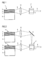
- the illustrated laser arrangement includes an optically pumped laser 2 which emits laser radiation 8.
- the laser arrangement contains a semiconductor laser 1 which emits pump radiation 6.
- dashed lines indicate the envelope of the pump radiation field.
- the pump radiation 6 is focused, for example, by means of a lens 10 into the active medium 7 of the laser 2.
- other optical elements or combinations of optical elements such as lens combinations, mirrors, diffraction gratings or optical fibers for deflecting and / or focusing the pump radiation 6 may be provided in the active medium 7 of the laser 2.
- the semiconductor laser 1 includes a plurality of active zones 3, 4, 5, which are arranged monolithically integrated one above the other in the semiconductor laser 1.
- the plurality of active zones 3, 4, 5 can be connected to each other, for example, in a semiconductor layer sequence applied to a substrate 9 by tunnel junctions (not shown).
- the substrate 9 of the semiconductor laser 1 is, for example, a GaAs substrate.
- the plurality of active zones 3, 4, 5 emit pump radiation 6 for optically pumping the laser 2, the wavelengths of the emitted pump radiation 6 being different from each other in at least two of the active zones.
- one of the plurality of active zones 3, 4, 5, for example the middle active zone 4 emit radiation of a first wavelength ⁇ 1
- the two remaining active zones, for example the outer active zones 3, 5, emit pump radiation 6 with a second wavelength ⁇ 2 emit, where ⁇ 1 ⁇ ⁇ 2 .
- each of the active zones 3, 4, 5 can also emit pump radiation having a wavelength which is different from the wavelengths of the pump radiation emitted by the remaining active zones.
- the upper active zone 3 emits pump radiation having a wavelength ⁇ 1
- the middle active zone 4 emits pump radiation having a wavelength ⁇ 2
- the lower active zone 5 emits pump radiation having a wavelength ⁇ 3 .
- the semiconductor laser 1 emits pump radiation 6 having different wavelengths, advantageously several absorption bands of the active medium 7 of the optically pumped laser 2 can be pumped simultaneously with a single semiconductor laser.
- the wavelengths emitted by the plurality of active zones are advantageously selected such that they are capable of being absorbed in different absorption bands of the active medium 7.
- the active medium 7 of the optically pumped laser 2 can have various geometric shapes, in particular the optically pumped laser 2 can be a disk laser, a bar laser or a fiber laser.
- the optically pumped laser 2 is a solid-state laser.
- This may contain as active medium 7 in particular Nd: YAG, Yb: YAG or Ti: sapphire.
- active medium 7 in particular Nd: YAG, Yb: YAG or Ti: sapphire.
- another laser medium having a plurality of absorption bands suitable for optical pumping may also be used.
- the optical pumping of several absorption bands in the active medium 7 of the optically pumped laser 2 is particularly advantageous when a first absorption band of the active medium 7 has already been pumped into a region of saturation. In this case, an increase in the pumping power would not easily lead to an increase in the output power of the laser radiation 8 emitted by the optically pumped laser 2.
- By injecting pump radiation 6 into at least one further absorption band of the active medium 7 of the optically pumped laser 2 further electrons can advantageously be raised to an upper laser level of the optically pumped laser 2.
- the pumping power absorbed by the optically pumped laser 2 can advantageously be increased without increasing the volume of the active medium 7.
- An optically pumped laser 2 pumped with pump radiation 6 having multiple wavelengths may thus be smaller for the same pump power than a comparable laser pumped at only a single wavelength.
- a further increase in the pump power is advantageously achieved by using a plurality of semiconductor lasers instead of a single semiconductor laser 1 for optically pumping the laser 2.
- an optically pumped laser 2 is optically pumped by a first semiconductor laser 1a and a second semiconductor laser 1b.
- the embodiment and the advantageous embodiments of the semiconductor lasers 1a and 1b correspond to the example described above, ie in particular the semiconductor lasers 1a and 1b each have a plurality of pump radiation emitting active zones 3, 4, 5, wherein the wavelengths of the emitted pump radiation in at least two of the active zones 3, 4, 5 differ from each other.
- the pump radiation 6 emitted by the semiconductor laser 1a is focused into the active medium 7 of the optically pumped laser 2 by means of a combination of a lens 10 and a mirror 11. Furthermore, the pump radiation 6 emitted by the second semiconductor laser 1b is focused with another lens 10 into the active medium 7 of the optically pumped laser.
- the pump radiation 6 advantageously reaches the active medium 7 in this exemplary embodiment from two directions of incidence which are substantially perpendicular to one another, whereby the homogeneity of the optical pumping of the active medium 7 is advantageously improved.
- the laser arrangement preferably includes between two and including two hundred semiconductor lasers 1a, 1b.
- any desired optical elements can be used for beam guidance of the pump radiation 6 emitted by the semiconductor lasers 1a, 1b to the active medium 7 of the optically pumped laser 2, for example lenses, mirrors, diffraction gratings, light guides or combinations of such elements.
- the optically pumped laser 2 is a fiber laser, in which the active medium 7 by a fiber 12th is formed.
- the fiber laser 2 is pumped by a semiconductor laser 1, which contains a plurality of active zones 3, 4, 5, wherein at least two of the plurality of active zones 3, 4, 5 emit pump radiation 6 with different wavelengths.
- the different wavelengths of the pump radiation 6 are advantageously adapted to different absorption bands of the fiber.
- the pumping radiation 6 is preferably focused by means of a lens 10 or other optical elements in one end of the fiber 12.
- the laser radiation 8 of the laser 2 is emitted, for example, from the opposite end of the fiber 12.
- the third example of a laser arrangement corresponds to the first example described above.
- FIG. 4 For example, a semiconductor laser 1 according to an example is shown schematically in cross-section.
- the advantageous embodiments of the semiconductor laser 1 explained below with reference to this example also apply to the previously described embodiments FIGS. 1 to 3 illustrated semiconductor laser.
- the semiconductor laser 1 comprises a semiconductor layer sequence 20 applied to a substrate 9, which comprises a plurality of monolithically integrated laser diodes, for example three laser diodes 17, 18, 19.
- the laser diodes 17, 18, 19 are preferably interconnected by tunnel junctions 15.
- Each of the laser diodes 17, 18, 19 contains an active zone 3, 4, 5 from which radiation 6 is emitted.
- the of the a plurality of active zones 3, 4, 5 emitted radiation 6 is provided for pumping an optically pumped laser.
- At least two of the plurality of active zones 3, 4, 5 emit pump radiation 6 whose wavelength differs from one another.
- the uppermost active layer 3 arranged in the semiconductor layer sequence 20 emits pump radiation 6 with a wavelength ⁇ 1
- an average active layer 4 arranged in the semiconductor layer sequence 20 pump radiation 6 having a wavelength ⁇ 2 and a lower active layer 5 arranged in the semiconductor layer sequence 20 with a wavelength ⁇ 3 .
- the wavelengths ⁇ 1 , ⁇ 2 and ⁇ 3 advantageously correspond to the absorption bands of an optically pumped laser, which is to be pumped by the semiconductor laser 1.
- the semiconductor laser 1 may be suitable for optically pumping a solid-state laser, wherein the solid-state laser may contain, for example, Nd: YAG, Yb: YAG or Ti: sapphire as the active medium.
- the active zones 3, 4, 5 differ from each other, for example, in their material and / or their layer thicknesses.
- the active zones 3, 4, 5 each contain a quantum well structure.
- the laser threshold is comparatively low compared to a semiconductor laser with a conventional pn junction as the active zone. Furthermore, in this case, the temperature dependence of the emission wavelengths is advantageously low.
- the quantum well structures of the plurality of active zones 3, 4, 5 may differ in their material composition and / or their layer thicknesses in order to obtain different emission wavelengths ⁇ 1 , ⁇ 2 and ⁇ 3 .
- the quantum well structures differ from one another in the dimensionality of the quantization.
- one of the quantum well structures can contain quantum dots, while at least one of the further quantum well structures contains quantum wells or quantum wires.
- the wavelength difference between the shortest of the emitted wavelengths ⁇ 1 , ⁇ 2 and ⁇ 3 and the longest emitted wavelength is preferably 200 nm or less.
- three active zones 3, 4, 5 are arranged in the semiconductor laser 1.
- a different number of active zones is conceivable, with preferably between two and including ten active zones in the semiconductor laser 1 are arranged.
- the active zones 3, 4, 5 are preferably embedded in waveguide layers 13, wherein the waveguide layers 13 are surrounded by cladding layers 14. Between the waveguide layers 13 and the cladding layers 14, there is advantageously such a refractive index difference that the laser radiation is guided in the waveguide 13.
- the thicknesses and material compositions of waveguide layers 13 and / or cladding layers 14 need not be in all Laser diodes 17, 18, 19 be the same, but may also differ from each other.
- the laser resonator of the semiconductor laser 1 is formed, for example, by the side flanks 21, 22 of the semiconductor layer sequence 20.
- An at least partial reflection of the laser radiation generated in the active zones 3, 4, 5 on the side flanks 21, 22 takes place, for example, due to the refractive index jump between the material of the semiconductor layer sequence 20 and the surrounding medium, for example air.
- the side flanks 21, 22 of the semiconductor laser 1 may also be provided with a reflection-enhancing coating (not shown).
- the length L of the laser resonator is between 0.3 mm inclusive and 10 mm inclusive.
- the electrical contacting of the semiconductor laser 1 can take place, for example, by using a conductive substrate 9, which represents a first electrical contact of the semiconductor layer sequence 20.
- a second electrical contact of the semiconductor layer sequence 20 is formed, for example, by a contact layer 16 which is applied to a surface of the semiconductor layer sequence 20 lying opposite the substrate 9.
- the semiconductor layer sequence 20 of the semiconductor laser 1 is preferably based on a III-V compound semiconductor material, in particular on an arsenide, nitride or phosphide compound semiconductor material.
- the semiconductor layer sequence 20 In x Al y Ga 1-xy N, In x Al y Ga 1-xy P or In x Al y Ga 1-xy As, each with 0 ⁇ x ⁇ 1, 0 ⁇ y ⁇ 1 and x + y ⁇ 1.
- the III-V compound semiconductor material does not necessarily have to have a mathematically exact composition according to one of the above formulas. Rather, it may have one or more dopants as well as additional ingredients that do not substantially alter the physical properties of the material.
- the above formulas contain only the essential constituents of the crystal lattice, even if these may be partially replaced by small amounts of other substances.
- the material selection for the semiconductor layer sequence 20 is based on the desired emission wavelengths of the semiconductor laser 1.
- the substrate 9 is selected based on the epitaxially preferably grown semiconductor layer sequence 20 and may be in particular a GaAs, GaN, SiC or a silicon substrate.
Landscapes
- Physics & Mathematics (AREA)
- Nanotechnology (AREA)
- Engineering & Computer Science (AREA)
- Chemical & Material Sciences (AREA)
- Optics & Photonics (AREA)
- Biophysics (AREA)
- Life Sciences & Earth Sciences (AREA)
- Electromagnetism (AREA)
- General Physics & Mathematics (AREA)
- Crystallography & Structural Chemistry (AREA)
- Condensed Matter Physics & Semiconductors (AREA)
- Semiconductor Lasers (AREA)
- Lasers (AREA)
Description
- Die Erfindung betrifft eine Laseranordnung gemäß dem Oberbegriff des Patentanspruchs 1.
- Diese Patentanmeldung beansprucht die Priorität der deutschen Patentanmeldungen
10 2006 059 700.1 und10 2006 046 035.9 . - Das optische Pumpen eines Lasers, insbesondere eines Festkörperlasers, kann beispielsweise durch Blitzlampen oder durch einen weiteren Laser, der als Pumplaser bezeichnet wird, erfolgen. Als Pumplaser kann insbesondere ein vergleichsweise kostengünstiger Halbleiterlaser eingesetzt werden. Um die Pumpleistung und damit die Ausgangsleistung des optisch gepumpten Lasers zu erhöhen, ist es möglich, mehrere Halbleiterlaser zum optischen Pumpen eines optisch gepumpten Lasers einzusetzen. Dadurch erhöht sich aber der Herstellungsaufwand der Laseranordnung aus dem optisch gepumpten Laser und den Pumplasern.
- Das Absorptionsvermögen einer Absorptionsbande des zu pumpenden Lasers ist durch das Volumen des lichtabsorbierenden Mediums begrenzt und deshalb sättigbar. Somit führt eine Erhöhung der Pumpleistung im Bereich der Sättigung nicht mehr zu einer Erhöhung der Ausgangsleistung des optisch gepumpten Lasers. Die Sättigungsschwelle des optisch gepumpten Lasers kann zwar durch eine Vergrößerung des Volumens des laseraktiven Mediums erhöht werden, wodurch sich aber auch die Baugröße und die Herstellungskosten des Lasers nachteilig erhöhen.
- Zur Erzielung einer hohen Strahlungsleistung mit einem einzelnen Halbleiterlaser sind Halbleiterlaser bekannt, die einen monolithisch integrierten Laserdiodenstapel mit mehreren aktiven Zonen aufweisen, die auf einem gemeinsamen Substrat übereinander angeordnet sind. Ein derartiger Halbleiterlaser ist beispielsweise aus der Druckschrift
WO 99/39405 US 5,212,706 ein kantenemittierender Halbleiterlaser beschrieben, bei dem mehrere Laserdioden monolithisch übereinander abgeschieden sind und die Laserdioden mittels Tunnelübergängen miteinander verbunden sind. - In der Druckschrift
US 4,901,330 wird ein optisch gepumpter Laser beschrieben, bei dem zum optischen Pumpen eine Laserdiode mit mehreren übereinander angeordneten aktiven Zonen verwendet wird. Es wird beschrieben, dass die mehreren aktiven Zonen verschiedene Wellenlängen aufweisen können, um eine vergrößerte Bandbreite der Pumpstrahlung zu erzielen. Auf diese Weise wird Pumpstrahlung mit einer Bandbreite von etwa 3 nm bis 15 nm generiert, um ein Absorptionsband des optisch gepumpten Lasers innerhalb dieser Bandbreite optisch zu pumpen. - Die Druckschrift
US 6,101,208 offenbart eine Pumpanordnung für einen Laserstab, bei der der Laserstab mit orthogonal angeordneten Laserdioden gepumpt wird, um das das Zentrum des Laserstabs gleichmäßig mit hoher Pumpleistung zu pumpen. - Der Erfindung liegt die Aufgabe zugrunde, eine verbesserte Laseranordnung aus einem optisch gepumpten Laser und Halbleiterlasern zum optischen Pumpen des Lasers anzugeben, die sich insbesondere durch eine verbesserte Effizienz des optischen Pumpens auszeichnet, wobei die Baugröße und der Herstellungsaufwand der Laseranordnung vergleichsweise gering sind.
- Diese Aufgabe wird durch eine Laseranordnung gemäß Patentanspruch 1 gelöst. Vorteilhafte Ausgestaltungen und Weiterbildungen der Erfindung sind Gegenstand der abhängigen Ansprüche.
- Bei einer erfindungsgemäßen Laseranordnung aus einem optisch gepumpten Laser und mindestens zwei Halbleiterlasern, die Pumpstrahlung zum Pumpen des optisch gepumpten Lasers emittieren, enthalten die Halbleiterlaser mehrere monolithisch integrierte übereinander angeordnete aktive Zonen, wobei mindestens zwei der mehreren aktiven Zonen Pumpstrahlung verschiedener Wellenlängen emittieren. Die verschiedenen Wellenlängen der Pumpstrahlung sind jeweils zum optischen Pumpen verschiedener Absorptionsbanden eines aktiven Mediums des optisch gepumpten Lasers geeignet. Die des ersten und des zweiten Halbleiterlasers erreicht das aktive Medium bei dem erfindungsgemässen Laseranordnung aus zwei im Wesentlichen senkrecht zueinander stehenden Einfallsrichtungen.
- Mindestens eine der innerhalb eines Schichtstapels der Halbleiterlaser übereinander angeordneten aktiven Zonen emittiert also Pumpstrahlung einer Wellenlänge λ1 und mindestens eine weitere aktive Zone Pumpstrahlung einer Wellenlänge λ2, wobei λ1 ≠ λ2 ist. Dadurch, dass die als Pumpstrahlungsquellen fungierenden Halbleiterlaser Pumpstrahlung verschiedener Wellenlängen emittieren, werden vorteilhaft mehrere Absorptionsbanden des optisch gepumpten Lasers gleichzeitig gepumpt. Dies ist insbesondere dann vorteilhaft, wenn die von einer aktiven Zone emittierte Pumpstrahlung einer ersten Wellenlänge bereits ausreicht, eine Absorptionsbande des optisch gepumpten Lasers bis in einen Bereich der Sättigung zu pumpen. Mittels der von mindestens einer weiteren aktiven Zone emittierten Pumpstrahlung mit einer zweiten Wellenlänge wird vorteilhaft Pumpstrahlung in ein aktives Medium des optisch gepumpten Lasers eingestrahlt, die in einer weiteren Absorptionsbande absorbiert wird. Auf diese Weise kann die wirksame Pumpleistung erhöht werden, ohne das Volumen des aktiven Mediums des optisch gepumpten Lasers zu vergrößern. Es ist also vorteilhaft, wenn die verschiedenen Wellenlängen der Pumpstrahlung an verschiedene Absorptionsbanden des optisch gepumpten Lasers angepasst sind.
- Der optisch gepumpte Laser ist vorzugsweise ein Festkörperlaser. Das aktive Medium des optisch gepumpten Lasers kann verschiedene geometrische Formen aufweisen, insbesondere kann es ein Stab, eine Scheibe oder eine Faser sein.
- Das Material des aktiven Mediums des optisch gepumpten Lasers kann ein beliebiges als aktives Medium eines Lasers geeignetes Material sein. Insbesondere kann das aktive Medium Nd:YAG, Nd:YVO4, Nd:YAlO3, Nd:YLF, Yb:YAG oder Ti:Saphir enthalten.
- Die Anzahl der mehreren aktiven Zonen der Halbleiterlaser beträgt vorzugsweise zwischen einschließlich zwei und einschließlich zehn. Es ist beispielsweise möglich, dass die Halbleiterlaser drei oder mehr aktive Zonen aufweisen, mit denen drei oder mehr Absorptionsbanden des optisch gepumpten Lasers gepumpt werden. Es ist auch möglich, dass mehrere der aktiven Zonen der Halbleiterlaser eine gleiche Emissionswellenlänge aufweisen, um eine möglichst große Pumpleistung bei dieser Wellenlänge zu erzielen. In diesem Fall enthalten die Halbleiterlaser mindestens eine weitere aktive Zone, die bei einer verschiedenen Wellenlänge emittiert.
- Eine Resonatorlänge der Halbleiterlaser beträgt bevorzugt zwischen 0,3 mm und 10 mm. Die Resonatorlänge ist bei den Halbleiterlaser beispielsweise durch den Abstand der den Resonator ausbildenden Seitenflanken der kantenemittierenden Halbleiterlaser gegeben.
- Bei einer bevorzugten Ausführung der Erfindung beträgt eine Differenz zwischen der kleinsten und der größten der verschiedenen Wellenlängen der Pumpstrahlung 200 nm oder weniger.
- Die aktiven Zonen der Halbleiterlaser weisen bevorzugt jeweils eine Quantentopfstruktur auf. Die Quantentopfstruktur kann insbesondere eine Einfach-Quantentopstruktur oder eine Mehrfach-Quantentopfstruktur sein. Die Bezeichnung Quantentopfstruktur umfasst im Rahmen der Anmeldung jegliche Struktur, bei der Ladungsträger durch Einschluss ("confinement") eine Quantisierung ihrer Energiezustände erfahren. Insbesondere beinhaltet die Bezeichnung Quantentopfstruktur keine Angabe über die Dimensionalität der Quantisierung. Sie umfasst somit u.a. Quantentröge, Quantendrähte und Quantenpunkte und jede Kombination dieser Strukturen.
- Die verschiedenen Emissionswellenlängen der mehreren aktiven Zonen können insbesondere dadurch realisiert sein, dass sich die Einfach- oder Mehrfach-Quantentopfstrukturen der mehreren aktiven Zonen in ihren Schichtdicken und/oder ihren Materialzusammensetzungen voneinander unterscheiden. Alternativ ist es auch möglich, dass sich die Dimension der Quantisierung der Ladungsträger in den mehreren aktiven Zonen voneinander unterscheidet. Beispielsweise kann eine der mehreren aktiven Zonen Quantenpunkte aufweisen, während eine weitere aktive Zone Quantentröge aufweist.
- Gemäß der Erfindung enthält die Laseranordnung mehrere Halbleiterlaser zum optischen Pumpen des optisch gepumpten Lasers, die jeweils mehrere monolithisch integrierte aktive Zonen aufweisen. Dies ist insbesondere vorteilhaft, wenn es sich bei dem optisch gepumpten Laser um einen Hochleistungslaser handelt, für den eine hohe Pumpleistung erforderlich ist, die mit einem einzelnen Halbleiterlaser trotz der monolithischen Integration mehrerer aktiver Zonen in dem Halbleiterlaser nicht ohne weiteres zu realisieren ist.
- Bei der Laseranordnung, bei der mehrere Halbleiterlaser zum optischen Pumpen des optisch gepumpten Lasers vorgesehen sind, beträgt die Anzahl der Halbleiterlaser vorzugsweise zwischen einschließlich zwei und einschließlich zweihundert.
- Die verschiedenen Wellenlängen der Pumpstrahlung sind vorteilhaft zum optischen Pumpen verschiedener Absorptionsbanden eines zu pumpenden aktiven Mediums geeignet. Insbesondere können die Halbleiterlaser dazu geeignet sein, ein aktives Medium zu pumpen, das Nd:YAG, Yb:YAG oder Ti:Saphir enthält. Die Differenz zwischen der kleinsten und der größten der verschiedenen Wellenlängen der Pumpstrahlung beträgt vorzugsweise 200 nm oder weniger.
- Die aktiven Zonen der Halbleiterlaser weisen bevorzugt jeweils eine Einfach- oder Mehrfachquantentopfstruktur auf, wobei sich die Quantentopfstrukturen der mehreren aktiven Zonen in ihren Schichtdicken und/oder ihren Materialzusammensetzungen vorteilhaft voneinander unterscheiden.
- Die Erfindung wird im Folgenden im Zusammenhang mit den
Figuren 1 bis 4 näher erläutert. - Es zeigen:
- Figur 1
- eine schematische grafische Darstellung eines Querschnitts durch eine Laseranordnung,
- Figur 2
- eine schematische grafische Darstellung eines Querschnitts durch eine Laseranordnung gemäß einem Ausführungsbeispiel der Erfindung,
- Figur 3
- eine schematische grafische Darstellung durch eine weitere Laseranordnung, und
- Figur 4
- eine schematische grafische Darstellung eines Querschnitts durch einen Halbleiterlaser.
- Gleiche oder gleichwirkende Elemente sind in den Figuren mit den gleichen Bezugszeichen versehen. Die Figuren sind nicht als maßstabsgerecht anzusehen, vielmehr können einzelne Elemente zur besseren Verdeutlichung übertrieben groß dargestellt sein.
- Die in
Figur 1 dargestellte Laseranordnung enthält einen optisch gepumpten Laser 2, der Laserstrahlung 8 emittiert. Zum optischen Pumpen des Lasers 2 enthält die Laseranordnung einen Halbleiterlaser 1, der Pumpstrahlung 6 emittiert. Die inFigur 1 dargestellten gestrichelten Linien deuten die Einhüllende des Pumpstrahlungsfeldes an. Die Pumpstrahlung 6 wird beispielsweise mittels einer Linse 10 in das aktive Medium 7 des Lasers 2 fokussiert. Anstelle einer einzelnen Linse 10 können auch andere optische Elemente oder Kombinationen von optischen Elementen, beispielsweise Linsenkombinationen, Spiegel, Beugungsgitter oder Lichtleiter zur Umlenkung und/oder Fokussierung der Pumpstrahlung 6 in das aktive Medium 7 des Lasers 2 vorgesehen sein. - Der Halbleiterlaser 1 enthält mehrere aktive Zonen 3, 4, 5, die in dem Halbleiterlaser 1 monolithisch integriert übereinander angeordnet sind. Die mehreren aktiven Zonen 3, 4, 5 können beispielsweise in einer auf einem Substrat 9 aufgebrachten Halbleiterschichtenfolge jeweils durch Tunnelübergänge (nicht dargestellt) miteinander verbunden sein. Bei dem Substrat 9 des Halbleiterlasers 1 handelt es sich zum Beispiel um ein GaAs-Substrat.
- Die mehreren aktiven Zonen 3, 4, 5 emittieren Pumpstrahlung 6 zum optischen Pumpen des Lasers 2, wobei die Wellenlängen der emittierten Pumpstrahlung 6 bei mindestens zwei der aktiven Zonen voneinander verschieden sind. Beispielsweise kann eine der mehreren aktiven Zonen 3, 4, 5, zum Beispiel die mittlere aktive Zone 4, Strahlung einer ersten Wellenlänge λ1 emittieren, während die beiden übrigen aktiven Zonen, beispielsweise die äußeren aktiven Zonen 3, 5, Pumpstrahlung 6 mit einer zweiten Wellenlänge λ2 emittieren, wobei λ1 ≠ λ2 ist.
- Alternativ kann auch jede der aktiven Zonen 3, 4, 5 Pumpstrahlung mit einer Wellenlänge emittieren, die von den Wellenlängen der von den übrigen aktiven Zonen emittierten Pumpstrahlung verschieden ist. In diesem Fall emittiert zum Beispiel die obere aktive Zone 3 Pumpstrahlung mit einer Wellenlänge λ1, die mittlere aktive Zone 4 Pumpstrahlung mit einer Wellenlänge λ2 und die untere aktive Zone 5 Pumpstrahlung mit einer Wellenlänge λ3.
- Dadurch, dass der Halbleiterlaser 1 Pumpstrahlung 6 mit verschiedenen Wellenlängen emittiert, können vorteilhaft mehrere Absorptionsbanden des aktiven Mediums 7 des optisch gepumpten Lasers 2 gleichzeitig mit einem einzigen Halbleiterlaser gepumpt werden. Die von den mehreren aktiven Zonen emittierten Wellenlängen sind dazu vorteilhaft derart gewählt, dass sie dazu geeignet sind, in verschiedenen Absorptionsbanden des aktiven Mediums 7 absorbiert zu werden.
- Das aktive Medium 7 des optisch gepumpten Lasers 2 kann verschiedene geometrische Formen aufweisen, insbesondere kann es sich bei dem optisch gepumpten Laser 2 um einen Scheibenlaser, einen Stablaser oder einen Faserlaser handeln.
- Bevorzugt ist der optisch gepumpte Laser 2 ein Festkörperlaser. Dieser kann als aktives Medium 7 insbesondere Nd:YAG, Yb:YAG oder Ti:Saphir enthalten. Alternativ kann auch ein anderes Lasermedium, das mehrere zum optischen Pumpen geeignete Absorptionsbanden aufweist, verwendet werden.
- Das optische Pumpen mehrerer Absorptionsbanden in dem aktiven Medium 7 des optisch gepumpten Lasers 2 ist insbesondere vorteilhaft, wenn eine erste Absorptionsbande des aktiven Mediums 7 bereits bis in einen Bereich der Sättigung gepumpt ist. In diesem Fall würde eine Erhöhung der Pumpleistung nicht ohne weiteres zu einer Erhöhung der Ausgangsleistung der von dem optisch gepumpten Laser 2 emittierten Laserstrahlung 8 führen. Durch das Einstrahlen von Pumpstrahlung 6 in mindestens eine weitere Absorptionsbande des aktiven Mediums 7 des optisch gepumpten Lasers 2 können vorteilhaft weitere Elektronen in ein oberes Laserniveau des optisch gepumpten Lasers 2 angehoben werden. Auf diese Weise kann die von dem optisch gepumpten Laser 2 absorbierte Pumpleistung vorteilhaft erhöht werden, ohne das Volumen des aktiven Mediums 7 zu vergrößern. Ein optisch gepumpter Laser 2, der mit Pumpstrahlung 6 gepumpt wird, die mehrere Wellenlängen aufweist, kann somit bei gleicher Pumpleistung kleiner sein, als ein vergleichbarer Laser, der nur mit einer einzigen Wellenlänge gepumpt wird.
- Eine weitere Erhöhung der Pumpleistung wird vorteilhaft dadurch erzielt, dass anstelle eines einzelnen Halbleiterlasers 1 mehrere Halbleiterlaser zum optischen Pumpen des Lasers 2 eingesetzt werden.
- Beispielsweise wird bei der in
Figur 2 dargestellten Laseranordnung gemäß einem Ausführungsbeispiel der Erfindung ein optisch gepumpter Laser 2 von einem ersten Halbleiterlaser 1a und einem zweiten Halbleiterlaser 1b optisch gepumpt. Die Ausführung und die vorteilhaften Ausgestaltungen der Halbleiterlaser 1a und 1b entsprechen dem zuvor beschriebenen Beispiel, insbesondere weisen also die Halbleiterlaser 1a und 1b jeweils mehrere Pumpstrahlung emittierende aktive Zonen 3, 4, 5 auf, wobei sich die Wellenlängen der emittierten Pumpstrahlung bei mindestens zwei der aktiven Zonen 3, 4, 5 voneinander unterscheiden. - Bei dem Ausführungsbeispiel wird die von dem Halbleiterlaser 1a emittierte Pumpstrahlung 6 mittels einer Kombination aus einer Linse 10 und einem Spiegel 11 in das aktive Medium 7 des optisch gepumpten Lasers 2 fokussiert. Weiterhin wird die von dem zweiten Halbleiterlaser 1b emittierte Pumpstrahlung 6 mit einer weiteren Linse 10 in das aktive Medium 7 des optisch gepumpten Lasers fokussiert. Die Pumpstrahlung 6 erreicht das aktive Medium 7 bei diesem Ausführungsbeispiel vorteilhaft aus zwei im Wesentlichen senkrecht zueinander stehenden Einfallsrichtungen, wodurch die Homogenität des optischen Pumpens des aktiven Mediums 7 vorteilhaft verbessert wird.
- Im Rahmen der Erfindung kann anstelle eines einzelnen Halbleiterlasers 1 oder zwei Halbleiterlasern 1a, 1b auch eine größere Anzahl von Halbleiterlasern zum optischen Pumpen verwendet werden. Bei der Verwendung mehrerer Halbleiterlaser 1a, 1b als Pumplaser enthält die Laseranordnung vorzugsweise zwischen einschließlich zwei und einschließlich zweihundert Halbleiterlaser 1a, 1b. Dabei können zur Strahlführung der von den Halbleiterlasern 1a, 1b emittierten Pumpstrahlung 6 zum aktiven Medium 7 des optisch gepumpten Lasers 2 beliebige optische Elemente eingesetzt werden, beispielsweise Linsen, Spiegel, Beugungsgitter, Lichtleiter oder Kombinationen derartiger Elemente.
- Bei dem in
Figur 3 dargestellten Beispiel einer Laseranordnung ist der optisch gepumpte Laser 2 ein Faserlaser, bei dem das aktive Medium 7 durch eine Faser 12 gebildet wird. Der Faserlaser 2 wird von einem Halbleiterlaser 1, der mehrere aktive Zonen 3, 4, 5 enthält, gepumpt, wobei mindestens zwei der mehreren aktiven Zonen 3, 4, 5 Pumpstrahlung 6 mit verschiedenen Wellenlängen emittieren. Die verschiedenen Wellenlängen der Pumpstrahlung 6 sind vorteilhaft an verschiedene Absorptionsbanden der Faser angepasst. - Die Pumpstrahlung 6 wird bevorzugt mittels einer Linse 10 oder anderen optischen Elementen in ein Ende der Faser 12 fokussiert. Die Laserstrahlung 8 des Lasers 2 wird beispielsweise aus dem gegenüber liegenden Ende der Faser 12 emittiert.
- Im Übrigen entspricht das dritte Beispiel einer Laseranordnung dem zuvor beschriebenen ersten Beispiel.
- In
Figur 4 ist ein Halbleiterlaser 1 gemäß einem Beispiel schematisch im Querschnitt dargestellt. Die im Folgenden anhand dieses Beispiels erläuterten vorteilhaften Ausgestaltungen des Halbleiterlasers 1 gelten auch für die zuvor in denFiguren 1 bis 3 dargestellten Halbleiterlaser. - Der Halbleiterlaser 1 enthält eine auf ein Substrat 9 aufgebrachte Halbleiterschichtenfolge 20, die mehrere monolithisch integrierte Laserdioden, beispielsweise drei Laserdioden 17, 18, 19 umfasst. Die Laserdioden 17, 18, 19 sind vorzugsweise durch Tunnelübergänge 15 miteinander verbunden.
- Jede der Laserdioden 17, 18, 19 enthält eine aktive Zone 3, 4, 5, aus der Strahlung 6 emittiert wird. Die von den mehreren aktiven Zonen 3, 4, 5 emittierte Strahlung 6 ist zum Pumpen eines optisch gepumpten Lasers vorgesehen.
- Mindestens zwei der mehreren aktiven Zonen 3, 4, 5 emittieren Pumpstrahlung 6, deren Wellenlänge sich voneinander unterscheidet. Beispielsweise emittiert die oberste in der Halbleiterschichtenfolge 20 angeordnete aktive Schicht 3 Pumpstrahlung 6 mit einer Wellenlänge λ1, eine mittlere in der Halbleiterschichtenfolge 20 angeordnete aktive Schicht 4 Pumpstrahlung 6 mit einer Wellenlänge λ2 und eine untere in der Halbleiterschichtenfolge 20 angeordnete aktive Schicht 5 Pumpstrahlung 6 mit einer Wellenlänge λ3. Dabei entsprechen die Wellenlängen λ1, λ2 und λ3 vorteilhaft den Absorptionsbanden eines optisch gepumpten Lasers, der von dem Halbleiterlaser 1 gepumpt werden soll.
- Insbesondere kann der Halbleiterlaser 1 zum optischen Pumpen eines Festkörperlasers geeignet sein, wobei der Festkörperlaser beispielsweise Nd:YAG, Yb:YAG oder Ti:Saphir als aktives Medium enthalten kann.
- Zur Erzielung der verschiedenen Emissionswellenlängen λ1, λ2 und λ3 unterscheiden sich die aktiven Zonen 3, 4, 5 beispielsweise in ihrem Material und/oder ihren Schichtdicken voneinander.
- Bevorzugt enthalten die aktiven Zonen 3, 4, 5 jeweils eine Quantentopfstruktur. Bei der Ausbildung der aktiven Zonen 3, 4, 5 als Quantentopfstruktur ist die Laserschwelle im Vergleich zu einem Halbleiterlaser mit einem herkömmlichen pn-Übergang als aktive Zone vergleichsweise gering. Weiterhin ist in diesem Fall auch die Temperaturabhängigkeit der Emissionswellenlängen vorteilhaft gering.
- Die Quantentopfstrukturen der mehreren aktiven Zonen 3, 4, 5 können sich in ihrer Materialzusammensetzung und/oder ihren Schichtdicken zur Erzielung verschiedener Emissionswellenlängen λ1, λ2 und λ3 voneinander unterscheiden.
- Alternativ ist es auch möglich, dass sich die Quantentopfstrukturen in der Dimensionalität der Quantisierung voneinander unterscheiden. Beispielsweise kann eine der Quantentopfstrukturen Quantenpunkte enthalten, während mindestens eine der weiteren Quantentopfstrukturen Quantentröge oder Quantendrähte enthält. Der Wellenlängenunterschied zwischen der kürzesten der emittierten Wellenlängen λ1, λ2 und λ3 und der längsten emittierten Wellenlänge beträgt vorzugsweise 200 nm oder weniger.
- Bei dem dargestellten Beispiel sind drei aktive Zonen 3, 4, 5 in dem Halbleiterlaser 1 angeordnet. Im Rahmen der Erfindung ist aber auch eine andere Anzahl aktiver Zonen denkbar, wobei bevorzugt zwischen einschließlich zwei und einschließlich zehn aktive Zonen in dem Halbleiterlaser 1 angeordnet sind.
- Die aktiven Zonen 3, 4, 5 sind vorzugsweise in Wellenleiterschichten 13 eingebettet, wobei die Wellenleiterschichten 13 von Mantelschichten 14 umgeben sind. Zwischen den Wellenleiterschichten 13 und den Mantelschichten 14 besteht vorteilhaft ein derartiger Brechungsindexunterschied, dass die Laserstrahlung in dem Wellenleiter 13 geführt wird. Die Dicken und die Materialzusammensetzungen der Wellenleiterschichten 13 und/oder der Mantelschichten 14 müssen nicht in allen Laserdioden 17, 18, 19 gleich sein, sondern können auch voneinander abweichen.
- Der Laserresonator des Halbleiterlasers 1 wird zum Beispiel durch die Seitenflanken 21, 22 der Halbleiterschichtenfolge 20 ausgebildet. Eine zumindest teilweise Reflexion der in den aktiven Zonen 3, 4, 5 erzeugten Laserstrahlung an den Seitenflanken 21, 22 erfolgt beispielsweise aufgrund des Brechungsindexsprungs zwischen dem Material der Halbleiterschichtenfolge 20 und dem Umgebungsmedium, zum Beispiel Luft. Alternativ können die Seitenflanken 21, 22 des Halbleiterlasers 1 auch mit einer reflexionserhöhenden Beschichtung (nicht dargestellt) versehen sein.
- Bei einer bevorzugten Ausführung beträgt die Länge L des Laserresonators zwischen einschließlich 0,3 mm und einschließlich 10 mm.
- Die elektrische Kontaktierung des Halbleiterlasers 1 kann beispielsweise dadurch erfolgen, dass ein leitendes Substrat 9 verwendet wird, das einen ersten elektrischen Kontakt der Halbleiterschichtenfolge 20 darstellt. Ein zweiter elektrischer Kontakt der Halbleiterschichtenfolge 20 wird beispielsweise durch eine Kontaktschicht 16 ausgebildet, die auf eine dem Substrat 9 gegenüber liegende Oberfläche der Halbleiterschichtenfolge 20 aufgebracht ist.
- Die Halbleiterschichtenfolge 20 des Halbleiterlasers 1 basiert vorzugsweise auf einem III-V-Verbindungshalbleitermaterial, insbesondere auf einem Arsenid-, Nitrid- oder Phosphidverbindungshalbleitermaterial. Beispielsweise kann die Halbleiterschichtenfolge 20 InxAlyGa1-x-yN, InxAlyGa1-x-yP oder InxAlyGa1-x-yAs, jeweils mit 0 ≤ x ≤ 1, 0 ≤ y ≤ 1 und x + y ≤ 1, enthalten. Dabei muss das III-V-Verbindungshalbleitermaterial nicht zwingend eine mathematisch exakte Zusammensetzung nach einer der obigen Formeln aufweisen. Vielmehr kann es einen oder mehrere Dotierstoffe sowie zusätzliche Bestandteile aufweisen, die die physikalischen Eigenschaften des Materials im wesentlichen nicht ändern. Der Einfachheit halber beinhalten obige Formeln jedoch nur die wesentlichen Bestandteile des Kristallgitters, auch wenn diese teilweise durch geringe Mengen weiterer Stoffe ersetzt sein können.
- Die Materialauswahl für die Halbleiterschichtenfolge 20 erfolgt anhand der gewünschten Emissionswellenlängen des Halbleiterlasers 1. Das Substrat 9 wird anhand der vorzugsweise epitaktisch aufzuwachsenden Halbleiterschichtenfolge 20 ausgewählt und kann insbesondere ein GaAs-, GaN-, SiC- oder ein Siliziumsubstrat sein.
- Die Erfindung ist nicht durch die Beschreibung anhand der Ausführungsbeispiele beschränkt. Vielmehr umfasst die Erfindung jedes neue Merkmal sowie jede Kombination von Merkmalen, was insbesondere jede Kombination von Merkmalen in den Patentansprüchen beinhaltet, auch wenn dieses Merkmal oder diese Kombination selbst nicht explizit in den Patentansprüchen oder Ausführungsbeispielen angegeben ist.
Claims (8)
- Laseranordnung aus einem optisch gepumpten Laser (2) und mindestens einem Halbleiterlaser (1a), der Pumpstrahlung (6) zum Pumpen des optisch gepumpten Lasers (2) emittiert, wobei der Halbleiterlaser (1a) mehrere monolithisch integrierte übereinander angeordnete aktive Zonen (3, 4, 5) enthält, und mindestens zwei der mehreren aktiven Zonen (3, 4, 5) Pumpstrahlung (6) verschiedener Wellenlängen emittieren,
wobei- die Laseranordnung mindestens einen zweiten Halbleiterlaser (1b) aufweist, wobei der zweite Halbleiterlaser (1b) mehrere monolithisch integrierte übereinander angeordnete aktive Zonen (3, 4, 5) enthält, und mindestens zwei der mehreren aktiven Zonen (3, 4, 5) Pumpstrahlung (6) verschiedener Wellenlängen emittieren, dadurch gekennzeichnet, dass- die verschiedenen Wellenlängen der Pumpstrahlung (6) jeweils zum optischen Pumpen verschiedener Absorptionsbanden eines aktiven Mediums (7) des optisch gepumpten Lasers (2) ausgelegt sind, und- die Pumpstrahlung des ersten (1a) und des zweiten (1b) Halbleiterlasers das aktive Medium (7)
aus zwei im wesentlichen senkrecht zueinander stehenden Einfallsrichtungen erreicht. - Laseranordnung nach Anspruch 1,
dadurch gekennzeichnet, dass
der optisch gepumpte Laser (2) ein Festkörperlaser ist. - Laseranordnung nach einem der vorhergehenden Ansprüche,
dadurch gekennzeichnet, dass
das aktive Medium (7) des optisch gepumpten Lasers (2) Nd:YAG, Nd:YVO4, Nd:YAlO3, Nd:YLF, Yb:YAG oder Ti:Saphir enthält. - Laseranordnung nach einem der vorhergehenden Ansprüche,
dadurch gekennzeichnet, dass
eine Anzahl der mehreren aktiven Zonen (3, 4, 5) der Halbleiterlaser (1a, 1b) zwischen einschließlich 2 und einschließlich 10 betragen. - Laseranordnung nach einem der vorhergehenden Ansprüche,
dadurch gekennzeichnet, dass
eine Resonatorlänge L der Halbleiterlaser (1a, 1b) jeweils zwischen einschließlich 0,3 mm und einschließlich 10 mm beträgt. - Laseranordnung nach einem der vorhergehenden Ansprüche,
dadurch gekennzeichnet, dass
eine Differenz zwischen der kleinsten und der größten der verschiedenen Wellenlängen 200 nm oder weniger beträgt. - Laseranordnung nach einem der vorhergehenden Ansprüche,
dadurch gekennzeichnet, dass
die aktiven Zonen (3, 4, 5) jeweils eine Quantentopfstruktur aufweisen. - Laseranordnung nach Anspruch 7,
dadurch gekennzeichnet, dass
sich die Quantentopfstrukturen der mehreren aktiven Zonen (3, 4, 5) in ihren Schichtdicken und/oder ihren Materialzusammensetzungen voneinander unterscheiden.
Applications Claiming Priority (2)
| Application Number | Priority Date | Filing Date | Title |
|---|---|---|---|
| DE102006046035 | 2006-09-28 | ||
| DE102006059700A DE102006059700A1 (de) | 2006-09-28 | 2006-12-18 | Laseranordnung und Halbleiterlaser zum optischen Pumpen eines Lasers |
Publications (3)
| Publication Number | Publication Date |
|---|---|
| EP1959527A2 EP1959527A2 (de) | 2008-08-20 |
| EP1959527A3 EP1959527A3 (de) | 2010-06-16 |
| EP1959527B1 true EP1959527B1 (de) | 2015-03-25 |
Family
ID=39134543
Family Applications (1)
| Application Number | Title | Priority Date | Filing Date |
|---|---|---|---|
| EP07016309.2A Not-in-force EP1959527B1 (de) | 2006-09-28 | 2007-08-20 | Laseranordnung und Halbleiterlaser zum optischen Pumpen eines Lasers |
Country Status (4)
| Country | Link |
|---|---|
| US (1) | US20080089380A1 (de) |
| EP (1) | EP1959527B1 (de) |
| JP (1) | JP2008085346A (de) |
| DE (1) | DE102006059700A1 (de) |
Families Citing this family (12)
| Publication number | Priority date | Publication date | Assignee | Title |
|---|---|---|---|---|
| DE102007051167A1 (de) * | 2007-09-14 | 2009-03-19 | Osram Opto Semiconductors Gmbh | Halbleiterlaser, Verfahren zur Herstellung und Verwendung |
| DE102009013909A1 (de) * | 2009-03-19 | 2010-09-23 | Osram Opto Semiconductors Gmbh | Optoelektronisches Halbleiterbauteil |
| DE102009026530A1 (de) * | 2009-05-28 | 2010-12-02 | Robert Bosch Gmbh | Lasereinrichtung |
| DE102009026526A1 (de) * | 2009-05-28 | 2010-12-02 | Robert Bosch Gmbh | Lasereinrichtung |
| DE102009054564A1 (de) * | 2009-12-11 | 2011-06-16 | Osram Opto Semiconductors Gmbh | Laserdiodenanordnung und Verfahren zum Herstellen einer Laserdiodenanordnung |
| DE102010002966B4 (de) | 2010-03-17 | 2020-07-30 | Osram Opto Semiconductors Gmbh | Laserdiodenanordnung und Verfahren zum Herstellen einer Laserdiodenanordnung |
| US11025031B2 (en) * | 2016-11-29 | 2021-06-01 | Leonardo Electronics Us Inc. | Dual junction fiber-coupled laser diode and related methods |
| US11406004B2 (en) | 2018-08-13 | 2022-08-02 | Leonardo Electronics Us Inc. | Use of metal-core printed circuit board (PCB) for generation of ultra-narrow, high-current pulse driver |
| US11056854B2 (en) | 2018-08-14 | 2021-07-06 | Leonardo Electronics Us Inc. | Laser assembly and related methods |
| US11296481B2 (en) | 2019-01-09 | 2022-04-05 | Leonardo Electronics Us Inc. | Divergence reshaping array |
| US11752571B1 (en) | 2019-06-07 | 2023-09-12 | Leonardo Electronics Us Inc. | Coherent beam coupler |
| US12253685B2 (en) | 2019-09-16 | 2025-03-18 | Leonardo Electronics Us Inc. | Asymmetric input intensity hexagonal homogenizer |
Citations (1)
| Publication number | Priority date | Publication date | Assignee | Title |
|---|---|---|---|---|
| US6101208A (en) * | 1996-06-04 | 2000-08-08 | Diode Pumped Laser Technologies, Inc. | Nd:YAG laser pump head |
Family Cites Families (12)
| Publication number | Priority date | Publication date | Assignee | Title |
|---|---|---|---|---|
| JPH01230277A (ja) * | 1988-03-10 | 1989-09-13 | Brother Ind Ltd | 半導体レーザ励起固体レーザ装置 |
| US4901330A (en) * | 1988-07-20 | 1990-02-13 | Amoco Corporation | Optically pumped laser |
| JPH02122581A (ja) * | 1988-10-31 | 1990-05-10 | Toshiba Corp | レーザ発振装置 |
| US5212706A (en) * | 1991-12-03 | 1993-05-18 | University Of Connecticut | Laser diode assembly with tunnel junctions and providing multiple beams |
| US5446749A (en) * | 1994-02-04 | 1995-08-29 | Spectra-Physics Lasers Inc. | Diode pumped, multi axial mode, intracavity doubled laser |
| US5774488A (en) * | 1994-06-30 | 1998-06-30 | Lightwave Electronics Corporation | Solid-state laser with trapped pump light |
| US5530709A (en) * | 1994-09-06 | 1996-06-25 | Sdl, Inc. | Double-clad upconversion fiber laser |
| WO1999039405A2 (de) | 1998-01-30 | 1999-08-05 | Osram Opto Semiconductors Gmbh & Co. Ohg | Halbleiterlaser-chip |
| JPH11233859A (ja) * | 1998-02-13 | 1999-08-27 | Sony Corp | レーザー光発生装置 |
| DE19935998B4 (de) * | 1999-07-30 | 2007-10-18 | Osram Opto Semiconductors Gmbh | Mehrfach-Halbleiterlaserstruktur mit schmaler Wellenlängenverteilung |
| ITTO20020173A1 (it) * | 2002-02-28 | 2003-08-28 | Bright Solutions Soluzioni Las | Metodo di pompaggio di una cavita' laser e relativo sistema laser. |
| DE102004003524A1 (de) * | 2003-08-29 | 2005-04-14 | Osram Opto Semiconductors Gmbh | Laservorrichtung mit mehreren Emissionszonen |
-
2006
- 2006-12-18 DE DE102006059700A patent/DE102006059700A1/de not_active Withdrawn
-
2007
- 2007-08-20 EP EP07016309.2A patent/EP1959527B1/de not_active Not-in-force
- 2007-09-26 US US11/904,171 patent/US20080089380A1/en not_active Abandoned
- 2007-09-28 JP JP2007253995A patent/JP2008085346A/ja active Pending
Patent Citations (1)
| Publication number | Priority date | Publication date | Assignee | Title |
|---|---|---|---|---|
| US6101208A (en) * | 1996-06-04 | 2000-08-08 | Diode Pumped Laser Technologies, Inc. | Nd:YAG laser pump head |
Non-Patent Citations (1)
| Title |
|---|
| MAIK FREDE ET AL.: "Effective Pumping Scheme for Nd:YAG Lasers", 1 August 2001 (2001-08-01), Retrieved from the Internet <URL:http://www.ligo.caltech.edu/docs/G/G010360-00.pdf> [retrieved on 20110719] * |
Also Published As
| Publication number | Publication date |
|---|---|
| JP2008085346A (ja) | 2008-04-10 |
| EP1959527A2 (de) | 2008-08-20 |
| DE102006059700A1 (de) | 2008-04-03 |
| US20080089380A1 (en) | 2008-04-17 |
| EP1959527A3 (de) | 2010-06-16 |
Similar Documents
| Publication | Publication Date | Title |
|---|---|---|
| EP1959527B1 (de) | Laseranordnung und Halbleiterlaser zum optischen Pumpen eines Lasers | |
| DE102008030818B4 (de) | Oberflächenemittierender Halbleiterlaser mit mehreren aktiven Zonen | |
| EP1906499A1 (de) | Kantenemittierender Halbleiterlaser mit mehreren monolithisch integrierten Laserdioden | |
| EP2191547B1 (de) | Optoelektronisches bauelement | |
| EP1981137A2 (de) | Integrierte Trapezlaseranordnung und Verfahren zu deren Herstellung | |
| EP2409368A2 (de) | Optoelektronisches halbleiterbauteil | |
| DE102008030844A1 (de) | Oberflächenemittierender Halbleiterlaser mit mehreren aktiven Zonen | |
| WO2009143813A1 (de) | Kantenemittierender halbleiterlaser mit phasenstruktur | |
| EP2666213B1 (de) | Diodenlaser mit hoher effizienz | |
| WO2021214174A1 (de) | Halbleiterlaser und lidar-system sowie laser-system mit dem halbleiterlaser | |
| EP1560306A2 (de) | Oberflächenemittierender Halbleiterlaser mit einem Interferenzfilter | |
| EP2009753A1 (de) | Laserdiodenstapel mit Tunnelübergängen und verringerter Gitterfehlanpassung zum GaAs-Substrat | |
| DE102007051315A1 (de) | Verfahren zur Herstellung eines strahlungsemittierenden Bauelements und strahlungsemittierendes Bauelement | |
| DE102008040374A1 (de) | Lasereinrichtung | |
| WO2023213480A1 (de) | Optoelektronisches halbleiterbauelement und verfahren zur herstellung eines optoelektronischen halbleiterbauelements | |
| WO2010048918A1 (de) | Optoelektronischer halbleiterchip und verfahren zur herstellung eines optoelektronischen halbleiterchips | |
| DE102017121480A1 (de) | Lichtemittierendes Halbleiterbauteil | |
| DE102006011284A1 (de) | Halbleiterlaservorrichtung | |
| EP3568887B1 (de) | Diodenlaser mit verbessertem modenprofil | |
| WO2010124989A1 (de) | Kantenemittierender halbleiterlaser | |
| WO2011032841A2 (de) | Kantenemittierender halbleiterlaser | |
| EP2866315A2 (de) | Halbleiterlaserdiode mit einstellbarer Emissionswellenlänge | |
| DE10220333B4 (de) | Strahlungsemittierendes Halbleiterbauelement mit einer Mehrzahl von Strukturelementen | |
| DE102014205022B4 (de) | Optisch gepumpter Halbleiter-Scheibenlaser | |
| EP2550710B1 (de) | Lasersystem |
Legal Events
| Date | Code | Title | Description |
|---|---|---|---|
| PUAI | Public reference made under article 153(3) epc to a published international application that has entered the european phase |
Free format text: ORIGINAL CODE: 0009012 |
|
| AK | Designated contracting states |
Kind code of ref document: A2 Designated state(s): AT BE BG CH CY CZ DE DK EE ES FI FR GB GR HU IE IS IT LI LT LU LV MC MT NL PL PT RO SE SI SK TR |
|
| AX | Request for extension of the european patent |
Extension state: AL BA HR MK RS |
|
| PUAL | Search report despatched |
Free format text: ORIGINAL CODE: 0009013 |
|
| AK | Designated contracting states |
Kind code of ref document: A3 Designated state(s): AT BE BG CH CY CZ DE DK EE ES FI FR GB GR HU IE IS IT LI LT LU LV MC MT NL PL PT RO SE SI SK TR |
|
| AX | Request for extension of the european patent |
Extension state: AL BA HR MK RS |
|
| 17P | Request for examination filed |
Effective date: 20101215 |
|
| AKX | Designation fees paid |
Designated state(s): AT BE BG CH CY CZ DE DK EE ES FI FR GB GR HU IE IS IT LI LT LU LV MC MT NL PL PT RO SE SI SK TR |
|
| 17Q | First examination report despatched |
Effective date: 20110802 |
|
| REG | Reference to a national code |
Ref country code: DE Ref legal event code: R079 Ref document number: 502007013815 Country of ref document: DE Free format text: PREVIOUS MAIN CLASS: H01S0003094100 Ipc: B82Y0020000000 |
|
| RIC1 | Information provided on ipc code assigned before grant |
Ipc: H01S 3/06 20060101ALI20140903BHEP Ipc: H01S 5/30 20060101ALI20140903BHEP Ipc: H01S 3/0941 20060101ALI20140903BHEP Ipc: H01S 5/343 20060101ALI20140903BHEP Ipc: H01S 5/40 20060101ALI20140903BHEP Ipc: H01S 3/094 20060101ALI20140903BHEP Ipc: B82Y 20/00 20110101AFI20140903BHEP Ipc: H01S 3/067 20060101ALI20140903BHEP |
|
| GRAP | Despatch of communication of intention to grant a patent |
Free format text: ORIGINAL CODE: EPIDOSNIGR1 |
|
| INTG | Intention to grant announced |
Effective date: 20141013 |
|
| GRAS | Grant fee paid |
Free format text: ORIGINAL CODE: EPIDOSNIGR3 |
|
| GRAA | (expected) grant |
Free format text: ORIGINAL CODE: 0009210 |
|
| AK | Designated contracting states |
Kind code of ref document: B1 Designated state(s): AT BE BG CH CY CZ DE DK EE ES FI FR GB GR HU IE IS IT LI LT LU LV MC MT NL PL PT RO SE SI SK TR |
|
| REG | Reference to a national code |
Ref country code: GB Ref legal event code: FG4D Free format text: NOT ENGLISH |
|
| REG | Reference to a national code |
Ref country code: CH Ref legal event code: EP |
|
| REG | Reference to a national code |
Ref country code: IE Ref legal event code: FG4D Free format text: LANGUAGE OF EP DOCUMENT: GERMAN |
|
| REG | Reference to a national code |
Ref country code: DE Ref legal event code: R096 Ref document number: 502007013815 Country of ref document: DE Effective date: 20150507 |
|
| REG | Reference to a national code |
Ref country code: AT Ref legal event code: REF Ref document number: 717765 Country of ref document: AT Kind code of ref document: T Effective date: 20150515 |
|
| PG25 | Lapsed in a contracting state [announced via postgrant information from national office to epo] |
Ref country code: SE Free format text: LAPSE BECAUSE OF FAILURE TO SUBMIT A TRANSLATION OF THE DESCRIPTION OR TO PAY THE FEE WITHIN THE PRESCRIBED TIME-LIMIT Effective date: 20150325 Ref country code: FI Free format text: LAPSE BECAUSE OF FAILURE TO SUBMIT A TRANSLATION OF THE DESCRIPTION OR TO PAY THE FEE WITHIN THE PRESCRIBED TIME-LIMIT Effective date: 20150325 Ref country code: LT Free format text: LAPSE BECAUSE OF FAILURE TO SUBMIT A TRANSLATION OF THE DESCRIPTION OR TO PAY THE FEE WITHIN THE PRESCRIBED TIME-LIMIT Effective date: 20150325 |
|
| REG | Reference to a national code |
Ref country code: LT Ref legal event code: MG4D |
|
| PG25 | Lapsed in a contracting state [announced via postgrant information from national office to epo] |
Ref country code: LV Free format text: LAPSE BECAUSE OF FAILURE TO SUBMIT A TRANSLATION OF THE DESCRIPTION OR TO PAY THE FEE WITHIN THE PRESCRIBED TIME-LIMIT Effective date: 20150325 Ref country code: GR Free format text: LAPSE BECAUSE OF FAILURE TO SUBMIT A TRANSLATION OF THE DESCRIPTION OR TO PAY THE FEE WITHIN THE PRESCRIBED TIME-LIMIT Effective date: 20150626 |
|
| PG25 | Lapsed in a contracting state [announced via postgrant information from national office to epo] |
Ref country code: NL Free format text: LAPSE BECAUSE OF FAILURE TO SUBMIT A TRANSLATION OF THE DESCRIPTION OR TO PAY THE FEE WITHIN THE PRESCRIBED TIME-LIMIT Effective date: 20150325 |
|
| PG25 | Lapsed in a contracting state [announced via postgrant information from national office to epo] |
Ref country code: SK Free format text: LAPSE BECAUSE OF FAILURE TO SUBMIT A TRANSLATION OF THE DESCRIPTION OR TO PAY THE FEE WITHIN THE PRESCRIBED TIME-LIMIT Effective date: 20150325 Ref country code: RO Free format text: LAPSE BECAUSE OF FAILURE TO SUBMIT A TRANSLATION OF THE DESCRIPTION OR TO PAY THE FEE WITHIN THE PRESCRIBED TIME-LIMIT Effective date: 20150325 Ref country code: CZ Free format text: LAPSE BECAUSE OF FAILURE TO SUBMIT A TRANSLATION OF THE DESCRIPTION OR TO PAY THE FEE WITHIN THE PRESCRIBED TIME-LIMIT Effective date: 20150325 Ref country code: ES Free format text: LAPSE BECAUSE OF FAILURE TO SUBMIT A TRANSLATION OF THE DESCRIPTION OR TO PAY THE FEE WITHIN THE PRESCRIBED TIME-LIMIT Effective date: 20150325 Ref country code: PT Free format text: LAPSE BECAUSE OF FAILURE TO SUBMIT A TRANSLATION OF THE DESCRIPTION OR TO PAY THE FEE WITHIN THE PRESCRIBED TIME-LIMIT Effective date: 20150727 Ref country code: EE Free format text: LAPSE BECAUSE OF FAILURE TO SUBMIT A TRANSLATION OF THE DESCRIPTION OR TO PAY THE FEE WITHIN THE PRESCRIBED TIME-LIMIT Effective date: 20150325 |
|
| PG25 | Lapsed in a contracting state [announced via postgrant information from national office to epo] |
Ref country code: IS Free format text: LAPSE BECAUSE OF FAILURE TO SUBMIT A TRANSLATION OF THE DESCRIPTION OR TO PAY THE FEE WITHIN THE PRESCRIBED TIME-LIMIT Effective date: 20150725 Ref country code: PL Free format text: LAPSE BECAUSE OF FAILURE TO SUBMIT A TRANSLATION OF THE DESCRIPTION OR TO PAY THE FEE WITHIN THE PRESCRIBED TIME-LIMIT Effective date: 20150325 |
|
| REG | Reference to a national code |
Ref country code: DE Ref legal event code: R097 Ref document number: 502007013815 Country of ref document: DE |
|
| PG25 | Lapsed in a contracting state [announced via postgrant information from national office to epo] |
Ref country code: DK Free format text: LAPSE BECAUSE OF FAILURE TO SUBMIT A TRANSLATION OF THE DESCRIPTION OR TO PAY THE FEE WITHIN THE PRESCRIBED TIME-LIMIT Effective date: 20150325 |
|
| PLBE | No opposition filed within time limit |
Free format text: ORIGINAL CODE: 0009261 |
|
| STAA | Information on the status of an ep patent application or granted ep patent |
Free format text: STATUS: NO OPPOSITION FILED WITHIN TIME LIMIT |
|
| 26N | No opposition filed |
Effective date: 20160105 |
|
| PG25 | Lapsed in a contracting state [announced via postgrant information from national office to epo] |
Ref country code: MC Free format text: LAPSE BECAUSE OF FAILURE TO SUBMIT A TRANSLATION OF THE DESCRIPTION OR TO PAY THE FEE WITHIN THE PRESCRIBED TIME-LIMIT Effective date: 20150325 Ref country code: LU Free format text: LAPSE BECAUSE OF FAILURE TO SUBMIT A TRANSLATION OF THE DESCRIPTION OR TO PAY THE FEE WITHIN THE PRESCRIBED TIME-LIMIT Effective date: 20150820 |
|
| REG | Reference to a national code |
Ref country code: CH Ref legal event code: PL |
|
| GBPC | Gb: european patent ceased through non-payment of renewal fee |
Effective date: 20150820 |
|
| PG25 | Lapsed in a contracting state [announced via postgrant information from national office to epo] |
Ref country code: IT Free format text: LAPSE BECAUSE OF FAILURE TO SUBMIT A TRANSLATION OF THE DESCRIPTION OR TO PAY THE FEE WITHIN THE PRESCRIBED TIME-LIMIT Effective date: 20150325 Ref country code: CH Free format text: LAPSE BECAUSE OF NON-PAYMENT OF DUE FEES Effective date: 20150831 Ref country code: LI Free format text: LAPSE BECAUSE OF NON-PAYMENT OF DUE FEES Effective date: 20150831 |
|
| PG25 | Lapsed in a contracting state [announced via postgrant information from national office to epo] |
Ref country code: SI Free format text: LAPSE BECAUSE OF FAILURE TO SUBMIT A TRANSLATION OF THE DESCRIPTION OR TO PAY THE FEE WITHIN THE PRESCRIBED TIME-LIMIT Effective date: 20150325 |
|
| REG | Reference to a national code |
Ref country code: IE Ref legal event code: MM4A |
|
| REG | Reference to a national code |
Ref country code: FR Ref legal event code: ST Effective date: 20160429 |
|
| PG25 | Lapsed in a contracting state [announced via postgrant information from national office to epo] |
Ref country code: GB Free format text: LAPSE BECAUSE OF NON-PAYMENT OF DUE FEES Effective date: 20150820 Ref country code: IE Free format text: LAPSE BECAUSE OF NON-PAYMENT OF DUE FEES Effective date: 20150820 |
|
| PG25 | Lapsed in a contracting state [announced via postgrant information from national office to epo] |
Ref country code: FR Free format text: LAPSE BECAUSE OF NON-PAYMENT OF DUE FEES Effective date: 20150831 |
|
| REG | Reference to a national code |
Ref country code: AT Ref legal event code: MM01 Ref document number: 717765 Country of ref document: AT Kind code of ref document: T Effective date: 20150820 |
|
| PG25 | Lapsed in a contracting state [announced via postgrant information from national office to epo] |
Ref country code: AT Free format text: LAPSE BECAUSE OF NON-PAYMENT OF DUE FEES Effective date: 20150820 |
|
| PG25 | Lapsed in a contracting state [announced via postgrant information from national office to epo] |
Ref country code: MT Free format text: LAPSE BECAUSE OF FAILURE TO SUBMIT A TRANSLATION OF THE DESCRIPTION OR TO PAY THE FEE WITHIN THE PRESCRIBED TIME-LIMIT Effective date: 20150325 |
|
| PG25 | Lapsed in a contracting state [announced via postgrant information from national office to epo] |
Ref country code: HU Free format text: LAPSE BECAUSE OF FAILURE TO SUBMIT A TRANSLATION OF THE DESCRIPTION OR TO PAY THE FEE WITHIN THE PRESCRIBED TIME-LIMIT; INVALID AB INITIO Effective date: 20070820 Ref country code: BG Free format text: LAPSE BECAUSE OF FAILURE TO SUBMIT A TRANSLATION OF THE DESCRIPTION OR TO PAY THE FEE WITHIN THE PRESCRIBED TIME-LIMIT Effective date: 20150325 |
|
| PG25 | Lapsed in a contracting state [announced via postgrant information from national office to epo] |
Ref country code: CY Free format text: LAPSE BECAUSE OF FAILURE TO SUBMIT A TRANSLATION OF THE DESCRIPTION OR TO PAY THE FEE WITHIN THE PRESCRIBED TIME-LIMIT Effective date: 20150325 |
|
| PG25 | Lapsed in a contracting state [announced via postgrant information from national office to epo] |
Ref country code: BE Free format text: LAPSE BECAUSE OF NON-PAYMENT OF DUE FEES Effective date: 20150831 |
|
| PG25 | Lapsed in a contracting state [announced via postgrant information from national office to epo] |
Ref country code: TR Free format text: LAPSE BECAUSE OF FAILURE TO SUBMIT A TRANSLATION OF THE DESCRIPTION OR TO PAY THE FEE WITHIN THE PRESCRIBED TIME-LIMIT Effective date: 20150325 |
|
| PGFP | Annual fee paid to national office [announced via postgrant information from national office to epo] |
Ref country code: DE Payment date: 20210819 Year of fee payment: 15 |
|
| REG | Reference to a national code |
Ref country code: DE Ref legal event code: R119 Ref document number: 502007013815 Country of ref document: DE |
|
| PG25 | Lapsed in a contracting state [announced via postgrant information from national office to epo] |
Ref country code: DE Free format text: LAPSE BECAUSE OF NON-PAYMENT OF DUE FEES Effective date: 20230301 |