EP1959530A1 - Galliumnitrid-halbleiterleuchtbauelement - Google Patents
Galliumnitrid-halbleiterleuchtbauelement Download PDFInfo
- Publication number
- EP1959530A1 EP1959530A1 EP06833656A EP06833656A EP1959530A1 EP 1959530 A1 EP1959530 A1 EP 1959530A1 EP 06833656 A EP06833656 A EP 06833656A EP 06833656 A EP06833656 A EP 06833656A EP 1959530 A1 EP1959530 A1 EP 1959530A1
- Authority
- EP
- European Patent Office
- Prior art keywords
- layer
- gan
- semiconductor layer
- algan
- gallium nitride
- Prior art date
- Legal status (The legal status is an assumption and is not a legal conclusion. Google has not performed a legal analysis and makes no representation as to the accuracy of the status listed.)
- Withdrawn
Links
Images




Classifications
-
- H—ELECTRICITY
- H01—ELECTRIC ELEMENTS
- H01S—DEVICES USING THE PROCESS OF LIGHT AMPLIFICATION BY STIMULATED EMISSION OF RADIATION [LASER] TO AMPLIFY OR GENERATE LIGHT; DEVICES USING STIMULATED EMISSION OF ELECTROMAGNETIC RADIATION IN WAVE RANGES OTHER THAN OPTICAL
- H01S5/00—Semiconductor lasers
- H01S5/30—Structure or shape of the active region; Materials used for the active region
- H01S5/34—Structure or shape of the active region; Materials used for the active region comprising quantum well or superlattice structures, e.g. single quantum well [SQW] lasers, multiple quantum well [MQW] lasers or graded index separate confinement heterostructure [GRINSCH] lasers
- H01S5/343—Structure or shape of the active region; Materials used for the active region comprising quantum well or superlattice structures, e.g. single quantum well [SQW] lasers, multiple quantum well [MQW] lasers or graded index separate confinement heterostructure [GRINSCH] lasers in AIIIBV compounds, e.g. AlGaAs-laser, InP-based laser
- H01S5/34333—Structure or shape of the active region; Materials used for the active region comprising quantum well or superlattice structures, e.g. single quantum well [SQW] lasers, multiple quantum well [MQW] lasers or graded index separate confinement heterostructure [GRINSCH] lasers in AIIIBV compounds, e.g. AlGaAs-laser, InP-based laser with a well layer based on Ga(In)N or Ga(In)P, e.g. blue laser
-
- B—PERFORMING OPERATIONS; TRANSPORTING
- B82—NANOTECHNOLOGY
- B82Y—SPECIFIC USES OR APPLICATIONS OF NANOSTRUCTURES; MEASUREMENT OR ANALYSIS OF NANOSTRUCTURES; MANUFACTURE OR TREATMENT OF NANOSTRUCTURES
- B82Y20/00—Nanooptics, e.g. quantum optics or photonic crystals
-
- H—ELECTRICITY
- H01—ELECTRIC ELEMENTS
- H01S—DEVICES USING THE PROCESS OF LIGHT AMPLIFICATION BY STIMULATED EMISSION OF RADIATION [LASER] TO AMPLIFY OR GENERATE LIGHT; DEVICES USING STIMULATED EMISSION OF ELECTROMAGNETIC RADIATION IN WAVE RANGES OTHER THAN OPTICAL
- H01S5/00—Semiconductor lasers
- H01S5/30—Structure or shape of the active region; Materials used for the active region
- H01S5/32—Structure or shape of the active region; Materials used for the active region comprising PN junctions, e.g. hetero- or double- heterostructures
- H01S5/3202—Structure or shape of the active region; Materials used for the active region comprising PN junctions, e.g. hetero- or double- heterostructures grown on specifically orientated substrates, or using orientation dependent growth
- H01S5/32025—Structure or shape of the active region; Materials used for the active region comprising PN junctions, e.g. hetero- or double- heterostructures grown on specifically orientated substrates, or using orientation dependent growth non-polar orientation
-
- H—ELECTRICITY
- H10—SEMICONDUCTOR DEVICES; ELECTRIC SOLID-STATE DEVICES NOT OTHERWISE PROVIDED FOR
- H10H—INORGANIC LIGHT-EMITTING SEMICONDUCTOR DEVICES HAVING POTENTIAL BARRIERS
- H10H20/00—Individual inorganic light-emitting semiconductor devices having potential barriers, e.g. light-emitting diodes [LED]
- H10H20/01—Manufacture or treatment
- H10H20/011—Manufacture or treatment of bodies, e.g. forming semiconductor layers
- H10H20/013—Manufacture or treatment of bodies, e.g. forming semiconductor layers having light-emitting regions comprising only Group III-V materials
- H10H20/0133—Manufacture or treatment of bodies, e.g. forming semiconductor layers having light-emitting regions comprising only Group III-V materials with a substrate not being Group III-V materials
- H10H20/01335—Manufacture or treatment of bodies, e.g. forming semiconductor layers having light-emitting regions comprising only Group III-V materials with a substrate not being Group III-V materials the light-emitting regions comprising nitride materials
-
- H—ELECTRICITY
- H10—SEMICONDUCTOR DEVICES; ELECTRIC SOLID-STATE DEVICES NOT OTHERWISE PROVIDED FOR
- H10H—INORGANIC LIGHT-EMITTING SEMICONDUCTOR DEVICES HAVING POTENTIAL BARRIERS
- H10H20/00—Individual inorganic light-emitting semiconductor devices having potential barriers, e.g. light-emitting diodes [LED]
- H10H20/80—Constructional details
- H10H20/81—Bodies
- H10H20/817—Bodies characterised by the crystal structures or orientations, e.g. polycrystalline, amorphous or porous
-
- H—ELECTRICITY
- H10—SEMICONDUCTOR DEVICES; ELECTRIC SOLID-STATE DEVICES NOT OTHERWISE PROVIDED FOR
- H10P—GENERIC PROCESSES OR APPARATUS FOR THE MANUFACTURE OR TREATMENT OF DEVICES COVERED BY CLASS H10
- H10P14/00—Formation of materials, e.g. in the shape of layers or pillars
- H10P14/20—Formation of materials, e.g. in the shape of layers or pillars of semiconductor materials
- H10P14/29—Formation of materials, e.g. in the shape of layers or pillars of semiconductor materials characterised by the substrates
- H10P14/2901—Materials
- H10P14/2921—Materials being crystalline insulating materials
-
- H—ELECTRICITY
- H10—SEMICONDUCTOR DEVICES; ELECTRIC SOLID-STATE DEVICES NOT OTHERWISE PROVIDED FOR
- H10P—GENERIC PROCESSES OR APPARATUS FOR THE MANUFACTURE OR TREATMENT OF DEVICES COVERED BY CLASS H10
- H10P14/00—Formation of materials, e.g. in the shape of layers or pillars
- H10P14/20—Formation of materials, e.g. in the shape of layers or pillars of semiconductor materials
- H10P14/29—Formation of materials, e.g. in the shape of layers or pillars of semiconductor materials characterised by the substrates
- H10P14/2926—Crystal orientations
-
- H—ELECTRICITY
- H10—SEMICONDUCTOR DEVICES; ELECTRIC SOLID-STATE DEVICES NOT OTHERWISE PROVIDED FOR
- H10P—GENERIC PROCESSES OR APPARATUS FOR THE MANUFACTURE OR TREATMENT OF DEVICES COVERED BY CLASS H10
- H10P14/00—Formation of materials, e.g. in the shape of layers or pillars
- H10P14/20—Formation of materials, e.g. in the shape of layers or pillars of semiconductor materials
- H10P14/34—Deposited materials, e.g. layers
- H10P14/3402—Deposited materials, e.g. layers characterised by the chemical composition
- H10P14/3414—Deposited materials, e.g. layers characterised by the chemical composition being group IIIA-VIA materials
- H10P14/3416—Nitrides
-
- H—ELECTRICITY
- H10—SEMICONDUCTOR DEVICES; ELECTRIC SOLID-STATE DEVICES NOT OTHERWISE PROVIDED FOR
- H10P—GENERIC PROCESSES OR APPARATUS FOR THE MANUFACTURE OR TREATMENT OF DEVICES COVERED BY CLASS H10
- H10P14/00—Formation of materials, e.g. in the shape of layers or pillars
- H10P14/20—Formation of materials, e.g. in the shape of layers or pillars of semiconductor materials
- H10P14/34—Deposited materials, e.g. layers
- H10P14/3466—Crystal orientation
-
- H—ELECTRICITY
- H01—ELECTRIC ELEMENTS
- H01S—DEVICES USING THE PROCESS OF LIGHT AMPLIFICATION BY STIMULATED EMISSION OF RADIATION [LASER] TO AMPLIFY OR GENERATE LIGHT; DEVICES USING STIMULATED EMISSION OF ELECTROMAGNETIC RADIATION IN WAVE RANGES OTHER THAN OPTICAL
- H01S5/00—Semiconductor lasers
- H01S5/20—Structure or shape of the semiconductor body to guide the optical wave ; Confining structures perpendicular to the optical axis, e.g. index or gain guiding, stripe geometry, broad area lasers, gain tailoring, transverse or lateral reflectors, special cladding structures, MQW barrier reflection layers
- H01S5/22—Structure or shape of the semiconductor body to guide the optical wave ; Confining structures perpendicular to the optical axis, e.g. index or gain guiding, stripe geometry, broad area lasers, gain tailoring, transverse or lateral reflectors, special cladding structures, MQW barrier reflection layers having a ridge or stripe structure
-
- H—ELECTRICITY
- H01—ELECTRIC ELEMENTS
- H01S—DEVICES USING THE PROCESS OF LIGHT AMPLIFICATION BY STIMULATED EMISSION OF RADIATION [LASER] TO AMPLIFY OR GENERATE LIGHT; DEVICES USING STIMULATED EMISSION OF ELECTROMAGNETIC RADIATION IN WAVE RANGES OTHER THAN OPTICAL
- H01S5/00—Semiconductor lasers
- H01S5/30—Structure or shape of the active region; Materials used for the active region
- H01S5/32—Structure or shape of the active region; Materials used for the active region comprising PN junctions, e.g. hetero- or double- heterostructures
- H01S5/3211—Structure or shape of the active region; Materials used for the active region comprising PN junctions, e.g. hetero- or double- heterostructures characterised by special cladding layers, e.g. details on band-discontinuities
- H01S5/3216—Structure or shape of the active region; Materials used for the active region comprising PN junctions, e.g. hetero- or double- heterostructures characterised by special cladding layers, e.g. details on band-discontinuities quantum well or superlattice cladding layers
Definitions
- the present invention relates to a gallium nitride semiconductor light emitting element using GaN.
- Semiconductor light emitting elements such as a semiconductor laser element and a light emitting diode emitting blue or violet light include gallium nitride semiconductor light emitting elements.
- a GaN semiconductor layer is epitaxially grown on a substrate made from sapphire, SiC, Si, or the like.
- an undoped GaN buffer layer, an n-GaN contact layer, an n-AlGaN clad layer, an n-GaN light guide layer, an InGaN multiple quantum well (MQW) active layer, and the like are sequentially formed on the face (0001) of a sapphire substrate by MOCVD (metal organic chemical vapor deposition).
- MOCVD metal organic chemical vapor deposition
- a p-GaN light guide layer, a p-AlGaN clad layer, a p-GaN contact layer, and the like are sequentially formed.
- n electrode is formed on the exposed upper face of the n-GaN contact layer
- a p electrode is formed on the upper face of the p-GaN contact layer.
- Fig. 9 shows a diagram of a unit cell indicating plane directions of a sapphire single crystal.
- the crystal structure of sapphire can be approximated by a hexagonal system as in the drawing.
- the C face (0001) of a sapphire substrate is used.
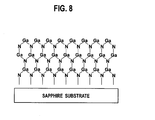
- the GaN semiconductor laminated on the sapphire substrate in the direction (0001) has: a wurtzite crystal structure in the direction (0001) ; and a crystal polarity (which grows in the C axis direction) where the cation elements of Ga are in a growth surface direction as shown in Fig. 7 .
- the layers are laminated in a direction perpendicular to the sapphire substrate, i.e., the C axis [0001] direction.
- Fig. 10 illustrates band gap energies in the valence bands of the lamination region of an n-AlGaN clad layer 41, an n-GaN light guide layer 42, an MQW active layer 43, a p-GaN light guide layer 44 and a p-AlGaN clad layer 45, in a gallium nitride semiconductor emitting element produced by lamination of a GaN semiconductor layer on the above mentioned sapphire substrate.
- Patent Document 1 JP-A 2000-216497
- the Ga polar face is in a growth surface direction in a GaN semiconductor layer laminated on the C face (0001) of a sapphire substrate
- the grown GaN semiconductor layer does not have a symmetry in the C axis direction at its GaN/AlGaN hetero junction interface and has a wurtzite structure, in which the epitaxial membrane grown on the C plane has front and back sides.
- spontaneous polarization and piezo polarization attributable to interface stress occur to thereby generate a polarization charge, and then to generate an electric field at the hetero junction bond interface. This electric field causes electrons to be drawn into the active layer on the n side, creating only a small problem.
- Mg is contained in the p-AlGaN clad layer 45 as a p type impurity.
- this Mg concentration is 1 x 10 19 cm -3 or less, piezo polarization generated at the interface between the p-GaN light guide layer 44 and the p-AlGaN clad layer 45 rapidly increases, causing a problem that an electric field E illustrated in Fig. 10 greatly increases.
- the present invention was made to solve the above described problem, and an object thereof is to provide a gallium nitride semiconductor light emitting element that allows a drive voltage to be stabilized by reducing: carrier depletion due to spontaneous polarization and piezo polarization generated at the interface between an AlGaN semiconductor layer and a GaN semiconductor layer.
- a gallium nitride semiconductor light emitting element which includes at least an n type semiconductor layer, a light emitting region and a p type semiconductor layer, in listed order, on a substrate, and which has an interface between an AlGaN semiconductor layer and a GaN semiconductor layer.
- the AlGaN semiconductor layer is formed at the above p type semiconductor layer side and contains Mg of 10 19 cm -3 or less, and the GaN semiconductor layer is positioned closer to the n layer than the AlGaN semiconductor layer is.
- the gallium nitride semiconductor light emitting element is characterized in that, from the above n type semiconductor layer to the AlGaN semiconductor layer, the growth face is not formed to have nitrogen polarity or Ga polarity of GaN, but is formed in a non-polar direction.
- the invention described in claim 2 is a gallium nitride semiconductor light emitting element which includes at least an n type semiconductor layer, a light emitting region and a p type semiconductor layer, in listed order, on a substrate, and which has an interface between an AlGaN semiconductor layer and an InGaN semiconductor layer.
- the AlGaN semiconductor layer is formed at the above p type semiconductor layer side and contains Mg of 10 19 cm -3 or less, and the InGaN semiconductor layer is positioned on the n side relative to the AlGaN semiconductor layer.
- the gallium nitride semiconductor light emitting element is characterized in that, from the n type semiconductor layer to the AlGaN semiconductor layer, the growth face is not formed to have nitrogen polarity or Ga polarity of GaN, but is formed in a non-polar direction.
- the invention described in claim 3 is a gallium nitride semiconductor light emitting element which includes at least an n type semiconductor layer, a light emitting region and a p type semiconductor layer, in listed order, on a substrate, and which has an interface between an Al x GaN semiconductor layer and an Al Y GaN semiconductor layer (X>Y).
- the Al x GaN semiconductor layer is formed at the above p type semiconductor layer side and contains Mg of 10 19 cm -3 or less, and the Al Y GaN semiconductor layer (X>Y) is positioned on the n side relative to the p type Al x GaN semiconductor layer.
- the gallium nitride semiconductor light emitting element is characterized in that, from the above n type semiconductor layer to the Al x GaN semiconductor layer, the growth face is not formed to have nitrogen polarity or Ga polarity of GaN, but is formed in a non-polar direction.
- the growth direction of a gallium nitride semiconductor laminated on a substrate is formed on a face different from the N (nitrogen) polarity and the Ga polarity of GaN, i.e., the A or M plane.
- N nitrogen
- Ga polarity of GaN i.e., the A or M plane.
- FIG. 1 shows a schematic construction of a gallium nitride semiconductor light emitting element.
- a gallium nitride semiconductor light emitting element of Fig. 1(a) has a gallium nitride semiconductor crystal 2 which contains a light emitting region and is formed on a sapphire substrate 1.
- the gallium nitride semiconductor crystal 2 is formed on the R plane (1-102) of a sapphire substrate 1 by the MOCVD method or the like, and its growth surface grows on the A plane.
- the A plane as shown in Figs. 8 and 9 , is not a Ga polar face or an N (nitrogen) polar face, but a non-polar face.
- JP-A 2000-216497 as Patent Document 1 describes that a GaN semiconductor layer can be laminated using the A plane or the M plane of a sapphire substrate to make the growth face the M plane or the A plane.
- the growth direction becomes the C axis, whereby the growth surface of the GaN semiconductor layer is not considered to be the M plane or the A plane.
- a gallium nitride semiconductor light emitting element of Fig. 1(b) has the gallium nitride semiconductor crystal 2 containing a light emitting region laminated on a GaN substrate 3.
- the gallium nitride semiconductor crystal 2 is formed on the A plane (11-20) of the GaN substrate 3 by the MOCVD method or the like, and its growth surface grows on the A plane.
- the A plane, as described above, is not a Ga polar face or an N (nitrogen) polar face, but a non-polar face.
- a gallium nitride semiconductor light emitting element of Fig. 1(c) has the gallium nitride semiconductor crystal 2 containing a light emitting region laminated on the GaN substrate 3.
- the gallium nitride semiconductor crystal 2 is formed on the M plane (10-10) of the GaN substrate 3 by the MOCVD method or the like, and its growth surface grows on the M plane.
- the M plane as shown in Figs. 8 and 9 , is not a Ga polar face or an N (nitrogen) polar face, but a non-polar face.
- the growth surface of the gallium nitride semiconductor crystal 2 does not become the Ga polar face or the N (nitrogen) polar face, but a non-polar face. Since the strength of an electric field E at the GaN/AlGaN interface of the grown gallium nitride semiconductor crystal 2 becomes very weak as compared with the strength of the electric field E generated when a growth surface is the Ga polar face shown in Fig. 10 , a conventional technique, carrier depletion can be avoided.
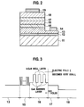
- FIG. 2 One example of an LED in a gallium nitride semiconductor light emitting element is shown in Fig. 2 .
- the gallium nitride semiconductor crystal 2 is grown on the R plane of a sapphire substrate 1 to thereby make the growth surface the A plane.
- a buffer layer 12 On the sapphire substrate 11 are formed a buffer layer 12, an n type contact layer 13, an n type super lattice layer 15, an MQW active layer 16, a p type electron block layer 17 and a p type contact layer 18.
- a positive electrode (p electrode) 20 On the n type contact layer 13 is formed a negative electrode (n electrode) 14.
- the buffer layer 12, the n type contact layer 13, the n type super lattice layer 15, the MQW active layer 16, the p type electron block layer 17 and the p type contact layer 18 all have growth surfaces of the A plane.
- Fig. 3 illustrates band gap energies in valence bands in a case where the buffer layer 12 is constituted by undoped GaN, the n type contact layer 13 is constituted by n-GaN, the n type super lattice layer 15 has a super lattice structure produced by alternately laminating an n-GaN thin film and an n-InGaN thin film for 5 to 10 cycles, the MQW active layer 16 has a multiple quantum well structure constituted by a well layer of InGaN and a barrier layer of GaN or InGaN, respectively, the p type electron block layer 17 is p-AlGaN produced by doping Mg therein as an impurity at a concentration of 1 x 10 19 cm -3 or less, and the p type contact layer 18 is constituted by p-GaN.
- the well-known MOCVD method or the like is used for the growth.
- the buffer layer 12 of approximately 1 to 3 ⁇ m including undoped GaN the Si-doped GaN contact layer 13 of approximately 1 to 5 ⁇ m, and the following layers of approximately 0.2 to 1 ⁇ m, respectively, are laminated sequentially: the Si-doped InGaN/GaN super lattice layer 15; the MQW active layer 16; the Mg-doped AlGaN electron block layer 17; and the Mg-doped GaN contact layer 18.
- the MQW active layer 16 is formed in a multi-layer structure in which a well layer including In 0.17 Ga 0.83 N of 1 to 3 nm and a barrier layer including In X GaN (0 ⁇ X ⁇ 0.05) of 10 to 20 nm are alternately laminated on each other for 3 to 10 cycles.
- parts of the p type contact layer 18, the p type electron block layer 17, the MQW active layer 16, the n type super lattice layer 15 and the n type contact layer 13 are mesa etched by reactive ion etching or the like and removed. Thereafter, on the etched face of the n type contact layer 13 is formed the negative electrode 14 by vapor deposition and on the p type contact layer 18 is formed the positive electrode 19 by vapor deposition.
- FIG. 4 one example of an LD in a gallium nitride semiconductor light emitting element is illustrated in Fig. 4 .
- the gallium nitride semiconductor crystal 2 is grown on the R plane of the sapphire substrate 1 to make the growth surface the A plane.
- the well-known MOCVD method or the like is used for the growth.
- a buffer layer 32 of approximately 1 to 3 ⁇ m including undoped GaN, an n type clad layer 34 of approximately 1 to 5 ⁇ m including an Si-doped AlGaN/GaN super lattice layer, and the following layers of approximately 0.2 to 1 ⁇ m, respectively, are laminated sequentially: an n type super lattice layer 35 including Si-doped InGaN/GaN; an MQW active layer 36; a p type electron block layer 37 including AlGaN produced by doping Mg at a concentration of 1 x 10 19 cm -3 or less; and a p type clad layer 38 including an Mg doped AlGaN/GaN super lattice layer.
- An MQW active layer 36 is formed in a multi-layer structure in which a well layer including In 0.17 Ga 0.83 N of 1 to 3 nm and a barrier layer including In z GaN (0 ⁇ Z ⁇ 0.05) of 10 to 20 nm are alternately laminated on each other for 3 to 10 cycles.
- the ridge side face to the flat part of the p type clad layer 38 are covered with an insulating layer 39 and the ridge part of the p type clad layer 38 is laminated with a p type contact layer 40 including Mg-doped GaN.
- parts of the p type contact layer 40, the p type clad layer 38, the p type electron block layer 37, the MQW active layer 36, the n type super lattice layer 35, the n type clad layer 34 and the buffer layer 32 are mesa etched by reactive ion etching or the like and removed. Thereafter, on the etched face of the buffer layer 32 is formed an n electrode 33 by vapor deposition and on the p type contact layer 40 is formed a p electrode 50 by vapor deposition.
- the buffer layer 32, the n type clad layer 34, the n type super lattice layer 35, the MQW active layer 36, the p type electron block layer 37, the p type clad layer 38 and the p type contact layer 40 all have the A plane as a growth surface.
- an electric field E is generated from the GaN barrier layer toward the p-AlGaN electron block layer 37, as in the case of Fig.
- the strength of the electric field becomes very smaller than the strength of a conventional electric field illustrated in Fig. 10 .
- holes injected from the p electrode 41 side tend to be injected into the MQW active layer 36 side of a light emitting region and, therefore carrier depletion can be avoided.
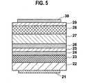
- Fig. 5 shows one example of a gallium nitride semiconductor light emitting element in which the gallium nitride semiconductor crystal 2 is grown on the A plane or M plane of the GaN substrates 3, 4 to make the growth surface the A plane or M plane.
- an LED is formed using the structure of Fig. 5 , by means of the well-known MOCVD method or the like, for example, on the A plane or M plane of a GaN substrate 22, an Si-doped AlGaN of approximately 0.8 ⁇ m as an n type clad layer 23, undoped GaN or n doped GaN of about 0.1 ⁇ m as a n type light guide layer 24, MQW active layer 25, undoped GaN or p doped GaN of about 0.1 ⁇ m as a p type light guide layer 26, AlGaN of 200 ⁇ produced by doping Mg at a concentration of 1 x 10 19 cm -3 or less as an electron block layer 27, a p type clad layer 28 and Mg-doped GaN as a p type contact layer 29 are sequentially laminated.
- an MQW active layer 25 is made to have, for example, a multiple quantum well structure produced by laminating a well layer of In 0.08 GaN of 30 ⁇ and a barrier layer (obstacle layer) of In 0.01 GaN of 150 ⁇ ; the p type clad layer 28 is made to be a super lattice layer produced by alternately laminating undoped AlGaN of 20 ⁇ to 50 ⁇ and Mg-doped GaN of 20 ⁇ to 50 ⁇ .
- a positive electrode 30 (p electrode) and a negative electrode 21 (n electrode) are formed by vapor deposition.
- the n type clad layer 23 undoped GaN or n doped GaN of about 0.1 ⁇ m as the n type light guide layer 24, the MQW active layer 25, undoped GaN or p doped GaN of about 0.1 ⁇ m as the p type light guide layer 26, AlGaN of about 200 ⁇ as the electron block layer 27 produced by doping Mg at a concentration of 1 x 10 19 cm -3 or less, the p type clad layer 28 and Mg-doped GaN as the p type contact layer 29 are sequentially laminated.
- the MQW active layer 25 is made to have, for example, a multiple quantum well structure produced by laminating a well layer including In 0.08 Ga 0.92 N of 30 ⁇ and a barrier layer (obstacle layer) including In 0.01 GaN of 150 ⁇ .
- the n type clad layer 23 is made to be a super lattice layer produced by alternately laminating undoped AlGaN of 20 to 50 ⁇ and Si-doped GaN of 20 to 50 ⁇ .
- the p type clad layer 28 is made to be a super lattice layer produced by alternately laminating undoped AlGaN of 20 to 50 ⁇ and Mg-doped GaN of 20 to 50 ⁇ .
- the positive electrode 30 (p electrode) and the negative electrode 21 (n electrode) are formed by vapor deposition.
- Band gap energies in valence bands when an LED or LD is constituted by the structure of Fig. 5 as described above, are illustrated in Fig. 6 .
- the growth surface becomes a non-polar face, and as shown in Fig. 6 , the strength of the electric field becomes extremely smaller than of a conventional electric field illustrated in Fig. 10 .
- holes injected from the positive electrode 30 side tend to be injected into the MQW active layer 25 side of a light emitting region and, therefore carrier depletion can be avoided.
- an electric field E due to spontaneous polarization and piezo polarization attributable to interface stress is observed not only at the interface of AlGaN/GaN but also at the interface between AlGaN and another GaN semiconductor layer.
- a similar electric field is generated at the interface of AlGaN/InGaN and at the interface of Al X GaN/Al Y GaN (X>Y).
- the barrier layers of the MQW active layers 16, 36 can use InGaN in a structure in Fig. 2 or 4 , and if the structure is utilized, the interface of AlGaN/InGaN is formed between the p type electron block layers 17, 37 of AlGaN and the barrier layer.
- an Al X GaN/Al Y GaN (X > Y) interface may be formed between the p type clad layer 28 of super lattice layers of AlGaN and GaN and the electron block layer 27 of AlGaN.
- Fig. 7 (a) illustrates a state of the interface of AlGaN/InGaN
- Fig. 7(b) illustrates a state of the interface of Al X GaN/Al Y GaN (X > Y) together with band energies in valance electron bands.
- a gallium nitride semiconductor crystal When the growth surface of a gallium nitride semiconductor crystal is a Ga polar face, holes from the p electrode side receive electric repulsion to thereby be less likely injected into the light emitting region even at each interface described above.
- the growth direction of the semiconductor layer of a gallium nitride semiconductor crystal is made to be from a non-polar face, as illustrated in Fig. 7 (a) , the strength of an electric field E generated from the InGaN semiconductor layer toward the AlGaN semiconductor layer at the interface of AlGaN/InGaN can be made very small.
- holes can be easily injected from the p electrode side into the light emitting region.
- the doping concentration of the impurity Mg in the AlGaN semiconductor layer or the aforementioned Al Y GaN semiconductor layer becomes 1 x 10 19 cm -3 or less
- the growth face is the Ga polar face
- an electric field of a very large strength is generated at each interface of AlGaN/InGaN, AlGaN/GaN and Al X GaN/Al Y GaN (X > Y).
- the growth surface is made to be a non-polar face, the strength of an electric field at each interface above can be extremely decreased. Thus, holes from the p electrode side can be readily injected into the light emitting region.
Landscapes
- Physics & Mathematics (AREA)
- Optics & Photonics (AREA)
- Engineering & Computer Science (AREA)
- Condensed Matter Physics & Semiconductors (AREA)
- General Physics & Mathematics (AREA)
- Electromagnetism (AREA)
- Nanotechnology (AREA)
- Chemical & Material Sciences (AREA)
- Biophysics (AREA)
- Crystallography & Structural Chemistry (AREA)
- Life Sciences & Earth Sciences (AREA)
- Led Devices (AREA)
- Semiconductor Lasers (AREA)
Applications Claiming Priority (2)
| Application Number | Priority Date | Filing Date | Title |
|---|---|---|---|
| JP2005346845A JP5113330B2 (ja) | 2005-11-30 | 2005-11-30 | 窒化ガリウム半導体発光素子 |
| PCT/JP2006/323853 WO2007063920A1 (ja) | 2005-11-30 | 2006-11-29 | 窒化ガリウム半導体発光素子 |
Publications (1)
| Publication Number | Publication Date |
|---|---|
| EP1959530A1 true EP1959530A1 (de) | 2008-08-20 |
Family
ID=38092254
Family Applications (1)
| Application Number | Title | Priority Date | Filing Date |
|---|---|---|---|
| EP06833656A Withdrawn EP1959530A1 (de) | 2005-11-30 | 2006-11-29 | Galliumnitrid-halbleiterleuchtbauelement |
Country Status (7)
| Country | Link |
|---|---|
| US (1) | US7872269B2 (de) |
| EP (1) | EP1959530A1 (de) |
| JP (1) | JP5113330B2 (de) |
| KR (1) | KR20080075212A (de) |
| CN (1) | CN101322292B (de) |
| TW (1) | TW200737632A (de) |
| WO (1) | WO2007063920A1 (de) |
Cited By (9)
| Publication number | Priority date | Publication date | Assignee | Title |
|---|---|---|---|---|
| WO2009141724A1 (en) * | 2008-05-23 | 2009-11-26 | S.O.I.Tec Silicon On Insulator Technologies | Formation of substantially pit free indium gallium nitride |
| EP2565940A3 (de) * | 2011-08-31 | 2015-02-11 | LG Innotek Co., Ltd. | Lichtemittierende Vorrichtung |
| EP4231365A1 (de) * | 2022-02-18 | 2023-08-23 | Epinovatech AB | Lichtemittierende vorrichtung und verfahren zur herstellung einer lichtemittierenden vorrichtung |
| US12355442B2 (en) | 2020-03-13 | 2025-07-08 | Epinovatech Ab | Field-programmable gate array device |
| US12382656B2 (en) | 2018-04-22 | 2025-08-05 | Epinovatech Ab | Reinforced thin-film device |
| US12395027B2 (en) | 2020-05-07 | 2025-08-19 | Epinovatech Ab | Induction machine |
| US12456734B2 (en) | 2020-01-24 | 2025-10-28 | Epinovatech Ab | Solid-state battery layer structure and method for producing the same |
| US12557325B2 (en) | 2020-05-29 | 2026-02-17 | Epinovatech Ab | Vertical HEMT and a method to produce a vertical HEMT |
| US12563670B2 (en) | 2021-05-10 | 2026-02-24 | Epinovatech Ab | Power converter device and a system comprising the same |
Families Citing this family (35)
| Publication number | Priority date | Publication date | Assignee | Title |
|---|---|---|---|---|
| US8809867B2 (en) | 2002-04-15 | 2014-08-19 | The Regents Of The University Of California | Dislocation reduction in non-polar III-nitride thin films |
| WO2003089695A1 (en) * | 2002-04-15 | 2003-10-30 | The Regents Of The University Of California | Non-polar a-plane gallium nitride thin films grown by metalorganic chemical vapor deposition |
| KR100920915B1 (ko) | 2006-12-28 | 2009-10-12 | 서울옵토디바이스주식회사 | 초격자 구조의 장벽층을 갖는 발광 다이오드 |
| EP1976031A3 (de) | 2007-03-29 | 2010-09-08 | Seoul Opto Device Co., Ltd. | Lichtemittierende Diode mit Bohr- und/oder Sperrschichten mit Übergitterstruktur |
| JP2009004538A (ja) * | 2007-06-21 | 2009-01-08 | Panasonic Corp | 半導体レーザ装置 |
| JP2009021361A (ja) | 2007-07-11 | 2009-01-29 | Sumitomo Electric Ind Ltd | 窒化物系半導体発光素子、および窒化物系半導体発光素子を作製する方法 |
| JP5041902B2 (ja) * | 2007-07-24 | 2012-10-03 | 三洋電機株式会社 | 半導体レーザ素子 |
| JP4605193B2 (ja) | 2007-07-27 | 2011-01-05 | 豊田合成株式会社 | Iii族窒化物系化合物半導体素子 |
| CN101364628B (zh) * | 2007-08-06 | 2013-06-26 | 晶元光电股份有限公司 | 半导体发光装置及其制造方法 |
| JP5022136B2 (ja) | 2007-08-06 | 2012-09-12 | 三洋電機株式会社 | 半導体素子の製造方法および半導体素子 |
| US20090050874A1 (en) | 2007-08-20 | 2009-02-26 | Samsung Electro-Mechanics Co., Ltd. | Nitride semiconductor light emitting device |
| KR100877774B1 (ko) * | 2007-09-10 | 2009-01-16 | 서울옵토디바이스주식회사 | 개선된 구조의 발광다이오드 |
| KR100889956B1 (ko) * | 2007-09-27 | 2009-03-20 | 서울옵토디바이스주식회사 | 교류용 발광다이오드 |
| US8144743B2 (en) | 2008-03-05 | 2012-03-27 | Rohm Co., Ltd. | Nitride based semiconductor device and fabrication method for the same |
| JP5164641B2 (ja) * | 2008-04-02 | 2013-03-21 | Dowaエレクトロニクス株式会社 | 電流狭窄型半導体発光素子の製造方法 |
| JP2011517099A (ja) * | 2008-04-04 | 2011-05-26 | ザ リージェンツ オブ ザ ユニバーシティ オブ カリフォルニア | プレーナー半極性(Al,In,Ga,B)Nベースの発光ダイオード向けMOCVD成長技術 |
| KR100957750B1 (ko) | 2008-08-12 | 2010-05-13 | 우리엘에스티 주식회사 | 발광 소자 |
| KR101507130B1 (ko) | 2008-11-20 | 2015-03-30 | 서울바이오시스 주식회사 | 초격자층을 갖는 발광 다이오드 |
| US20100123119A1 (en) * | 2008-11-20 | 2010-05-20 | Seoul Opto Device Co., Ltd. | Light emitting diode having indium nitride |
| JP2010272593A (ja) * | 2009-05-19 | 2010-12-02 | Hamamatsu Photonics Kk | 窒化物半導体発光素子及びその製造方法 |
| JP5434573B2 (ja) * | 2009-12-24 | 2014-03-05 | 豊田合成株式会社 | Iii族窒化物系化合物半導体素子 |
| JP4929367B2 (ja) * | 2010-03-08 | 2012-05-09 | 株式会社東芝 | 半導体発光素子及びその製造方法 |
| US9178108B2 (en) * | 2010-05-24 | 2015-11-03 | Lg Innotek Co., Ltd. | Light emitting device and light emitting device package |
| JP2012064728A (ja) | 2010-09-15 | 2012-03-29 | Stanley Electric Co Ltd | 光源装置 |
| JP5744615B2 (ja) * | 2011-04-28 | 2015-07-08 | シャープ株式会社 | 窒化物半導体発光ダイオード素子 |
| US8907319B2 (en) * | 2011-12-12 | 2014-12-09 | Lg Innotek Co., Ltd. | Light emitting device package |
| JP5734250B2 (ja) * | 2012-08-30 | 2015-06-17 | Dowaエレクトロニクス株式会社 | 電流狭窄型半導体発光素子 |
| JP2015119171A (ja) * | 2013-11-13 | 2015-06-25 | スタンレー電気株式会社 | 多重量子井戸半導体発光素子 |
| CN104835893B (zh) * | 2015-05-29 | 2017-06-13 | 东南大学 | 基于金属氮化物半导体的氮极性面发光二极管及制备方法 |
| JP2017143139A (ja) * | 2016-02-09 | 2017-08-17 | 株式会社東芝 | 半導体装置およびその製造方法 |
| CN107819058B (zh) * | 2017-11-28 | 2019-07-23 | 厦门三安光电有限公司 | 发光二极管 |
| JP7244745B2 (ja) | 2019-02-15 | 2023-03-23 | 日亜化学工業株式会社 | 発光装置、及び、光学装置 |
| CN111599903B (zh) * | 2020-06-23 | 2022-03-08 | 东南大学 | 一种具有极化掺杂复合极性面电子阻挡层的紫外led |
| KR102689679B1 (ko) * | 2022-11-09 | 2024-07-30 | 웨이브로드 주식회사 | 그룹3족 질화물 반도체 템플릿의 제조 방법 |
| CN116504888B (zh) * | 2023-04-27 | 2024-07-05 | 江苏第三代半导体研究院有限公司 | 一种外延片及其制备方法和应用 |
Family Cites Families (9)
| Publication number | Priority date | Publication date | Assignee | Title |
|---|---|---|---|---|
| EP0772249B1 (de) * | 1995-11-06 | 2006-05-03 | Nichia Corporation | Halbleitervorrichtung aus einer Nitridverbindung |
| JP2000216497A (ja) | 1999-01-22 | 2000-08-04 | Sanyo Electric Co Ltd | 半導体素子およびその製造方法 |
| JP3646872B2 (ja) * | 2000-07-31 | 2005-05-11 | 日本電信電話株式会社 | 窒化物半導体成長方法および窒化物半導体発光素子 |
| JP2002076519A (ja) * | 2000-08-30 | 2002-03-15 | Fujitsu Ltd | 半導体レーザ |
| JP2002164623A (ja) * | 2000-11-24 | 2002-06-07 | Nippon Telegr & Teleph Corp <Ntt> | 窒化物半導体レーザ及びその製造方法 |
| US7186302B2 (en) * | 2002-12-16 | 2007-03-06 | The Regents Of The University Of California | Fabrication of nonpolar indium gallium nitride thin films, heterostructures and devices by metalorganic chemical vapor deposition |
| JP2004335559A (ja) * | 2003-04-30 | 2004-11-25 | Nichia Chem Ind Ltd | Iii族窒化物基板を用いる半導体素子 |
| JP4140606B2 (ja) * | 2005-01-11 | 2008-08-27 | ソニー株式会社 | GaN系半導体発光素子の製造方法 |
| KR100835116B1 (ko) * | 2007-04-16 | 2008-06-05 | 삼성전기주식회사 | 질화물 반도체 발광 소자 |
-
2005
- 2005-11-30 JP JP2005346845A patent/JP5113330B2/ja not_active Expired - Fee Related
-
2006
- 2006-11-29 WO PCT/JP2006/323853 patent/WO2007063920A1/ja not_active Ceased
- 2006-11-29 KR KR1020087015914A patent/KR20080075212A/ko not_active Withdrawn
- 2006-11-29 EP EP06833656A patent/EP1959530A1/de not_active Withdrawn
- 2006-11-29 US US12/085,836 patent/US7872269B2/en not_active Expired - Fee Related
- 2006-11-29 CN CN2006800451527A patent/CN101322292B/zh not_active Expired - Fee Related
- 2006-11-30 TW TW095144430A patent/TW200737632A/zh unknown
Non-Patent Citations (1)
| Title |
|---|
| See references of WO2007063920A1 * |
Cited By (11)
| Publication number | Priority date | Publication date | Assignee | Title |
|---|---|---|---|---|
| WO2009141724A1 (en) * | 2008-05-23 | 2009-11-26 | S.O.I.Tec Silicon On Insulator Technologies | Formation of substantially pit free indium gallium nitride |
| EP2565940A3 (de) * | 2011-08-31 | 2015-02-11 | LG Innotek Co., Ltd. | Lichtemittierende Vorrichtung |
| US12382656B2 (en) | 2018-04-22 | 2025-08-05 | Epinovatech Ab | Reinforced thin-film device |
| US12456734B2 (en) | 2020-01-24 | 2025-10-28 | Epinovatech Ab | Solid-state battery layer structure and method for producing the same |
| US12355442B2 (en) | 2020-03-13 | 2025-07-08 | Epinovatech Ab | Field-programmable gate array device |
| US12395027B2 (en) | 2020-05-07 | 2025-08-19 | Epinovatech Ab | Induction machine |
| US12557325B2 (en) | 2020-05-29 | 2026-02-17 | Epinovatech Ab | Vertical HEMT and a method to produce a vertical HEMT |
| US12563670B2 (en) | 2021-05-10 | 2026-02-24 | Epinovatech Ab | Power converter device and a system comprising the same |
| EP4231365A1 (de) * | 2022-02-18 | 2023-08-23 | Epinovatech AB | Lichtemittierende vorrichtung und verfahren zur herstellung einer lichtemittierenden vorrichtung |
| WO2023156428A1 (en) * | 2022-02-18 | 2023-08-24 | Epinovatech Ab | A device for emitting light and a method for producing a light-emitting device |
| EP4480013A1 (de) * | 2022-02-18 | 2024-12-25 | Epinovatech AB | Vorrichtung zur lichtemission und verfahren zur herstellung einer lichtemittierenden vorrichtung |
Also Published As
| Publication number | Publication date |
|---|---|
| KR20080075212A (ko) | 2008-08-14 |
| WO2007063920A1 (ja) | 2007-06-07 |
| US7872269B2 (en) | 2011-01-18 |
| TW200737632A (en) | 2007-10-01 |
| CN101322292B (zh) | 2012-04-18 |
| CN101322292A (zh) | 2008-12-10 |
| JP5113330B2 (ja) | 2013-01-09 |
| US20090146160A1 (en) | 2009-06-11 |
| JP2007157766A (ja) | 2007-06-21 |
Similar Documents
| Publication | Publication Date | Title |
|---|---|---|
| US7872269B2 (en) | Gallium nitride semiconductor light emitting element | |
| US8017932B2 (en) | Light-emitting device | |
| US6803596B2 (en) | Light emitting device | |
| JP4924185B2 (ja) | 窒化物半導体発光素子 | |
| US7974322B2 (en) | Nitride semiconductor laser diode | |
| JP3705047B2 (ja) | 窒化物半導体発光素子 | |
| US20030179793A1 (en) | Thin film deposition method of nitride semiconductor and nitride semiconductor light emitting device | |
| KR20030064629A (ko) | 반도체 발광 소자 및 그 제조 방법 | |
| KR20040018348A (ko) | 질화 갈륨계 화합물 반도체 소자 | |
| KR20060114683A (ko) | GaN계 Ⅲ-V족 화합물 반도체 발광 소자 및 그 제조방법 | |
| US8803274B2 (en) | Nitride-based semiconductor light-emitting element | |
| JP2008288527A (ja) | レーザ発光装置 | |
| JPWO2009057254A1 (ja) | 半導体レーザ装置 | |
| US20070008998A1 (en) | Semiconductor light emitting device | |
| JPH08316581A (ja) | 半導体装置および半導体発光素子 | |
| US7755101B2 (en) | Semiconductor light emitting device | |
| JPH11191639A (ja) | 窒化物半導体素子 | |
| JP4877294B2 (ja) | 半導体発光素子の製造方法 | |
| JP2003086903A (ja) | 半導体発光素子およびその製造方法 | |
| JP4212105B2 (ja) | 酸化亜鉛系化合物半導体素子 | |
| JP3711020B2 (ja) | 発光素子 | |
| JP4178807B2 (ja) | 半導体発光素子およびその製造方法 | |
| JP2004104088A (ja) | 窒化物半導体素子 | |
| JP3464890B2 (ja) | 半導体発光装置 | |
| JP2002261370A (ja) | 窒化物系半導体素子の作製方法 |
Legal Events
| Date | Code | Title | Description |
|---|---|---|---|
| PUAI | Public reference made under article 153(3) epc to a published international application that has entered the european phase |
Free format text: ORIGINAL CODE: 0009012 |
|
| 17P | Request for examination filed |
Effective date: 20080611 |
|
| AK | Designated contracting states |
Kind code of ref document: A1 Designated state(s): DE FR GB |
|
| DAX | Request for extension of the european patent (deleted) | ||
| RBV | Designated contracting states (corrected) |
Designated state(s): DE FR GB |
|
| STAA | Information on the status of an ep patent application or granted ep patent |
Free format text: STATUS: THE APPLICATION HAS BEEN WITHDRAWN |
|
| 18W | Application withdrawn |
Effective date: 20101209 |