EP1960194B1 - Verfahren zur herstellung eines leitenden musters und durch das verfahren hergestelltes leitendes muster - Google Patents
Verfahren zur herstellung eines leitenden musters und durch das verfahren hergestelltes leitendes muster Download PDFInfo
- Publication number
- EP1960194B1 EP1960194B1 EP06835222.8A EP06835222A EP1960194B1 EP 1960194 B1 EP1960194 B1 EP 1960194B1 EP 06835222 A EP06835222 A EP 06835222A EP 1960194 B1 EP1960194 B1 EP 1960194B1
- Authority
- EP
- European Patent Office
- Prior art keywords
- conductive pattern
- solution containing
- ions
- reducing metal
- metal ions
- Prior art date
- Legal status (The legal status is an assumption and is not a legal conclusion. Google has not performed a legal analysis and makes no representation as to the accuracy of the status listed.)
- Not-in-force
Links
Images
Classifications
-
- G—PHYSICS
- G02—OPTICS
- G02B—OPTICAL ELEMENTS, SYSTEMS OR APPARATUS
- G02B5/00—Optical elements other than lenses
- G02B5/20—Filters
- G02B5/204—Filters in which spectral selection is performed by means of a conductive grid or array, e.g. frequency selective surfaces
-
- B—PERFORMING OPERATIONS; TRANSPORTING
- B32—LAYERED PRODUCTS
- B32B—LAYERED PRODUCTS, i.e. PRODUCTS BUILT-UP OF STRATA OF FLAT OR NON-FLAT, e.g. CELLULAR OR HONEYCOMB, FORM
- B32B27/00—Layered products comprising a layer of synthetic resin
- B32B27/06—Layered products comprising a layer of synthetic resin as the main or only constituent of a layer, which is next to another layer of the same or of a different material
-
- B—PERFORMING OPERATIONS; TRANSPORTING
- B32—LAYERED PRODUCTS
- B32B—LAYERED PRODUCTS, i.e. PRODUCTS BUILT-UP OF STRATA OF FLAT OR NON-FLAT, e.g. CELLULAR OR HONEYCOMB, FORM
- B32B15/00—Layered products comprising a layer of metal
- B32B15/04—Layered products comprising a layer of metal comprising metal as the main or only constituent of a layer, which is next to another layer of the same or of a different material
- B32B15/08—Layered products comprising a layer of metal comprising metal as the main or only constituent of a layer, which is next to another layer of the same or of a different material of synthetic resin
-
- B—PERFORMING OPERATIONS; TRANSPORTING
- B32—LAYERED PRODUCTS
- B32B—LAYERED PRODUCTS, i.e. PRODUCTS BUILT-UP OF STRATA OF FLAT OR NON-FLAT, e.g. CELLULAR OR HONEYCOMB, FORM
- B32B3/00—Layered products comprising a layer with external or internal discontinuities or unevennesses, or a layer of non-planar shape; Layered products comprising a layer having particular features of form
- B32B3/26—Layered products comprising a layer with external or internal discontinuities or unevennesses, or a layer of non-planar shape; Layered products comprising a layer having particular features of form characterised by a particular shape of the outline of the cross-section of a continuous layer; characterised by a layer with cavities or internal voids ; characterised by an apertured layer
-
- B—PERFORMING OPERATIONS; TRANSPORTING
- B32—LAYERED PRODUCTS
- B32B—LAYERED PRODUCTS, i.e. PRODUCTS BUILT-UP OF STRATA OF FLAT OR NON-FLAT, e.g. CELLULAR OR HONEYCOMB, FORM
- B32B38/00—Ancillary operations in connection with laminating processes
- B32B38/08—Impregnating
-
- C—CHEMISTRY; METALLURGY
- C23—COATING METALLIC MATERIAL; COATING MATERIAL WITH METALLIC MATERIAL; CHEMICAL SURFACE TREATMENT; DIFFUSION TREATMENT OF METALLIC MATERIAL; COATING BY VACUUM EVAPORATION, BY SPUTTERING, BY ION IMPLANTATION OR BY CHEMICAL VAPOUR DEPOSITION, IN GENERAL; INHIBITING CORROSION OF METALLIC MATERIAL OR INCRUSTATION IN GENERAL
- C23C—COATING METALLIC MATERIAL; COATING MATERIAL WITH METALLIC MATERIAL; SURFACE TREATMENT OF METALLIC MATERIAL BY DIFFUSION INTO THE SURFACE, BY CHEMICAL CONVERSION OR SUBSTITUTION; COATING BY VACUUM EVAPORATION, BY SPUTTERING, BY ION IMPLANTATION OR BY CHEMICAL VAPOUR DEPOSITION, IN GENERAL
- C23C22/00—Chemical surface treatment of metallic material by reaction of the surface with a reactive liquid, leaving reaction products of surface material in the coating, e.g. conversion coatings, passivation of metals
- C23C22/05—Chemical surface treatment of metallic material by reaction of the surface with a reactive liquid, leaving reaction products of surface material in the coating, e.g. conversion coatings, passivation of metals using aqueous solutions
- C23C22/06—Chemical surface treatment of metallic material by reaction of the surface with a reactive liquid, leaving reaction products of surface material in the coating, e.g. conversion coatings, passivation of metals using aqueous solutions using aqueous acidic solutions with pH less than 6
- C23C22/48—Chemical surface treatment of metallic material by reaction of the surface with a reactive liquid, leaving reaction products of surface material in the coating, e.g. conversion coatings, passivation of metals using aqueous solutions using aqueous acidic solutions with pH less than 6 not containing phosphates, hexavalent chromium compounds, fluorides or complex fluorides, molybdates, tungstates, vanadates or oxalates
- C23C22/58—Treatment of other metallic material
-
- C—CHEMISTRY; METALLURGY
- C23—COATING METALLIC MATERIAL; COATING MATERIAL WITH METALLIC MATERIAL; CHEMICAL SURFACE TREATMENT; DIFFUSION TREATMENT OF METALLIC MATERIAL; COATING BY VACUUM EVAPORATION, BY SPUTTERING, BY ION IMPLANTATION OR BY CHEMICAL VAPOUR DEPOSITION, IN GENERAL; INHIBITING CORROSION OF METALLIC MATERIAL OR INCRUSTATION IN GENERAL
- C23C—COATING METALLIC MATERIAL; COATING MATERIAL WITH METALLIC MATERIAL; SURFACE TREATMENT OF METALLIC MATERIAL BY DIFFUSION INTO THE SURFACE, BY CHEMICAL CONVERSION OR SUBSTITUTION; COATING BY VACUUM EVAPORATION, BY SPUTTERING, BY ION IMPLANTATION OR BY CHEMICAL VAPOUR DEPOSITION, IN GENERAL
- C23C22/00—Chemical surface treatment of metallic material by reaction of the surface with a reactive liquid, leaving reaction products of surface material in the coating, e.g. conversion coatings, passivation of metals
- C23C22/05—Chemical surface treatment of metallic material by reaction of the surface with a reactive liquid, leaving reaction products of surface material in the coating, e.g. conversion coatings, passivation of metals using aqueous solutions
- C23C22/68—Chemical surface treatment of metallic material by reaction of the surface with a reactive liquid, leaving reaction products of surface material in the coating, e.g. conversion coatings, passivation of metals using aqueous solutions using aqueous solutions with pH between 6 and 8
-
- H—ELECTRICITY
- H05—ELECTRIC TECHNIQUES NOT OTHERWISE PROVIDED FOR
- H05K—PRINTED CIRCUITS; CASINGS OR CONSTRUCTIONAL DETAILS OF ELECTRIC APPARATUS; MANUFACTURE OF ASSEMBLAGES OF ELECTRICAL COMPONENTS
- H05K9/00—Screening of apparatus or components against electric or magnetic fields
- H05K9/0073—Shielding materials
- H05K9/0094—Shielding materials being light-transmitting, e.g. transparent, translucent
- H05K9/0096—Shielding materials being light-transmitting, e.g. transparent, translucent for television displays, e.g. plasma display panel
-
- G—PHYSICS
- G02—OPTICS
- G02B—OPTICAL ELEMENTS, SYSTEMS OR APPARATUS
- G02B1/00—Optical elements characterised by the material of which they are made; Optical coatings for optical elements
- G02B1/10—Optical coatings produced by application to, or surface treatment of, optical elements
- G02B1/11—Anti-reflection coatings
-
- G—PHYSICS
- G02—OPTICS
- G02B—OPTICAL ELEMENTS, SYSTEMS OR APPARATUS
- G02B5/00—Optical elements other than lenses
- G02B5/20—Filters
- G02B5/208—Filters for use with infrared or ultraviolet radiation, e.g. for separating visible light from infrared and/or ultraviolet radiation
-
- G—PHYSICS
- G02—OPTICS
- G02B—OPTICAL ELEMENTS, SYSTEMS OR APPARATUS
- G02B5/00—Optical elements other than lenses
- G02B5/20—Filters
- G02B5/22—Absorbing filters
- G02B5/223—Absorbing filters containing organic substances, e.g. dyes, inks or pigments
-
- H—ELECTRICITY
- H05—ELECTRIC TECHNIQUES NOT OTHERWISE PROVIDED FOR
- H05K—PRINTED CIRCUITS; CASINGS OR CONSTRUCTIONAL DETAILS OF ELECTRIC APPARATUS; MANUFACTURE OF ASSEMBLAGES OF ELECTRICAL COMPONENTS
- H05K1/00—Printed circuits
- H05K1/02—Details
-
- H—ELECTRICITY
- H05—ELECTRIC TECHNIQUES NOT OTHERWISE PROVIDED FOR
- H05K—PRINTED CIRCUITS; CASINGS OR CONSTRUCTIONAL DETAILS OF ELECTRIC APPARATUS; MANUFACTURE OF ASSEMBLAGES OF ELECTRICAL COMPONENTS
- H05K2201/00—Indexing scheme relating to printed circuits covered by H05K1/00
- H05K2201/01—Dielectrics
- H05K2201/0104—Properties and characteristics in general
- H05K2201/0112—Absorbing light, e.g. dielectric layer with carbon filler for laser processing
-
- H—ELECTRICITY
- H05—ELECTRIC TECHNIQUES NOT OTHERWISE PROVIDED FOR
- H05K—PRINTED CIRCUITS; CASINGS OR CONSTRUCTIONAL DETAILS OF ELECTRIC APPARATUS; MANUFACTURE OF ASSEMBLAGES OF ELECTRICAL COMPONENTS
- H05K2203/00—Indexing scheme relating to apparatus or processes for manufacturing printed circuits covered by H05K3/00
- H05K2203/03—Metal processing
- H05K2203/0315—Oxidising metal
-
- Y—GENERAL TAGGING OF NEW TECHNOLOGICAL DEVELOPMENTS; GENERAL TAGGING OF CROSS-SECTIONAL TECHNOLOGIES SPANNING OVER SEVERAL SECTIONS OF THE IPC; TECHNICAL SUBJECTS COVERED BY FORMER USPC CROSS-REFERENCE ART COLLECTIONS [XRACs] AND DIGESTS
- Y10—TECHNICAL SUBJECTS COVERED BY FORMER USPC
- Y10T—TECHNICAL SUBJECTS COVERED BY FORMER US CLASSIFICATION
- Y10T428/00—Stock material or miscellaneous articles
- Y10T428/24—Structurally defined web or sheet [e.g., overall dimension, etc.]
- Y10T428/24802—Discontinuous or differential coating, impregnation or bond [e.g., artwork, printing, retouched photograph, etc.]
-
- Y—GENERAL TAGGING OF NEW TECHNOLOGICAL DEVELOPMENTS; GENERAL TAGGING OF CROSS-SECTIONAL TECHNOLOGIES SPANNING OVER SEVERAL SECTIONS OF THE IPC; TECHNICAL SUBJECTS COVERED BY FORMER USPC CROSS-REFERENCE ART COLLECTIONS [XRACs] AND DIGESTS
- Y10—TECHNICAL SUBJECTS COVERED BY FORMER USPC
- Y10T—TECHNICAL SUBJECTS COVERED BY FORMER US CLASSIFICATION
- Y10T428/00—Stock material or miscellaneous articles
- Y10T428/24—Structurally defined web or sheet [e.g., overall dimension, etc.]
- Y10T428/24802—Discontinuous or differential coating, impregnation or bond [e.g., artwork, printing, retouched photograph, etc.]
- Y10T428/24917—Discontinuous or differential coating, impregnation or bond [e.g., artwork, printing, retouched photograph, etc.] including metal layer
Definitions
- the present invention relates to a method for preparing a conductive pattern, which sufficiently blackens the conductive pattern, reduces the sheet resistance, and allows easy blackening processing of the conductive pattern, thereby improving the productivity and reducing the production cost, and to a conductive pattern prepared therefrom.
- the term “display device” comprehensively refers to monitors for TV, computers, or the like, and includes a display assembly containing a display panel for forming image, and a casing for supporting the display assembly.
- the display assembly includes a display panel such as CRT (Cathode Ray Tube), LCD (Liquid Crystal Display) and PDP (Plasma display Panel) for forming image, a circuit board for driving the display panel and an optical filter disposed in front of the display panel.
- a display panel such as CRT (Cathode Ray Tube), LCD (Liquid Crystal Display) and PDP (Plasma display Panel) for forming image
- a circuit board for driving the display panel and an optical filter disposed in front of the display panel.
- the optical filter comprises an anti-reflection film for preventing the external light incident from the outside from be reflected outward again, a near infrared ray shielding film for shielding the near infrared ray generated in the display panel for prevention of misoperation of an electronic instrument such as a remote controller, a color correction film for enhancing the color purity through control of the shade by incorporation of a color adjusting dye, and an EMI(electromagnetic interference) shielding film for shielding the EMI(electromagnetic interference) generated in the display panel upon driving the display device.
- the EMI(electromagnetic interference) shielding film comprises a substrate made from transparent materials, and a conductive pattern made from metallic materials patterned by a photolithography process, having excellent electric conductivity such as silver and copper.
- the conductive pattern is provided with high-gloss metal materials, light incident from the outside is reflected, or the image light from the display panel is reflected, which may cause reduction of the contrast ratio.
- the surface of the conductive pattern is generally subject to blackening processing. That is, the conductive pattern is usually blackened.
- KR Patent Application Publication No. 2004-0072993 discloses a process for blackening processing of a mesh using chemicals such as concentrated nitric acid after forming the mesh on a metal foil by photolithography.
- Japanese Patent Application Publication No. 2001-210988 discloses a process for blackening processing of the surface of a mesh formed by photolithography, using concentrated nitric acid.
- the conductive pattern is blackened, there are provided problems that the processing time is too long, and that sufficient degree of blackness cannot be obtained. Further, there is also a problem that the sheet resistance of the conductive pattern affecting the ability of shielding the EMI(electromagnetic interference) is increased.
- JP2000013088 discloses an electromagnetic shielding film manufacturing method that involves forming a pattern with a silver paste and electroplating the pattern with copper, thereby enhancing electromagnetic wave shielding performance, transparency and non-visibility.
- one embodiment of the present invention provides a method according to claim 1 for preparing a conductive pattern, comprising a pattern forming step of forming a conductive pattern on a substrate; and a blackening processing step of blackening the surface of the conductive pattern by immersing the conductive pattern in an aqueous solution containing reducing metal ions to oxidize the surface of the conductive pattern.
- Another embodiment of the present invention provides a conductive pattern according to claim 5.
- Still another embodiment of the present invention provides an EMI(electromagnetic interference) shielding film comprising the above-described conductive pattern.
- Still another embodiment of the present invention provides an optical filter for a display device comprising the above-described EMI(electromagnetic interference) shielding film.
- the method for preparing the conductive pattern comprises a pattern forming step of forming a conductive pattern on a substrate; and a blackening processing step of blackening the surface of the conductive pattern by immersing the conductive pattern in an aqueous solution containing reducing metal ions to oxidize the surface of the conductive pattern.
- the substrate can be formed of at least one resin selected from a polyacrylic resin, a polyurethane resin, a polyester resin, a polyepoxy resin, a polyolefin resin, a polycarbonate resin and a cellulose resin.
- the conductive pattern is a silver(Ag) conductive pattern comprising silver(Ag) powders.
- the silver(Ag) conductive pattern is formed by directly printing a conductive paste containing silver(Ag) powders on the substrate.
- a conductive paste containing silver(Ag) powders for this, any method selected from an off-set printing method, a screen printing method, a gravure printing method and an ink-jet printing method can be used.
- any printing method well-known to a skilled person in the art, in which a conductive paste can be directly printed on a substrate can be employed.
- the off-set printing method can comprise the steps of: filling the conductive paste in the concave part formed on a concave plate; contacting a printing blanket with the concave plate to transfer the conductive paste from the concave part of the concave plate to the printing blanket; and contacting the printing blanket with the substrate, and transferring the conductive paste from the printing blanket to the substrate to form a conductive pattern on the substrate.
- a convex plate can be used instead of the concave plate.
- reducing metal ion means a metal ion which exhibits a phenomenon that oxidation number was decreased by receiving electrons from the conductive pattern in contact with the conductive pattern in the present invention.
- the aqueous solution containing the reducing metal ions may be an aqueous solution containing Fe or Cu ions as the reducing metal ions.
- the reducing metal ions are not limited to Fe and Cu, but a variety of reducing metal ions which can satisfy the condition of oxidizing the surface of the conductive pattern can be variously employed.
- the blackening processing step by immersing the conductive pattern in an aqueous solution containing the reducing metal ions, the surface of the conductive pattern is oxidized by reduction of the reducing metal ions, whereby the conductive pattern can be sufficiently blackened.
- the aqueous solution containing the reducing metal ions further comprises Cl ions, in addition to the reducing metal ions.
- the silver(Ag) conductive pattern is immersed in the aqueous solution containing the Cl ions and the reducing metal ions to cause a crystal growth phenomenon by the Cl ions. Accordingly, chlorine salt (Cl salt) crystals are formed on the surface of the conductive pattern.
- the chlorine salt (Cl salt) crystals are formed on the surface of the conductive pattern, the sheet resistance ( ⁇ / ⁇ ) of the conductive pattern is reduced, and correspondingly the conductance is enhanced.
- the aqueous solution containing the reducing metal ions can be selected from anaqueous FeCl 3 solution, an aqueous CuCl 2 solution and an aqueous K 3 Fe(CN) 6 solution added with a solution containing Cl ions.
- an aqueous FeCl 2 solution can be used as the aqueous solution containing the reducing metal ions.
- the aqueous FeCl 3 solution may comprise 0.01 to 50% by weight of FeCl 3 and balance q. s. to 100% by weight of water, based on the total weight.
- the aqueous CuCl 2 solution may comprise 0.01 to 50% by weight of CuCl 2 and balance q. s. to 100% by weight of water, based on the total weight.
- the aqueous K 3 Fe(CN) 6 solution may comprise 0.01 to 50% by weight of K 3 Fe(CN) 6 , 0.01 to 50% by weight of the solution containing Cl ions, and balance q. s. to 100% by weight of water, based on the total weight.
- the solution containing Cl ions added to the aqueous K 3 Fe(CN) 6 solution is preferably HCl, but is not limited thereto.
- the conductive pattern is a silver (Ag) conductive pattern obtained by directly printing a conductive paste comprising silver(Ag) powders on the substrate, and if the aqueous solution containing the reducing metal ions further comprises Cl ions, if the silver (Ag) conductive pattern is immersed in an aqueous solution containing the Cl ions and the reducing metal ions, AgCl crystal growth occurs by the Cl ions, whereby AgCl crystals are formed on the surface of the silver(Ag) conductive pattern, in the blackening processing step.
- the AgCl crystals are grown on the surface of the silver (Ag) conductive pattern, the sheet resistance ( ⁇ / ⁇ ) of the silver(Ag) conductive pattern is reduced, and correspondingly the conductance is enhanced.
- examples of the aqueous solution containing the reducing metal ions and Cl ions may include an aqueous FeCl 3 solutions, an aqueous CuCl 2 solution, and an aqueous K 3 Fe(CN) 6 solution added with a solution containing Cl ions.
- the solution containing Cl ions added to the aqueous K 3 Fe(CN) 6 solution is preferably HCl, but is not limited thereto.
- aqueous solution containing the reducing metal ions and the Cl ions are not limited thereto, but various other aqueous solutions comprising the Cl ions for allowing formation of the AgCl crystals on the surface of the silver(Ag) conductive pattern and the reducing metal ions for oxidation of the surface of the silver(Ag) conductive pattern can be used.
- the conductive pattern can be immersed in the aqueous solution containing the reducing metal ions for 3 to 300 seconds.
- the method for preparing a conductive pattern according to the present invention can further comprise a washing step of washing the conductive pattern blackened in the blackening processing step; and a drying step of drying the conductive pattern washed in the washing step.
- the conductive pattern can be dried at 50 to 120°C for 3 to 10 minutes.
- the blackening processing step, the washing step and the drying step can be successively carried out by a plurality of rollers.
- the aqueous solution containing the reducing metal ions can be received in the blackening processing bath, the washing liquid used in the washing step can be received in the washing treatment bath, and the drying step can be carried out in the drying treatment bath.
- the plurality of the rollers can include a blackening processing roller which is provided in the blackening processing bath and introduces a conductive pattern formed in the pattern forming step to the blackening processing bath; a washing treatment roller which is provided in the washing treatment bath and introduces conductive pattern blackened in the blackening processing bath to the washing treatment bath; and a drying treatment roller which is provided in the drying treatment bath, and introduces the conductive pattern washed in the washing treatment bath to the drying treatment bath.
- a first guide roller can be provided between the blackening processing roller and the washing treatment roller, and a second guide roller can be provided between the washing treatment roller and the drying treatment roller.
- the conductive pattern can be prepared by the above-mentioned preparation process according to the present invention.
- the EMI(electromagnetic interference) shielding film comprises the conductive pattern according to the present invention.
- the optical filter for a display device comprises the EMI(electromagnetic interference) shielding film.
- the optical filter for a display device can further comprise at least one selected from an anti-reflection film for preventing the external light incident from the outside from be reflected outward again, a near infrared ray shielding film for shielding the near infrared ray, and a color correction film for enhancing the color purity through control of the shade by incorporation of a color adjusting dye.
- the conductive pattern can be sufficiently blackened. Further, the sheet resistance of the conductive pattern can be reduced, and correspondingly the conductance can be enhanced. In addition, the blackening processing of the conductive pattern is easy, whereby the productivity is improved and the production cost is reduced.
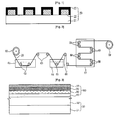
- Fig. 1 is a cross-sectional diagram of an EMI(electromagnetic interference) shielding film comprising the conductive pattern according to the present invention
- Fig. 2 is a schematic diagram illustrating the blackening processing, washing and drying steps of the EMI(electromagnetic interference) shielding film according to the present invention.
- Fig. 3 is a cross-sectional diagram of an optical filter for a display device comprising the EMI(electromagnetic interference) shielding film according to the present invention.
- the method for preparing a conductive pattern, and the conductive pattern prepared therefrom, according to the present invention have applications in various fields.
- the present invention will be specifically explained with reference to an EMI(electromagnetic interference) shielding film.
- the EMI(electromagnetic interference) shielding film (20) comprises a substrate (21), a conductive pattern (22) formed on the substrate (21), and a blackened layer (23) formed on the surface of the conductive pattern (22), as shown in Fig. 1 .
- the EMI(electromagnetic interference) shielding film (20) is prepared by carrying out a step of preparing a substrate (21); a pattern forming step of forming conductive pattern (22) made from metal materials on a substrate (21); and a blackening processing step of blackening the surface of the conductive pattern (22) by immersing the conductive pattern (22) in an aqueous solution containing the reducing metal ions for a predetermined time.
- a washing step of washing the blackened conductive pattern (22); and a drying step of drying the washed conductive pattern (22) for a predetermined time can be further carried out.
- the substrate (21) is made from materials having excellent adhesiveness and light transmittance, and can be formed of at least one resin selected from a polyacrylic resin, a polyurethane resin, a polyester resin, a polyepoxy resin, a polyolefin resin, a polycarbonate resin and a cellulose resin.
- the substrate (21) is preferably formed of transparent PET (polyethyleneterephthalate).
- the conductive paste is printed on the substrate (21) in the off-set printing method, and a conductive pattern (22) is formed on the substrate (21).
- the off-set printing method is used in the pattern forming step of forming the conductive pattern (22) on the substrate (21), but photolithography can also be used.
- the conductive paste is formed by dispersing metal powders in a suitable organic solvent, and a polymeric binder can be added to the organic solvent.
- the metal powders are powdered metals having high electric conductivity, and include various metals, in addition to silver, copper, gold and aluminum, among which silver powders having the lowest specific resistance are most preferred.
- butyl carbitol acetate, carbitol acetate, cyclohexanone, cellosolve acetate, terpineol, or the like can be used as the organic solvent.
- the polymeric binder is added in order to function to allow the conductive paste to have a viscosity suitable for off-set printing, as well as to improve the adhesiveness between the conductive pattern (22) and the substrate (21), provided by the conductive paste.
- the polymeric binder include various materials similar to the substrate (21), in addition to a polyacrylic resin, a polyurethane resin, a polyester resin, a polyepoxy resin, a polyolefin resin, a polycarbonate resin, and a cellulose resin.
- the method involves the steps of: filling a conductive paste in the concave part on a concave plate; transferring the conductive paste from the concave part of a concave plate to a printing blanket by contacting the printing blanket with the concave plate; and forming a conductive pattern (22) on the substrate (21) by contacting the printing blanket with the substrate (21), and transferring the conductive paste from the printing blanket to substrate (21).
- the conductive paste can be injected to the concave part to fill the conductive paste in the concave part, the conductive paste is applied on the entire concave plate, and then the remaining part is scratched with a blade to leave the conductive paste only on the concave part and to fill the conductive paste in the concave part.
- the invention is explained with reference to the concave plate off-set printing method, but a flat plate off-set printing method or a convex plate off-set printing method can be used.
- the conductive paste is directly printed on the substrate (21), but another resin is coated on the substrate (21) to improve the adhesiveness between the conductive paste and the substrate (21), and then the conductive paste is printed.
- the EMI(electromagnetic interference) shielding film (20) is wound up onto a first take-up roller (60).
- the conductive pattern (22) formed by the off-set printing method is immersed in an aqueous solution containing the reducing metal ions for 3 to 300 seconds. That is, the EMI(electromagnetic interference) shielding film (20) wound up onto the first take-up roller (60) is transported to the blackening processing bath (61) having an aqueous solution containing the reducing metal ions received therein via a blackening processing roller (62), and then immersed in the aqueous solution containing the reducing metal ions in the blackening processing bath (61) for 3 to 300 seconds. Thus, the surface of the conductive pattern (22) is oxidized and becomes black.
- the conductive pattern (22) can be blackened by suitably controlling the immersion time. If the immersion time is too short, a desired degree of blackness is not easily obtained, while if the immersion time is too long, the productivity is lowered. Accordingly, the immersion time is 3 to 300 seconds, more preferably 10 to 60 seconds.
- the EMI(electromagnetic interference) shielding film (20) which has been completely blackened in the blackening processing bath (61), as shown in Fig. 2 is guided to a washing step using a washing treatment bath (64) by a first guide roller (63), and the EMI(electromagnetic interference) shielding film (20) is introduced to the washing treatment bath (64) having a washing liquid received therein by a washing treatment roller (65), and then washed therein.
- the EMI(electromagnetic interference) shielding film (20) washed in the washing treatment bath (64) is guided to a drying step using a drying treatment bath (67) by a second guide roller (66), and the EMI(electromagnetic interference) shielding film (20) is introduced to the drying treatment bath (67) by a drying treatment roller (68), dried therein, and finally wound up onto a second take-up roller (69) for storage.
- drying is preferably carried out at a drying temperature of 50 to 120°C for 3 to 10 minutes, most preferably at 70°C for 5 minutes. If the drying temperature is excessively higher than 120°C, the substrate (21) of the EMI(electromagnetic interference) shielding film (20) may be deformed, while if the drying temperature is excessively lower than 50°C, the drying time becomes longer, whereby the productivity may be deteriorated.
- the drying treatment bath (67) may be provided in the form of an oven for directly applying heat onto the EMI(electromagnetic interference) shielding film (20), or in the form of a hot-air spray device for spraying hot air onto the eEMI(electromagnetic interference) shielding film (20).
- the drying treatment bath (67) may be provided in the form of a heater in which the drying treatment roller (68) in the drying treatment bath (67) emits heat itself, but not limited thereto.
- a silver(Ag) conductive pattern is used as the conductive pattern (22), and an aqueous FeCl 3 solution, an aqueous K 3 Fe(CN) 6 solution, and an aqueous CuCl 2 solution are used as the aqueous solutions comprising the reducing metal ions.
- the degrees of blackness (L values) and the sheet resistances ( ⁇ / ⁇ ) are summarized in Table 1.
- the sheet resistance is increased, and the conductive pattern exhibits high sheet resistance, meaning that the conductance is lowered, and the EMI(electromagnetic interference) shielding ability is also lowered.
- the sheet resistance of the silver(Ag) conductive pattern before blackening processing was 0.35 ⁇ / ⁇ .
- the sheet resistance of the silver(Ag) conductive pattern before blackening processing was 0.35 ⁇ / ⁇ .
- the sheet resistance was not increased, and the sheet resistance was decreased to 0.17,0.33, and 0.21 ⁇ / ⁇ , respectively.
- the smaller degrees of blackness (L values) mean the greater intensities of blackness.
- the degrees of blackness (L value) of the silver(Ag) conductive pattern after blackening processing were remarkably decreased to 31.8, 37.6, and 27.1, as compared with 66.6, 63.8, and 66.3 of the degrees of blackness (L value) of the silver(Ag) conductive pattern before blackening processing. From this, it was confirmed that the silver(Ag) conductive pattern (22) is sufficiently blackened.
- a concentrated nitric acid solution comprising 10% by weight of nitric acid and balance q. s. to 100% by weight of water, based on the total weight, was prepared. Then, a silver(Ag) conductive pattern was immersed in the concentrated nitric acid solution for 30 seconds, and the results thereof are shown in Table 2.
- the degree of blackness (L value) was 55.5, and the pattern was not sufficiently blackened, as compared with 67.2 of the degree of blackness (L value) before blackening processing with the concentrated nitric acid solution. Further, it is also found that the values were larger, as compared with 31.8, 37.6, and 27.1 of the degrees of blackness (L values) in Examples 1 to 3 of the present invention. That is, if the concentrated nitric acid solution was used, the pattern was not sufficiently blackened, as compared with the present invention. Further, even if the pattern was immersed in the concentrated nitric acid solution for 20 minutes or longer, it was not likely to obtain a desired degree blackness.
- Example 1 to 3 an aqueous solution containing the reducing metal ions such as an aqueous FeCl 3 solution, an aqueous CuCl 2 Solution and an aqueous K 3 Fe(CN) 6 Solution was used, the sheet resistance after blackening processing was reduced.
- Table 2 it was confirmed that if blackening processing with a concentrated nitric acid solution is carried out, the sheet resistance was significantly increased from 0.35 ⁇ / ⁇ of the sheet resistance before blackening processing to 0.44 ⁇ / ⁇ of the sheet resistance after blackening processing.
- the sheet resistance after blackening processing is not higher than that before blackening processing, and the sheet resistance is also reduced, whereby the silver(Ag) conductive pattern can be sufficiently blackened, and a further enhanced degree of blackness can be obtained, as compared with that by the blackening processing method of the silver(Ag) conductive pattern using a concentrated nitric acid solution.
- the surface of the silver(Ag) conductive pattern is oxidized by reduction of Fe or Cu, a lower degree of blackness (L value) can be obtained. That is, the pattern can be significantly blackened.
- the aqueous solution further contains Cl ions, AgCl crystals are formed on the surface of the silver(Ag) conductive pattern by the Cl ions, and thus the size of the conductive crystal (AgCl crystals) is increased, whereby the sheet resistance is not increased, but decreased.
- the conductance is enhanced, whereby the EMI(electromagnetic interference) shielding ability can be enhanced.
- a conductive paste is printed on the substrate (21) by an off-set printing method, the conductive pattern (22) can be conveniently formed on the substrate (21), allowing easy preparation of the conductive pattern, whereby the productivity is enhanced, and the production cost is reduced.
- blackening processing step (22) becomes easier, whereby the productivity can be enhanced, and the production cost can be reduced.
- the EMI(electromagnetic interference) shielding film (20) prepared by the above-described preparation method can be applied on the optical filter (100) disposed in front of the display panel of a display device.
- the optical filter (100) disposed in front of the plasma display panel (50) having a rear panel (51) and a front panel (52), comprises a color correction film (40) for enhancing the color purity through control of the shade by incorporation of a color adjusting dye; a near infrared ray shielding film (30) laminated on the color correction film (40), for shielding the near infrared ray generated in the plasma display panel (50) for prevention of misoperation of an electronic instrument such as a remote controller; an EMI(electromagnetic interference) shielding film (20) according to the present invention laminated on the near infrared ray shielding film (30), for shielding the EMI(electromagnetic interference) generated in the plasma display panel (50); and an anti-reflection film (10) laminated on the EMI(electromagnetic interference) shielding film (20), for preventing the external light incident from the outside from be reflected outward again.
- a color correction film (40) for enhancing the color purity through control of the shade by incorpor
- the optical filter (100) applied with the EMI(electromagnetic interference) shielding film (20) according to the present invention is disposed in front of the plasma display panel (50), the light emitted from the plasma display panel (50) by gloss of the conductive pattern made from the metallic materials and the outer light are reflected, whereby reduction of the contrast ratio of the display device is prevented by a blackened layer (23) formed on the conductive pattern (22) of the EMI(electromagnetic interference) shielding film (20).
- the display panel is described with reference to the plasma display panel (50), but is not limited thereto.
- the optical filter (100) to be disposed in front of the plasma display panel (50)
- the color correction film (40), the near infrared ray shielding film (30), the EMI(electromagnetic interference) shielding film (20), and the anti-reflection film (10) are laminated in this order, but the lamination order is not limited thereto.
Landscapes
- Chemical & Material Sciences (AREA)
- Engineering & Computer Science (AREA)
- Physics & Mathematics (AREA)
- Materials Engineering (AREA)
- Chemical Kinetics & Catalysis (AREA)
- Mechanical Engineering (AREA)
- Metallurgy (AREA)
- Organic Chemistry (AREA)
- General Chemical & Material Sciences (AREA)
- Microelectronics & Electronic Packaging (AREA)
- Plasma & Fusion (AREA)
- Spectroscopy & Molecular Physics (AREA)
- General Physics & Mathematics (AREA)
- Optics & Photonics (AREA)
- Shielding Devices Or Components To Electric Or Magnetic Fields (AREA)
- Manufacturing Of Electric Cables (AREA)
- Manufacturing Of Printed Wiring (AREA)
- Devices For Indicating Variable Information By Combining Individual Elements (AREA)
Claims (9)
- Verfahren zur Herstellung eines leitenden Musters, umfassend einen Musterausbildungsschritt der Ausbildung eines leitenden Musters auf einem Substrat; und einen Schwärzungsbearbeitungsschritt der Schwärzung der Oberfläche des leitenden Musters durch Eintauchen des leitenden Musters in eine wässrige Lösung, die reduzierende Metall-Ionen enthält, um die Oberfläche des leitenden Musters zu oxidieren, wobei, im Musterausbildungsschritt, das leitende Muster ein leitendes Muster aus Silber (Ag) ist, erhalten durch direktes Aufdrucken einer leitenden Paste, die Silber(Ag)-Pulver umfasst, auf das Substrat: die wässrige Lösung, die die reduzierende Metall-Ionen enthält., weiter Cl-Ionen enthält; und, im Schwärzungsbearbeitungsschritt, das leitende Muster aus Silber (Ag) in eine wässrige Lösung eingetaucht wird, die Cl-Ionen und die reduzierenden Metall-Ionen enthält, um AgCl-Kristalle auf der Oberfläche des leitenden Musters auszubilden.
- Verfahren zur Herstellung eines leitenden Musters nach Anspruch 1, wobei die wässrige Lösung, die die reduzierenden Metall-Ionen enthält, eine wässrige Lösung ist, die Fe- oder Cu-Ionen als die reduzierenden Metall-Ionen enthält.
- Verfahren zur Herstellung eines leitenden Musters nach Anspruch 1, wobei die wässrige Lösung, die die reduzierenden Metall-Ionen enthält, ausgewählt ist aus einer wässrigen FeCl3-Lösung, einer wässrigen CuCl2-Lösung und einer wässrigen K3Fe(CN)6-Lösung, zugesetzt mit einer Lösung, die Cl-Ionen enthält.
- Verfahren zur Herstellung eines leitenden Musters nach Anspruch 1, wobei, im Schwärzungsbearbeitungsschritt, die wässrige Lösung, die die reduzierenden Metall-Ionen enthält, eine wässrige Lösung ist, die Fe- oder Cu-Ionen als die reduzierenden Metall-Ionen enthält.
- Leitendes Muster, umfassend
eine leitende Musterschicht, ausgebildet auf einem Substrat; und
eine geschwärzte Schicht, ausgebildet auf der Oberfläche der leitenden Musterschicht durch Eintauchen der leitenden Musterschicht in eine wässrige Lösung, die reduzierende Metall-Ionen enthält, zum Oxidieren der Oberfläche der leitenden Musterschicht, wobei die leitende Musterschicht eine leitende Musterschicht aus Silber (Ag) ist, erhalten durch direktes Aufdrucken einer leitenden Paste, die Silber(Ag)-Pulver umfasst, auf das Substrat, die wässrige Lösung, die die reduzierenden Metall-Ionen enthält, weiter Cl-Ionen umfasst und die geschwärzte Schicht ein AgCl-Kristall ist, ausgebildet auf der Oberfläche der leitenden Musterschicht aus Silber (Ag) durch die Cl-Ionen einer wässrigen Lösung. die Cl-Ionen und die reduzierenden Metall-Ionen enthält. - Leitendes Muster nach Anspruch 5, wobei die wässrige Lösung, die die reduzierenden Metall-Ionen enthält, eine wässrige Lösung ist, die Fe- oder Cu-Ionen als die reduzierenden Metall-Ionen enthält.
- Leitendes Muster nach Anspruch 5, wobei die wässrige Lösung, die die reduzierenden Metall-Ionen enthält, ausgewählt ist aus einer wässrigen FeCl3-Lösung, einer wässrigen CuCl2-Lösung und einer wässrigen K3Fe(CN)6-Lösung, zugegeben mit einer Lösung, die Cl-Ionen enthält.
- EMI(elektromagnetische Interferenz)-Abschirmungsfilm, umfassend das leitende Muster nach Anspruch 5.
- Optischer Filter für Displayvorrichtung, umfassend den EMI(elektromagnetische Interferenz)-Abschirmungsfilm nach Anspruch 8.
Applications Claiming Priority (2)
| Application Number | Priority Date | Filing Date | Title |
|---|---|---|---|
| KR20050124866 | 2005-12-16 | ||
| PCT/KR2006/005504 WO2007069870A1 (en) | 2005-12-16 | 2006-12-15 | Method for preparing conductive pattern and conductive pattern prepared by the method |
Publications (3)
| Publication Number | Publication Date |
|---|---|
| EP1960194A1 EP1960194A1 (de) | 2008-08-27 |
| EP1960194A4 EP1960194A4 (de) | 2011-01-26 |
| EP1960194B1 true EP1960194B1 (de) | 2013-08-07 |
Family
ID=38163139
Family Applications (1)
| Application Number | Title | Priority Date | Filing Date |
|---|---|---|---|
| EP06835222.8A Not-in-force EP1960194B1 (de) | 2005-12-16 | 2006-12-15 | Verfahren zur herstellung eines leitenden musters und durch das verfahren hergestelltes leitendes muster |
Country Status (7)
| Country | Link |
|---|---|
| US (1) | US8025953B2 (de) |
| EP (1) | EP1960194B1 (de) |
| JP (1) | JP4802248B2 (de) |
| KR (1) | KR101050137B1 (de) |
| CN (1) | CN101360606B (de) |
| TW (1) | TWI302083B (de) |
| WO (1) | WO2007069870A1 (de) |
Families Citing this family (25)
| Publication number | Priority date | Publication date | Assignee | Title |
|---|---|---|---|---|
| WO2008018413A1 (en) * | 2006-08-08 | 2008-02-14 | Panasonic Corporation | Rfid magnetic sheet, noncontact ic card and portable mobile communication apparatus |
| JP5207728B2 (ja) * | 2006-12-21 | 2013-06-12 | 富士フイルム株式会社 | 導電膜およびその製造方法 |
| KR100864152B1 (ko) * | 2007-04-02 | 2008-10-16 | 주식회사 엘지화학 | 전도성 패턴이 흑화처리된 전자파 차폐 유리 및 그제조방법 |
| KR100965376B1 (ko) * | 2007-08-24 | 2010-06-22 | 삼성코닝정밀소재 주식회사 | 디스플레이 장치용 전자파 차폐 부재 |
| JP5087384B2 (ja) * | 2007-12-14 | 2012-12-05 | 三菱製紙株式会社 | 導電性部材の製造方法および導電性部材 |
| JP5149644B2 (ja) * | 2008-02-15 | 2013-02-20 | パナソニック株式会社 | 黒色化導体パターンの形成方法及び黒色化導体パターン |
| KR101091853B1 (ko) * | 2008-09-17 | 2011-12-12 | 주식회사 엘지화학 | 전도성 패턴의 제조방법 및 이에 의해 제조된 전도성 패턴 |
| US8503123B2 (en) * | 2008-12-30 | 2013-08-06 | Samsung Sdi Co., Ltd. | Optical filter and flat display panel comprising the same |
| JP5418121B2 (ja) * | 2009-10-02 | 2014-02-19 | 大日本印刷株式会社 | 透明導電材 |
| JP5593848B2 (ja) * | 2010-05-31 | 2014-09-24 | 大日本印刷株式会社 | 透明導電材 |
| JP5499925B2 (ja) * | 2010-06-15 | 2014-05-21 | 大日本印刷株式会社 | 透明導電材の製造方法 |
| TWI468104B (zh) * | 2011-08-22 | 2015-01-01 | Ckm Building Material Corp | 電磁波濾阻板材構造 |
| CN103582304B (zh) * | 2012-07-30 | 2016-08-03 | 富葵精密组件(深圳)有限公司 | 透明印刷电路板及其制作方法 |
| KR20140060767A (ko) * | 2012-11-12 | 2014-05-21 | 삼성전기주식회사 | 회로 기판 및 그 제조 방법 |
| TWI552211B (zh) * | 2012-11-30 | 2016-10-01 | 恆顥科技股份有限公司 | 觸控電極裝置 |
| KR20150016119A (ko) | 2013-08-01 | 2015-02-11 | 주식회사 엘지화학 | 투명 전도성 적층체, 투명 전도성 적층체를 포함하는 투명 전극, 및 투명 전도성 적층체의 제조방법 |
| US20160330835A1 (en) * | 2014-01-24 | 2016-11-10 | Toppan Forms Co., Ltd. | Wiring board |
| JP6501300B2 (ja) * | 2014-04-28 | 2019-04-17 | トッパン・フォームズ株式会社 | 積層体の製造方法 |
| JP5862916B1 (ja) * | 2014-06-24 | 2016-02-16 | 奥野製薬工業株式会社 | 銅系金属又は銀系金属の黒化処理用組成物 |
| KR101970494B1 (ko) * | 2014-09-11 | 2019-04-22 | (주)엘지하우시스 | 인테리어 필름 및 그의 제조방법 |
| US10670776B2 (en) | 2015-03-20 | 2020-06-02 | Dai Nippon Printing Co., Ltd. | Antireflection film, display device in which said antireflection film is used, and method for selecting antireflection film |
| JP6539181B2 (ja) * | 2015-10-07 | 2019-07-03 | 株式会社写真化学 | 銀配線の黒化方法及びディスプレイ装置 |
| CN107142634A (zh) * | 2017-05-12 | 2017-09-08 | 江门市慈美科技有限公司 | 一种印膜加工生产线 |
| CN108060415B (zh) * | 2018-01-23 | 2023-09-22 | 山东九佳紧固件股份有限公司 | 一种可烘干工件的发黑处理装置及其处理方法 |
| US10976589B2 (en) | 2018-04-17 | 2021-04-13 | Himax Display, Inc. | Display panel having a patterned light shielding layer protected by a protective structure |
Family Cites Families (22)
| Publication number | Priority date | Publication date | Assignee | Title |
|---|---|---|---|---|
| US4263109A (en) * | 1980-03-31 | 1981-04-21 | Cominco Ltd. | Precipitation of chloride from zinc sulphate solution |
| JPH0634448B2 (ja) * | 1988-07-25 | 1994-05-02 | 株式会社日立製作所 | 多層プリント配線板及びその製造方法 |
| JPH09321443A (ja) | 1996-05-30 | 1997-12-12 | Matsushita Electric Works Ltd | 多層板の製造方法 |
| JP3456108B2 (ja) | 1997-04-22 | 2003-10-14 | 松下電器産業株式会社 | 圧電素子およびその製造方法 |
| KR100335346B1 (ko) * | 1997-11-11 | 2002-06-20 | 이사오 우치가사키 | 전자파차폐성접착필름,이필름을채용한전자파차폐성어셈블리및표시소자 |
| KR100374222B1 (ko) * | 1997-12-24 | 2003-03-04 | 군제 가부시키가이샤 | 전자파 실드용 투명부재 및 그 제조방법 |
| JP2000013088A (ja) | 1998-06-26 | 2000-01-14 | Hitachi Chem Co Ltd | 電磁波シールドフィルムの製造方法および該電磁波シールドフィルムを用いた電磁波遮蔽体、ディスプレイ |
| JP2002299779A (ja) | 2001-03-30 | 2002-10-11 | Hitachi Metals Ltd | 配線形成用帯材及びそれを用いたバンプ付き配線を有する配線板並びに配線形成用帯材を用いた転写配線板の製造方法 |
| JP2002326305A (ja) * | 2001-04-27 | 2002-11-12 | Nisshinbo Ind Inc | 透視性電磁波シールド板、その製造方法及びディスプレイ装置 |
| JP4811756B2 (ja) | 2001-09-28 | 2011-11-09 | Dowaメタルテック株式会社 | 金属−セラミックス接合回路基板の製造方法 |
| CN100346003C (zh) * | 2002-07-12 | 2007-10-31 | 藤森工业株式会社 | 电磁波屏蔽材料及其制造方法 |
| JP4339789B2 (ja) * | 2002-08-08 | 2009-10-07 | 大日本印刷株式会社 | 電磁波遮蔽用シートおよびその製造方法 |
| KR100581856B1 (ko) | 2002-11-20 | 2006-05-22 | 삼성에스디아이 주식회사 | 다용도 필터를 구비한 플라즈마 디스플레이 패널 |
| KR100523126B1 (ko) | 2003-02-12 | 2005-10-19 | 엘지마이크론 주식회사 | 근적외선을 차단할수 있는 디스플레이 장치용 전자파 차폐필터 |
| KR100509764B1 (ko) | 2003-04-10 | 2005-08-25 | 엘지전자 주식회사 | 전자파 차폐 필터 및 그 제조 방법 |
| JPWO2005013664A1 (ja) | 2003-07-30 | 2007-09-27 | 大日本印刷株式会社 | プラズマディスプレイ用前面板、及びプラズマディスプレイ |
| KR100582900B1 (ko) | 2004-06-08 | 2006-05-25 | 엘지마이크론 주식회사 | 금속박막에 흑색산화층을 형성하기 위한 용액, 이를이용한 전자파 차폐필터의 금속박막에 흑색산화층을형성하는 방법 및 이에 의해 형성된 전자파 차폐필터의금속박막 |
| KR100610655B1 (ko) * | 2004-07-05 | 2006-08-10 | 한국철도기술연구원 | 무선을 이용한 열차제어시스템과 고정폐색 연동시스템의인터페이스 장치 및 그 제어방법 |
| KR100780283B1 (ko) * | 2004-09-01 | 2007-11-28 | 삼성코닝 주식회사 | 전자파 차폐 필름 및 이의 제조방법 |
| KR100631344B1 (ko) | 2004-10-11 | 2006-10-09 | 엘지마이크론 주식회사 | 디스플레이 장치용 광학필터 및 그 제조방법 |
| US7749686B2 (en) * | 2005-09-30 | 2010-07-06 | Fujifilm Corporation | Method for producing conductive film and light-sensitive material for conductive film production |
| JP4783721B2 (ja) | 2006-12-08 | 2011-09-28 | 大日本印刷株式会社 | 金属黒化処理方法、電磁波遮蔽フィルタ及び複合フィルタ、並びにディスプレイ |
-
2006
- 2006-12-15 TW TW095147218A patent/TWI302083B/zh active
- 2006-12-15 KR KR1020060128732A patent/KR101050137B1/ko not_active Expired - Fee Related
- 2006-12-15 CN CN2006800514583A patent/CN101360606B/zh not_active Expired - Fee Related
- 2006-12-15 WO PCT/KR2006/005504 patent/WO2007069870A1/en not_active Ceased
- 2006-12-15 US US12/086,613 patent/US8025953B2/en active Active
- 2006-12-15 JP JP2008545499A patent/JP4802248B2/ja active Active
- 2006-12-15 EP EP06835222.8A patent/EP1960194B1/de not_active Not-in-force
Also Published As
| Publication number | Publication date |
|---|---|
| JP4802248B2 (ja) | 2011-10-26 |
| TWI302083B (en) | 2008-10-11 |
| KR101050137B1 (ko) | 2011-07-19 |
| CN101360606A (zh) | 2009-02-04 |
| EP1960194A1 (de) | 2008-08-27 |
| JP2009519607A (ja) | 2009-05-14 |
| US8025953B2 (en) | 2011-09-27 |
| EP1960194A4 (de) | 2011-01-26 |
| CN101360606B (zh) | 2011-04-20 |
| US20090117342A1 (en) | 2009-05-07 |
| WO2007069870A1 (en) | 2007-06-21 |
| KR20070064405A (ko) | 2007-06-20 |
| TW200733868A (en) | 2007-09-01 |
Similar Documents
| Publication | Publication Date | Title |
|---|---|---|
| EP1960194B1 (de) | Verfahren zur herstellung eines leitenden musters und durch das verfahren hergestelltes leitendes muster | |
| CN101512684B (zh) | 导电薄膜及其制备方法 | |
| KR101091853B1 (ko) | 전도성 패턴의 제조방법 및 이에 의해 제조된 전도성 패턴 | |
| JP2009252868A (ja) | 光透過性電磁波シールド材及びその製造方法 | |
| KR101234872B1 (ko) | 도금 방법, 투광성 도전성막 및 전자기파 차폐막 | |
| US7244159B2 (en) | Electromagnetic-shielding transparent window member and method for producing the same | |
| KR100973933B1 (ko) | 흑화처리된 전자파 차폐 유리 및 그 제조방법 | |
| US20120327613A1 (en) | Conductive substrate and method for manufacturing the same | |
| EP2132969B1 (de) | Abschirmungsglas für elektromagnetische interferenz mit schwarzer leitfähiger struktur und herstellungsverfahren dafür | |
| KR20090108944A (ko) | 전도성 패턴의 제조방법 및 이에 의해 제조된 전도성 패턴 | |
| JP5602510B2 (ja) | 透明導電フィルム、それを用いた電磁波シールド材及びタッチセンサー、並びにそれらの製造方法 | |
| KR20140024878A (ko) | 투명 컴포넌트 개선 및 투명 컴포넌트 관련 개선 | |
| JP5499943B2 (ja) | 電磁波遮蔽材の電気抵抗低減化処理を利用した製造方法 | |
| JP6941977B2 (ja) | 透明導電性フィルム及びその製造方法 | |
| JP2001092363A (ja) | ディスプレイ用フィルター | |
| JP2009302084A (ja) | 光透過性電磁波シールド材の製造方法、光透過性電磁波シールド材、およびディスプレイ用フィルタ、並びに導電材料の電気抵抗を低下させる方法 | |
| KR20080019841A (ko) | 전자파차폐필름의 제조방법 및 이에 의해 제조된전자파차폐필름 | |
| JP2009076827A (ja) | 近赤外線・電磁波遮蔽用積層体及びその製造方法 | |
| KR100560673B1 (ko) | 전도성 물질로 전면 및 측면이 처리된 매쉬를 갖는패턴화된 동박 |
Legal Events
| Date | Code | Title | Description |
|---|---|---|---|
| PUAI | Public reference made under article 153(3) epc to a published international application that has entered the european phase |
Free format text: ORIGINAL CODE: 0009012 |
|
| 17P | Request for examination filed |
Effective date: 20080613 |
|
| AK | Designated contracting states |
Kind code of ref document: A1 Designated state(s): AT BE BG CH CY CZ DE DK EE ES FI FR GB GR HU IE IS IT LI LT LU LV MC NL PL PT RO SE SI SK TR |
|
| A4 | Supplementary search report drawn up and despatched |
Effective date: 20101223 |
|
| RIC1 | Information provided on ipc code assigned before grant |
Ipc: G02B 5/20 20060101ALN20101217BHEP Ipc: H05K 9/00 20060101AFI20101217BHEP Ipc: C23C 22/06 20060101ALI20101217BHEP |
|
| DAX | Request for extension of the european patent (deleted) | ||
| REG | Reference to a national code |
Ref country code: DE Ref legal event code: R079 Ref document number: 602006037774 Country of ref document: DE Free format text: PREVIOUS MAIN CLASS: B32B0027060000 Ipc: H05K0009000000 |
|
| GRAP | Despatch of communication of intention to grant a patent |
Free format text: ORIGINAL CODE: EPIDOSNIGR1 |
|
| RIC1 | Information provided on ipc code assigned before grant |
Ipc: C23C 22/58 20060101ALI20120829BHEP Ipc: C23C 22/68 20060101ALI20120829BHEP Ipc: H05K 9/00 20060101AFI20120829BHEP |
|
| GRAS | Grant fee paid |
Free format text: ORIGINAL CODE: EPIDOSNIGR3 |
|
| GRAP | Despatch of communication of intention to grant a patent |
Free format text: ORIGINAL CODE: EPIDOSNIGR1 |
|
| GRAA | (expected) grant |
Free format text: ORIGINAL CODE: 0009210 |
|
| AK | Designated contracting states |
Kind code of ref document: B1 Designated state(s): AT BE BG CH CY CZ DE DK EE ES FI FR GB GR HU IE IS IT LI LT LU LV MC NL PL PT RO SE SI SK TR |
|
| REG | Reference to a national code |
Ref country code: GB Ref legal event code: FG4D |
|
| REG | Reference to a national code |
Ref country code: CH Ref legal event code: EP Ref country code: AT Ref legal event code: REF Ref document number: 626215 Country of ref document: AT Kind code of ref document: T Effective date: 20130815 |
|
| REG | Reference to a national code |
Ref country code: IE Ref legal event code: FG4D |
|
| REG | Reference to a national code |
Ref country code: DE Ref legal event code: R096 Ref document number: 602006037774 Country of ref document: DE Effective date: 20131002 |
|
| REG | Reference to a national code |
Ref country code: AT Ref legal event code: MK05 Ref document number: 626215 Country of ref document: AT Kind code of ref document: T Effective date: 20130807 |
|
| REG | Reference to a national code |
Ref country code: NL Ref legal event code: VDEP Effective date: 20130807 |
|
| REG | Reference to a national code |
Ref country code: LT Ref legal event code: MG4D |
|
| PG25 | Lapsed in a contracting state [announced via postgrant information from national office to epo] |
Ref country code: AT Free format text: LAPSE BECAUSE OF FAILURE TO SUBMIT A TRANSLATION OF THE DESCRIPTION OR TO PAY THE FEE WITHIN THE PRESCRIBED TIME-LIMIT Effective date: 20130807 Ref country code: PT Free format text: LAPSE BECAUSE OF FAILURE TO SUBMIT A TRANSLATION OF THE DESCRIPTION OR TO PAY THE FEE WITHIN THE PRESCRIBED TIME-LIMIT Effective date: 20131209 Ref country code: IS Free format text: LAPSE BECAUSE OF FAILURE TO SUBMIT A TRANSLATION OF THE DESCRIPTION OR TO PAY THE FEE WITHIN THE PRESCRIBED TIME-LIMIT Effective date: 20131207 Ref country code: LT Free format text: LAPSE BECAUSE OF FAILURE TO SUBMIT A TRANSLATION OF THE DESCRIPTION OR TO PAY THE FEE WITHIN THE PRESCRIBED TIME-LIMIT Effective date: 20130807 Ref country code: SE Free format text: LAPSE BECAUSE OF FAILURE TO SUBMIT A TRANSLATION OF THE DESCRIPTION OR TO PAY THE FEE WITHIN THE PRESCRIBED TIME-LIMIT Effective date: 20130807 Ref country code: CY Free format text: LAPSE BECAUSE OF FAILURE TO SUBMIT A TRANSLATION OF THE DESCRIPTION OR TO PAY THE FEE WITHIN THE PRESCRIBED TIME-LIMIT Effective date: 20130626 |
|
| PG25 | Lapsed in a contracting state [announced via postgrant information from national office to epo] |
Ref country code: FI Free format text: LAPSE BECAUSE OF FAILURE TO SUBMIT A TRANSLATION OF THE DESCRIPTION OR TO PAY THE FEE WITHIN THE PRESCRIBED TIME-LIMIT Effective date: 20130807 Ref country code: NL Free format text: LAPSE BECAUSE OF FAILURE TO SUBMIT A TRANSLATION OF THE DESCRIPTION OR TO PAY THE FEE WITHIN THE PRESCRIBED TIME-LIMIT Effective date: 20130807 Ref country code: SI Free format text: LAPSE BECAUSE OF FAILURE TO SUBMIT A TRANSLATION OF THE DESCRIPTION OR TO PAY THE FEE WITHIN THE PRESCRIBED TIME-LIMIT Effective date: 20130807 Ref country code: BE Free format text: LAPSE BECAUSE OF FAILURE TO SUBMIT A TRANSLATION OF THE DESCRIPTION OR TO PAY THE FEE WITHIN THE PRESCRIBED TIME-LIMIT Effective date: 20130807 Ref country code: GR Free format text: LAPSE BECAUSE OF FAILURE TO SUBMIT A TRANSLATION OF THE DESCRIPTION OR TO PAY THE FEE WITHIN THE PRESCRIBED TIME-LIMIT Effective date: 20131108 Ref country code: ES Free format text: LAPSE BECAUSE OF FAILURE TO SUBMIT A TRANSLATION OF THE DESCRIPTION OR TO PAY THE FEE WITHIN THE PRESCRIBED TIME-LIMIT Effective date: 20130807 Ref country code: LV Free format text: LAPSE BECAUSE OF FAILURE TO SUBMIT A TRANSLATION OF THE DESCRIPTION OR TO PAY THE FEE WITHIN THE PRESCRIBED TIME-LIMIT Effective date: 20130807 Ref country code: PL Free format text: LAPSE BECAUSE OF FAILURE TO SUBMIT A TRANSLATION OF THE DESCRIPTION OR TO PAY THE FEE WITHIN THE PRESCRIBED TIME-LIMIT Effective date: 20130807 |
|
| PG25 | Lapsed in a contracting state [announced via postgrant information from national office to epo] |
Ref country code: CY Free format text: LAPSE BECAUSE OF FAILURE TO SUBMIT A TRANSLATION OF THE DESCRIPTION OR TO PAY THE FEE WITHIN THE PRESCRIBED TIME-LIMIT Effective date: 20130807 |
|
| PG25 | Lapsed in a contracting state [announced via postgrant information from national office to epo] |
Ref country code: CZ Free format text: LAPSE BECAUSE OF FAILURE TO SUBMIT A TRANSLATION OF THE DESCRIPTION OR TO PAY THE FEE WITHIN THE PRESCRIBED TIME-LIMIT Effective date: 20130807 Ref country code: EE Free format text: LAPSE BECAUSE OF FAILURE TO SUBMIT A TRANSLATION OF THE DESCRIPTION OR TO PAY THE FEE WITHIN THE PRESCRIBED TIME-LIMIT Effective date: 20130807 Ref country code: DK Free format text: LAPSE BECAUSE OF FAILURE TO SUBMIT A TRANSLATION OF THE DESCRIPTION OR TO PAY THE FEE WITHIN THE PRESCRIBED TIME-LIMIT Effective date: 20130807 Ref country code: RO Free format text: LAPSE BECAUSE OF FAILURE TO SUBMIT A TRANSLATION OF THE DESCRIPTION OR TO PAY THE FEE WITHIN THE PRESCRIBED TIME-LIMIT Effective date: 20130807 Ref country code: SK Free format text: LAPSE BECAUSE OF FAILURE TO SUBMIT A TRANSLATION OF THE DESCRIPTION OR TO PAY THE FEE WITHIN THE PRESCRIBED TIME-LIMIT Effective date: 20130807 |
|
| PG25 | Lapsed in a contracting state [announced via postgrant information from national office to epo] |
Ref country code: IT Free format text: LAPSE BECAUSE OF FAILURE TO SUBMIT A TRANSLATION OF THE DESCRIPTION OR TO PAY THE FEE WITHIN THE PRESCRIBED TIME-LIMIT Effective date: 20130807 |
|
| PLBE | No opposition filed within time limit |
Free format text: ORIGINAL CODE: 0009261 |
|
| STAA | Information on the status of an ep patent application or granted ep patent |
Free format text: STATUS: NO OPPOSITION FILED WITHIN TIME LIMIT |
|
| 26N | No opposition filed |
Effective date: 20140508 |
|
| REG | Reference to a national code |
Ref country code: CH Ref legal event code: PL |
|
| REG | Reference to a national code |
Ref country code: DE Ref legal event code: R097 Ref document number: 602006037774 Country of ref document: DE Effective date: 20140508 |
|
| PG25 | Lapsed in a contracting state [announced via postgrant information from national office to epo] |
Ref country code: MC Free format text: LAPSE BECAUSE OF FAILURE TO SUBMIT A TRANSLATION OF THE DESCRIPTION OR TO PAY THE FEE WITHIN THE PRESCRIBED TIME-LIMIT Effective date: 20130807 Ref country code: LU Free format text: LAPSE BECAUSE OF FAILURE TO SUBMIT A TRANSLATION OF THE DESCRIPTION OR TO PAY THE FEE WITHIN THE PRESCRIBED TIME-LIMIT Effective date: 20131215 |
|
| REG | Reference to a national code |
Ref country code: IE Ref legal event code: MM4A |
|
| PG25 | Lapsed in a contracting state [announced via postgrant information from national office to epo] |
Ref country code: IE Free format text: LAPSE BECAUSE OF NON-PAYMENT OF DUE FEES Effective date: 20131215 Ref country code: CH Free format text: LAPSE BECAUSE OF NON-PAYMENT OF DUE FEES Effective date: 20131231 Ref country code: LI Free format text: LAPSE BECAUSE OF NON-PAYMENT OF DUE FEES Effective date: 20131231 |
|
| PG25 | Lapsed in a contracting state [announced via postgrant information from national office to epo] |
Ref country code: TR Free format text: LAPSE BECAUSE OF FAILURE TO SUBMIT A TRANSLATION OF THE DESCRIPTION OR TO PAY THE FEE WITHIN THE PRESCRIBED TIME-LIMIT Effective date: 20130807 |
|
| PG25 | Lapsed in a contracting state [announced via postgrant information from national office to epo] |
Ref country code: HU Free format text: LAPSE BECAUSE OF FAILURE TO SUBMIT A TRANSLATION OF THE DESCRIPTION OR TO PAY THE FEE WITHIN THE PRESCRIBED TIME-LIMIT; INVALID AB INITIO Effective date: 20061215 Ref country code: BG Free format text: LAPSE BECAUSE OF FAILURE TO SUBMIT A TRANSLATION OF THE DESCRIPTION OR TO PAY THE FEE WITHIN THE PRESCRIBED TIME-LIMIT Effective date: 20130807 |
|
| REG | Reference to a national code |
Ref country code: FR Ref legal event code: PLFP Year of fee payment: 10 |
|
| REG | Reference to a national code |
Ref country code: FR Ref legal event code: PLFP Year of fee payment: 11 |
|
| REG | Reference to a national code |
Ref country code: FR Ref legal event code: PLFP Year of fee payment: 12 |
|
| PGFP | Annual fee paid to national office [announced via postgrant information from national office to epo] |
Ref country code: GB Payment date: 20231120 Year of fee payment: 18 |
|
| PGFP | Annual fee paid to national office [announced via postgrant information from national office to epo] |
Ref country code: FR Payment date: 20231121 Year of fee payment: 18 Ref country code: DE Payment date: 20231120 Year of fee payment: 18 |
|
| REG | Reference to a national code |
Ref country code: DE Ref legal event code: R119 Ref document number: 602006037774 Country of ref document: DE |
|
| GBPC | Gb: european patent ceased through non-payment of renewal fee |
Effective date: 20241215 |
|
| PG25 | Lapsed in a contracting state [announced via postgrant information from national office to epo] |
Ref country code: DE Free format text: LAPSE BECAUSE OF NON-PAYMENT OF DUE FEES Effective date: 20250701 |
|
| PG25 | Lapsed in a contracting state [announced via postgrant information from national office to epo] |
Ref country code: GB Free format text: LAPSE BECAUSE OF NON-PAYMENT OF DUE FEES Effective date: 20241215 |
|
| PG25 | Lapsed in a contracting state [announced via postgrant information from national office to epo] |
Ref country code: FR Free format text: LAPSE BECAUSE OF NON-PAYMENT OF DUE FEES Effective date: 20241231 |