EP1962331A2 - Dünnschichtige Solarzelle und Verfahren zu ihrer Herstellung - Google Patents
Dünnschichtige Solarzelle und Verfahren zu ihrer Herstellung Download PDFInfo
- Publication number
- EP1962331A2 EP1962331A2 EP08101896A EP08101896A EP1962331A2 EP 1962331 A2 EP1962331 A2 EP 1962331A2 EP 08101896 A EP08101896 A EP 08101896A EP 08101896 A EP08101896 A EP 08101896A EP 1962331 A2 EP1962331 A2 EP 1962331A2
- Authority
- EP
- European Patent Office
- Prior art keywords
- solar cell
- layer
- thin
- cell layer
- transparent conductive
- Prior art date
- Legal status (The legal status is an assumption and is not a legal conclusion. Google has not performed a legal analysis and makes no representation as to the accuracy of the status listed.)
- Withdrawn
Links
Images






Classifications
-
- H—ELECTRICITY
- H10—SEMICONDUCTOR DEVICES; ELECTRIC SOLID-STATE DEVICES NOT OTHERWISE PROVIDED FOR
- H10F—INORGANIC SEMICONDUCTOR DEVICES SENSITIVE TO INFRARED RADIATION, LIGHT, ELECTROMAGNETIC RADIATION OF SHORTER WAVELENGTH OR CORPUSCULAR RADIATION
- H10F77/00—Constructional details of devices covered by this subclass
- H10F77/95—Circuit arrangements
- H10F77/953—Circuit arrangements for devices having potential barriers
- H10F77/955—Circuit arrangements for devices having potential barriers for photovoltaic devices
-
- H—ELECTRICITY
- H10—SEMICONDUCTOR DEVICES; ELECTRIC SOLID-STATE DEVICES NOT OTHERWISE PROVIDED FOR
- H10F—INORGANIC SEMICONDUCTOR DEVICES SENSITIVE TO INFRARED RADIATION, LIGHT, ELECTROMAGNETIC RADIATION OF SHORTER WAVELENGTH OR CORPUSCULAR RADIATION
- H10F19/00—Integrated devices, or assemblies of multiple devices, comprising at least one photovoltaic cell covered by group H10F10/00, e.g. photovoltaic modules
- H10F19/30—Integrated devices, or assemblies of multiple devices, comprising at least one photovoltaic cell covered by group H10F10/00, e.g. photovoltaic modules comprising thin-film photovoltaic cells
- H10F19/31—Integrated devices, or assemblies of multiple devices, comprising at least one photovoltaic cell covered by group H10F10/00, e.g. photovoltaic modules comprising thin-film photovoltaic cells having multiple laterally adjacent thin-film photovoltaic cells deposited on the same substrate
- H10F19/33—Patterning processes to connect the photovoltaic cells, e.g. laser cutting of conductive or active layers
-
- H—ELECTRICITY
- H10—SEMICONDUCTOR DEVICES; ELECTRIC SOLID-STATE DEVICES NOT OTHERWISE PROVIDED FOR
- H10F—INORGANIC SEMICONDUCTOR DEVICES SENSITIVE TO INFRARED RADIATION, LIGHT, ELECTROMAGNETIC RADIATION OF SHORTER WAVELENGTH OR CORPUSCULAR RADIATION
- H10F10/00—Individual photovoltaic cells, e.g. solar cells
- H10F10/10—Individual photovoltaic cells, e.g. solar cells having potential barriers
-
- H—ELECTRICITY
- H10—SEMICONDUCTOR DEVICES; ELECTRIC SOLID-STATE DEVICES NOT OTHERWISE PROVIDED FOR
- H10F—INORGANIC SEMICONDUCTOR DEVICES SENSITIVE TO INFRARED RADIATION, LIGHT, ELECTROMAGNETIC RADIATION OF SHORTER WAVELENGTH OR CORPUSCULAR RADIATION
- H10F10/00—Individual photovoltaic cells, e.g. solar cells
- H10F10/10—Individual photovoltaic cells, e.g. solar cells having potential barriers
- H10F10/17—Photovoltaic cells having only PIN junction potential barriers
- H10F10/172—Photovoltaic cells having only PIN junction potential barriers comprising multiple PIN junctions, e.g. tandem cells
-
- H—ELECTRICITY
- H10—SEMICONDUCTOR DEVICES; ELECTRIC SOLID-STATE DEVICES NOT OTHERWISE PROVIDED FOR
- H10F—INORGANIC SEMICONDUCTOR DEVICES SENSITIVE TO INFRARED RADIATION, LIGHT, ELECTROMAGNETIC RADIATION OF SHORTER WAVELENGTH OR CORPUSCULAR RADIATION
- H10F19/00—Integrated devices, or assemblies of multiple devices, comprising at least one photovoltaic cell covered by group H10F10/00, e.g. photovoltaic modules
- H10F19/30—Integrated devices, or assemblies of multiple devices, comprising at least one photovoltaic cell covered by group H10F10/00, e.g. photovoltaic modules comprising thin-film photovoltaic cells
- H10F19/31—Integrated devices, or assemblies of multiple devices, comprising at least one photovoltaic cell covered by group H10F10/00, e.g. photovoltaic modules comprising thin-film photovoltaic cells having multiple laterally adjacent thin-film photovoltaic cells deposited on the same substrate
-
- H—ELECTRICITY
- H10—SEMICONDUCTOR DEVICES; ELECTRIC SOLID-STATE DEVICES NOT OTHERWISE PROVIDED FOR
- H10F—INORGANIC SEMICONDUCTOR DEVICES SENSITIVE TO INFRARED RADIATION, LIGHT, ELECTROMAGNETIC RADIATION OF SHORTER WAVELENGTH OR CORPUSCULAR RADIATION
- H10F19/00—Integrated devices, or assemblies of multiple devices, comprising at least one photovoltaic cell covered by group H10F10/00, e.g. photovoltaic modules
- H10F19/40—Integrated devices, or assemblies of multiple devices, comprising at least one photovoltaic cell covered by group H10F10/00, e.g. photovoltaic modules comprising photovoltaic cells in a mechanically stacked configuration
-
- H—ELECTRICITY
- H10—SEMICONDUCTOR DEVICES; ELECTRIC SOLID-STATE DEVICES NOT OTHERWISE PROVIDED FOR
- H10F—INORGANIC SEMICONDUCTOR DEVICES SENSITIVE TO INFRARED RADIATION, LIGHT, ELECTROMAGNETIC RADIATION OF SHORTER WAVELENGTH OR CORPUSCULAR RADIATION
- H10F71/00—Manufacture or treatment of devices covered by this subclass
-
- H—ELECTRICITY
- H10—SEMICONDUCTOR DEVICES; ELECTRIC SOLID-STATE DEVICES NOT OTHERWISE PROVIDED FOR
- H10F—INORGANIC SEMICONDUCTOR DEVICES SENSITIVE TO INFRARED RADIATION, LIGHT, ELECTROMAGNETIC RADIATION OF SHORTER WAVELENGTH OR CORPUSCULAR RADIATION
- H10F77/00—Constructional details of devices covered by this subclass
- H10F77/10—Semiconductor bodies
- H10F77/16—Material structures, e.g. crystalline structures, film structures or crystal plane orientations
- H10F77/169—Thin semiconductor films on metallic or insulating substrates
-
- H—ELECTRICITY
- H10—SEMICONDUCTOR DEVICES; ELECTRIC SOLID-STATE DEVICES NOT OTHERWISE PROVIDED FOR
- H10F—INORGANIC SEMICONDUCTOR DEVICES SENSITIVE TO INFRARED RADIATION, LIGHT, ELECTROMAGNETIC RADIATION OF SHORTER WAVELENGTH OR CORPUSCULAR RADIATION
- H10F77/00—Constructional details of devices covered by this subclass
- H10F77/10—Semiconductor bodies
- H10F77/16—Material structures, e.g. crystalline structures, film structures or crystal plane orientations
- H10F77/169—Thin semiconductor films on metallic or insulating substrates
- H10F77/1694—Thin semiconductor films on metallic or insulating substrates the films including Group I-III-VI materials, e.g. CIS or CIGS
-
- H—ELECTRICITY
- H10—SEMICONDUCTOR DEVICES; ELECTRIC SOLID-STATE DEVICES NOT OTHERWISE PROVIDED FOR
- H10F—INORGANIC SEMICONDUCTOR DEVICES SENSITIVE TO INFRARED RADIATION, LIGHT, ELECTROMAGNETIC RADIATION OF SHORTER WAVELENGTH OR CORPUSCULAR RADIATION
- H10F77/00—Constructional details of devices covered by this subclass
- H10F77/10—Semiconductor bodies
- H10F77/16—Material structures, e.g. crystalline structures, film structures or crystal plane orientations
- H10F77/169—Thin semiconductor films on metallic or insulating substrates
- H10F77/1696—Thin semiconductor films on metallic or insulating substrates the films including Group II-VI materials, e.g. CdTe or CdS
-
- Y—GENERAL TAGGING OF NEW TECHNOLOGICAL DEVELOPMENTS; GENERAL TAGGING OF CROSS-SECTIONAL TECHNOLOGIES SPANNING OVER SEVERAL SECTIONS OF THE IPC; TECHNICAL SUBJECTS COVERED BY FORMER USPC CROSS-REFERENCE ART COLLECTIONS [XRACs] AND DIGESTS
- Y02—TECHNOLOGIES OR APPLICATIONS FOR MITIGATION OR ADAPTATION AGAINST CLIMATE CHANGE
- Y02E—REDUCTION OF GREENHOUSE GAS [GHG] EMISSIONS, RELATED TO ENERGY GENERATION, TRANSMISSION OR DISTRIBUTION
- Y02E10/00—Energy generation through renewable energy sources
- Y02E10/50—Photovoltaic [PV] energy
- Y02E10/541—CuInSe2 material PV cells
-
- Y—GENERAL TAGGING OF NEW TECHNOLOGICAL DEVELOPMENTS; GENERAL TAGGING OF CROSS-SECTIONAL TECHNOLOGIES SPANNING OVER SEVERAL SECTIONS OF THE IPC; TECHNICAL SUBJECTS COVERED BY FORMER USPC CROSS-REFERENCE ART COLLECTIONS [XRACs] AND DIGESTS
- Y02—TECHNOLOGIES OR APPLICATIONS FOR MITIGATION OR ADAPTATION AGAINST CLIMATE CHANGE
- Y02E—REDUCTION OF GREENHOUSE GAS [GHG] EMISSIONS, RELATED TO ENERGY GENERATION, TRANSMISSION OR DISTRIBUTION
- Y02E10/00—Energy generation through renewable energy sources
- Y02E10/50—Photovoltaic [PV] energy
- Y02E10/548—Amorphous silicon PV cells
-
- Y—GENERAL TAGGING OF NEW TECHNOLOGICAL DEVELOPMENTS; GENERAL TAGGING OF CROSS-SECTIONAL TECHNOLOGIES SPANNING OVER SEVERAL SECTIONS OF THE IPC; TECHNICAL SUBJECTS COVERED BY FORMER USPC CROSS-REFERENCE ART COLLECTIONS [XRACs] AND DIGESTS
- Y02—TECHNOLOGIES OR APPLICATIONS FOR MITIGATION OR ADAPTATION AGAINST CLIMATE CHANGE
- Y02P—CLIMATE CHANGE MITIGATION TECHNOLOGIES IN THE PRODUCTION OR PROCESSING OF GOODS
- Y02P70/00—Climate change mitigation technologies in the production process for final industrial or consumer products
- Y02P70/50—Manufacturing or production processes characterised by the final manufactured product
Definitions
- the present invention relates to an integrated thin-film solar cell module and a method of manufacturing the same, and more particularly, to a thin-film solar cell and a method of manufacturing the same, which are capable of improving a photoelectric conversion efficiency.
- materials for solar cells include a pn structure including back electrode layer; a pin structure; a heterojunction structure; a schottky structure; and a multiple junction structure including tandem or vertical junction type.
- a solar cell using monocrystalline bulk silicon which is being commonly used at present, has a high photoelectric conversion efficiency, but the fact is that it is not being actively utilized due to high production and installation costs thereof.
- Research into thin-film solar cells has been actively carried out to solve such problems.
- a thin-film solar cell using amorphous silicon (a-Si:H) which is capable of reducing production costs of large size solar cell modules and energy recovery period, has drawn more attention.
- the thin-film solar cell has problems such that the photoelectric conversion efficiency thereof is lower than that of a monocrystalline silicon solar cell and the efficiency is decreased when exposed to light.
- a structure including semiconductor layers having the different band gap energy and a buffer layer formed therebetween has been suggested to improve the above problems such as the low photoelectric conversion efficiency of the thin-film solar cell using amorphous silicon.
- a-Si:H amorphous silicon
- uc-Si:H microcrystalline silicon
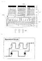
- Fig. 1 is a sectional view illustrating a stack structure of a thin-film solar cell module according to an example of the prior art.
- a first solar cell layer 120 and a second solar cell layer 130 with the different characteristics and crystal structure consist of a stack structure and are electrically connected in series by connecting a transparent conductive layer 111 stacked on the unit cell of the second solar cell 130 with a transparent conductive layer 110 stacked under the adjacent unit cell of the first solar cell layer 120.
- Fig. 2 is an equivalent circuit diagram of a diode illustrating a series connection of the semiconductor layers.
- a first solar cell layer toward incident sunlight consists of amorphous silicon and has a high band gap energy of about 1.7 to 1.9 eV
- a second solar cell layer stacked onto the first solar cell layer consists of microcrystalline silicon and has a band gap energy of about 1.1 eV.
- the thin-film solar cell formed of both solar cell layers has a higher photoelectric conversion efficiency as compared with the thin-film solar cell formed of single solar cell layers.
- the solar cell structure on which the different double solar cell layers are stacked causes a problem such that the current of both the solar cell layers should be designed to be equal because both the solar cell layers are connected in series.
- the thickness of an amorphous silicon intrinsic semiconductor layer of the first solar cell layer, which is located at the lower part should be thickly formed beyond what is otherwise needed, and in proportion to the thickness, as the electric power rate generated at the amorphous solar cell layer become high, the total efficiency due to the Stabler-Wronski effect is excessively decreased.
- a short-circuit current of the first solar cell layer located at a lower part become small, and thus, as the difference of the short-circuit current between both the solar cell layers is increased, the total efficiency of the element in which two layers are connected in series is reduced compared with the total efficiency achieved by both solar cell layers because the whole short-circuit current is limited by the short-circuit current of the first solar cell layer.
- U.S. publication patent No. 2005/0150542 A1 discloses a solar cell module such that a first solar cell layer 220 and a second solar cell layer 230 are respectively connected to an adjacent cell in series, by separating the first solar cell layer 220 located toward the lower part from the second solar cell layer 230 located toward the upper part by a transparent insulating layer and providing a 4-T structure which draws two terminals from each solar cell layer.
- Fig. 3 is a sectional view illustrating a stack structure of a 4-terminal thin-film solar cell module, which is disclosed in the above U.S. patent, and Fig. 4 is a diode equivalent circuit of the 4-terminal thin-film solar cell module.
- the present invention has been suggested to solve the problems. It is an object of the present invention to provide a thin-film solar cell having a structure, which is capable of improving a photoelectric conversion efficiency and a method of manufacturing a thin-film solar cell, which is capable of reducing fabrication costs compared with the other thin-film silicon solar cells by manufacturing the solar cell through a relatively simple process.
- a thin-film solar cell comprising: a first solar cell layer, in which a plurality of unit cells including photoelectric conversion layers are connected in series; a second solar cell layer, in which a plurality of unit cells including the photoelectric conversion layers are connected in series; and an electrode connector, which connects the first solar cell layer with the second solar cell layer.
- the second solar cell layer has a band gap energy, which is different from the first solar cell layer, and a threshold voltage, which is coincident with the first solar cell layer.
- the photoelectric conversion layers is any one selected from a group consisting of amorphous silicon, microcrystalline silicon, monocrystalline silicon, polycrystalline silicon, amorphous SiC, amorphous SiN, amorphous SiGe, amorphous SiSn, gallium arsenide (GaAs), aluminum gallium arsenide (AlGaAs), indium phosphorus (InP), gallium phosphorus (GaP), copper indium gallium selenide (CIGS), cadmium telluride (CdTe), cadmium sulfide, copper sulfide (Cu 2 S), zinc telluride (ZnTe), Plumbum sulfide (PbS), copper indium diselenide (CulnS
- the first solar cell layer and the second solar cell layer may be any one selected from an amorphous silicon solar cell layer and a microcrystalline silicon solar cell layer.
- the amorphous silicon solar cell layer may be formed such that a p-i-n type amorphous silicon layer is consecutively stacked or a p-n type amorphous silicon layer is consecutively stacked.
- microcrystalline silicon solar cell layer may be formed such that a p-i-n type microcrystalline silicon layer is consecutively stacked or a p-n type microcrystalline silicon layer is consecutively stacked.
- a series connection of the unit cells according to the present invention may be provided with each transparent conductive layer at an upper part and a lower part of the unit cells and is characterized by connecting an upper transparent conductive layer of the unit cells with a lower transparent conductive layer of adjacent unit cells.
- a thin-film solar cell comprises at least one or more electrode connector.
- a electrode connector consists of a lower electrode connector, which connects the lower transparent conductive layer of each unit cell of the first solar cell layer with the lower transparent conductive layer of each unit cell of the second solar cell layer, and an upper electrode connector, which connects the upper transparent conductive layer of each unit cell of the first solar cell layer with the upper transparent conductive layer of each unit cell of the second solar cell layer.
- the first solar cell layer and the second solar cell layer are provided with each transparent conductive layer at the upper part and lower part of the unit cells thereof, and are connected in series by connecting the upper transparent conductive layer of each unit cell with the lower transparent conductive layer of an adjacent unit cell.
- the first solar cell layer and the second solar cell layer connected by the upper and lower electrode connectors have the same width as each other.
- the number of unit cells of the first solar cell layer and the second solar cell layer which are included between at least a couple of the upper electrode connector and lower electrode connector can be adjusted so that the first solar cell layer and the second solar cell layer have the same width as each other.
- each number of the unit cells is previously calculated so that a threshold voltage of the first solar cell layer and the second solar cell layer is the same as each other, thereby determining the patterning of the unit cells of the solar cell.
- stack shapes or arrangements of the first solar cell layer and the second solar cell layer should be not construed as being limited to example embodiments set forth herein, as well as they could be easily achieved by those skilled in the art, and preferably, the first solar cell layer and the second solar cell layer may be vertically stacked with an insulating layer therebetween.
- a method of manufacturing a thin-film solar cell of the present invention comprises the steps of: forming a first solar cell layer by forming a plurality of unit cells including a photoelectric conversion layer and connecting them in series; forming a second solar cell layer by forming a plurality of unit cells including a photoelectric conversion layer and connecting them in series; and electrically connecting the first solar cell layer with the second solar cell layer in parallel.
- the second solar cell layer may have a band gap energy, which is different from the first solar cell layer, and a threshold voltage, which is coincident with the first solar cell layer.
- the thin-flim solar cell of the present invention further comprises the step of forming transparent conductive layers at the upper part and lower part of the unit cells, respectively.
- the unit cells may be patterned by any one selected from a laser scribing method, an optical scribing method, a mechanical scribing method, an etching method using plasma, a wet-type etching method, a dry-type etching method, a lift-off method and a wire mask method.
- the method of manufacturing the thin-film solar cell of the present invention further comprises the step of forming an insulating layer between the first solar cell layer and the second solar cell layer.
- a series connection of the unit cells according to the present invention may be provided with each transparent conductive layer at an upper part and a lower part of the unit cells and is characterized by connecting an upper transparent conductive layer of the unit cells with a lower transparent conductive layer of adjacent unit cells.
- an electrode connector is provided with each transparent conductive layer at the upper part lower part of the unit cells of the first solar cell layer and the second solar cell layer, which are formed by connecting the upper transparent conductive layer of unit cells with the lower transparent conductive layer of an adjacent unit cell in series comprising at least one or more electrode connector, which consists of a lower electrode connector, which connects the lower transparent conductive layer of each unit cell of the first solar cell layer with the lower transparent conductive layer of each unit cell of the second solar cell layer; and an upper electrode connector, which connects the upper transparent conductive layer of each unit cell of the first solar cell layer with the upper transparent conductive layer of each unit cell of the second solar cell layer.
- the first solar cell layer and the second solar cell layer, which are connected by the upper and lower electrode connector have the same width as each other.
- the first solar cell layer and the second solar cell layer according to manufacturing methods of the present invention may be vertically stacked with an insulating layer therebetween, but it should not be construed as being limited to this embodiment and may be embodied in many different forms.
- the first solar cell layer may be formed by consecutively stacking a p-i-n type amorphous silicon layer or a p-n type amorphous silicon layer and the second solar cell layer may be formed by consecutively stacking a p-i-n type microcrystalline silicon layer or a p-n type microcrystalline silicon layer
- a method of manufacturing a thin-film solar cell comprises the steps of: stacking and patterning a lower transparent conductive layer of a first solar cell layer on a substrate; stacking and patterning an amorphous silicon p-i-n layer or amorphous silicon p-n layer on a lower transparent conductive layer of the first solar cell layer; forming an upper transparent conductive layer of the first solar cell layer on the amorphous silicon layer and connecting it with the lower transparent conductive layer; forming at least one or more unit cell of the first solar cell layer by patterning the upper transparent conductive layer; forming an insulating layer on unit cells of the first solar cell layer; stacking and patterning the lower transparent conductive layer of a second solar cell layer on the insulating layer; connecting the lower transparent conductive layer of the first solar cell layer with the lower transparent conductive layer of the second solar cell layer through a lower electrode connector; stacking and patterning a microcrystalline silicon p-i-n layer or a microcrystalline silicon p-n layer on the lower transparent conductive layer on the
- the lower electrode connector and upper electrode connector are formed at a distance so that the first solar cell layer and the second solar cell layer have the same width as each other.
- the lower electrode connector and the upper electrode connector form a pair of electrode connectors and at least one or more electrode connector may be formed at a large area thin-film solar cell.
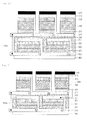
- FIG. 5 is a sectional view illustrating a stack structure of the thin-film solar cell module according to the preferred embodiment of the present invention
- FIG. 6 is a diode equivalent circuit of the thin-film solar cell module according to the preferred embodiment of the present invention.
- the thin-film solar cell is formed by stacking a substrate 300, the first solar cell layer 320, the second solar cell layer 330 and the back-side electrode layer 340; transparent conductive layers 310 and 311 are provided at the lower part and upper part of the first solar cell layer 320, respectively and transparent conductive layers 312 and 313 are provided at the lower part and upper part of the second solar cell layer 330, respectively; and the first solar cell layer 320 and the second solar cell layer 330 are electrically separated from each other by an insulating layer 350 therebetween.
- the example embodiment has a structure that the first solar cell layer 320 and the second solar cell layer 330 may be stacked up and down and provided with the insulating layer therebetween, but is not limited to this structure, thereby there is not any limitation for arrangement shapes of both the solar cell layers.
- Electrically connecting the first solar cell layer 320 with the second solar cell layer 330 in parallel may be carried out by an electrode connector 360a for connecting the lower transparent conductive layer 310 of first solar cell layer 320 and the lower transparent conductive layer 312 of the second solar cell layer 330 and an electrode connector 360b for connecting the upper transparent conductive layer 311 of first solar cell layer 320 and the upper transparent conductive layer 313 of the second solar cell layer 330.
- the upper electrode connector 360b of both the solar cell layers may be connected to a backside electrode layer 340 which is provided at the upper part of the second solar cell layer 330.
- the thin-film solar cell layer consists of a multiple junction structure of a plurality of unit cells separated by patterning and these unit cells are electrically connected in series by the transparent conductive layer formed at the upper part and the lower part of each solar cell layer.
- a plurality of the unit cells are electrically connected in series, thereby forming an integrated large area thin-film solar cell.
- the series connection between the unit cells is achieved through an insulating layer 350 formed between adjacent unit cells.
- the thin-film solar cell has gaps formed between unit cells by patterning from the top and isolation processes, consecutively, to a back-side electrode layer 340, the upper transparent conductive layer 313 and p layer 331 of the second solar cell layer 330, and an air in the gaps can be performed as an insulating layer and adjacent unit cells are electrically connected in series.
- Two solar cell layers consisting of the unit cells, which are connected in series, namely, the first solar cell layer 320 and the second solar cell layer 330 are connected in parallel by the electrode connectors 360a, 360b.
- Semiconductor materials that form the first solar cell layer 320 and the second solar cell layer 330 may be formed of materials, which are different from each other having different characteristics. Namely, they may consist of semiconductor materials having different band gap energy.
- the thin-film solar cell according to the preferred embodiment of the present invention may be formed of amorphous silicon and microcrystalline silicon.
- the first solar cell layer 320 stacked on a glass substrate 300 may be made of amorphous silicon and the second solar cell layer 330 also may be made of microcrystalline silicon.
- a band gap energy of the amorphous silicon semiconductor layer is 1.7eV to 1.9eV and a band gap energy of the microcrystalline silicon semiconductor layer is 1.1eV.
- any one among general semiconductor materials such as amorphous silicon, microcrystalline silicon, monocrystalline silicon, polycrystalline silicon, amorphous SiC, amorphous SiN, amorphous SiGe, amorphous SiSn, gallium arsenide (GaAs), aluminum gallium arsenide (AlGaAs), indium phosphorus (InP), gallium phosphorus (GaP), copper indium gallium selenide (CIGS), cadmium telluride (CdTe), cadmium sulfide, copper sulfide (Cu 2 S), zinc telluride (ZnTe), Plumbum sulfide (PbS), copper indium diselenide (CulnSe 2 ; CIS), gallium antimonide (GaSb) and compounds thereof may be selected.
- general semiconductor materials such as amorphous silicon, microcrystalline silicon, monocrystalline silicon, polycrystalline silicon, amorphous SiC, amorphous SiN, amorphous SiGe
- One solar cell layer may be formed by stacking a semiconductor layer having p-i-n or p-n type junction structure.
- the first solar cell layer 320 stacked on a glass substrate 300 may be formed by stacking a p-type semiconductor layer 321, an i-type semiconductor layer 322, and a n-type semiconductor layer 323.
- the second solar cell layer 330 may be formed by stacking a p-type semiconductor layer 331, an i-type semiconductor layer 332, and a n-type semiconductor layer 333.
- a threshold voltage of unit cell that forms both the solar cell layers is different from each other because the semiconductor materials that form the first solar cell layer and the second solar cell layer are formed of the materials, which are different from each other having the different band gap characteristics.
- the electrode connector when the length that both the solar cell layers are connected in parallel by the electrode connector become one solar cell unit module, it should be configured so that threshold voltages of each solar cell layer within the unit module are nearly coincident with each other. Since the difference between the short-circuit currents is increased and the total efficiency of the solar cell module is reduced by the different band gap energy of semiconductor materials that form each solar cell layer, it is necessary that the threshold voltages of each solar cell layer within the unit module are nearly coincident with each other.
- the number of unit cell that forms each solar cell layer is adjusted and patterned accordingly.
- the number of unit cells of the first solar cell layer provided within a unit module, which is connected in parallel by a pair of electrode connectors is 2 unit cells and the number of unit cells of the second solar cell layer becomes 3 unit cells.
- the threshold voltages of both the solar cell layers are nearly coincident with each other.
- the photoelectric conversion efficiency is not reduced by the difference of the threshold voltage, thereby obtaining the solar cell module having a high efficiency.
- the first solar cell layer and the second solar cell layer within the unit module formed by a couple of electrode connectors have the same width as each other, and thus, the width of the unit cells of the first solar cell layer and the second solar cell layer become different from each other so that the number of the unit cells of the first solar cell layer and the second solar cell layer are provided to be within the same width for obtaining the threshold voltages, which are nearly coincident with each other, and thus patterned accordingly.
- the width of unit cells of the first solar cell layer is greater than that of the second solar cell layer.
- the first solar cell layer and the second solar cell layer have the unit cells of the different numbers so that the threshold voltages are respectively matched with each other, and are connected in parallel, thereby obtaining 2 terminals as a general solar cell, which is different from obtaining 4 terminals as a result that the conventional 4-T type thin-film solar cell as shown in Figs 3 and 4 has insulating layers between both the solar cell layers stacked at the upper part and lower part so as to be electrically separated.
- output voltages of the solar cell layers of the upper and lower parts may be efficiently combined and, obtaining 2 terminals can lead to high economic effectiveness in respect to the fabrication processes or costs.
- the number of unit cells of each layers is calculated so that the threshold voltages of the first solar cell layer and the second solar cell layer formed of semiconductor materials having different characteristics are matched, and the width of the unit cell for the number of unit cells included within the unit module having a predetermined width is calculated, thereby achieving an integrated large area thin-film solar cell.
- the process of inducing a photovoltaic effect from the element of the thin-film solar cell is started while light incident through the glass substrate penetrates a p type silicon layer of the first solar cell layer or the second solar cell layer and is then absorbed into an i type silicon layer.
- the energy of the above incident light is larger than that of an optical band gap of amorphous silicon or microcrystalline silicon
- an electron is excited andan electron-hole pair is generated.
- the generated electron and hole are separated into n type silicon layer and p type silicon layer, by an internal field, respectively, and moved, thus, when a photovoltaic power generated between the pole tip of the p type and n type layers is connected to the outside circuit, the solar cell is operated.
- a photovoltaic power is induced at the first solar cell layer 320 located at the lower part and the second solar cell layer 330 located at the upper part.
- a unit module connected in parallel is formed by connecting the solar cell layers 320 and 330 by electrode connectors 360a, 360b and is connected to the outside circuit to operate the solar cell.
- the above embodiment can lead to effects such as simple manufacture methods and reduced fabrication costs because the number of unit cells is adjusted so that the threshold voltage is matched while a stack structure of the solar cell layers having two different characteristics is kept, and a structure between layers is adjusted through patterning using stack orders and isolation process within a range of manufacture methods of the conventional solar cell so that each solar cell layer is electrically connected in parallel.
- the detailed manufacture method will be described.
- FIG. 7 is a graph illustrating the relationship between short-circuit current density-voltage for thin-film solar cell modules according to the preferred embodiment of the present invention and the thin-film solar cell module according to the preferred embodiment of the prior art
- FIG. 8 is a graph illustrating the relationship between efficiency-voltage for the thin-film solar cell modules according to the preferred embodiment of the present invention and the thin-film solar cell module according to the preferred embodiment of the prior art.
- the structure of the thin-film solar cell modules according to the prior art in Figs. 7 and Fig. 8 has the same structure as shown in Fig. 1 .
- the solar cell according to the prior art shown in Fig. 3 is excluded from comparison objects because it has a structure that the voltages of the solar cell layer of the upper part and lower part are not combined together.
- the lower solar cell layer generally consists of an amorphous silicon (a-Si:H) solar cell layer and it is supposed that a stand-off voltage (Voc) is 0.90 V and the short-circuit current density (Jsc) is 8.0 mA/cm 2 , and at that time, the efficiency is about 5.4%.
- the upper solar cell layer generally consists of a microcrystalline silicon (uc-Si:H) solar cell layer, and it is supposed that Voc is 0.62V, Jsc is 20 mA/cm 2 and the efficiency is 9.3%
- Voc in a case where two unit cells of the first solar cell layer are connected in series, Voc is 1.80 V, Jsc is 4mA/cm 2 , and in a case where three unit cells of the second solar cell layer are connected in series, Voc is 1.86 V and Jsc is 6.7 mA/cm 2 , and thus, the threshold voltages become nearly coincident with each other. Accordingly, in a case of parallel connection, Voc is 1.84 V and Jsc is 10.7 mA/cm 2 , and the efficiency is 14.8% which results in an increase in the efficiency of about 4.8% compared with the efficiency of the conventional solar cell module.
- the short-circuit current density and efficiency of the present invention are indicated by a gray solid line in Figs. 7 and 8 .
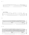
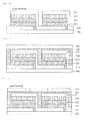
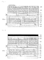
- FIG. 9 to FIG. 24 are sectional views of a stack structure of modules illustrating a method of manufacturing the thin-film solar cell in response to process steps according to the preferred embodiment of the present invention.
- a manufacture method comprises the steps of: forming a first solar cell layer; forming a second solar cell layer formed of semiconductor materials having band gap energy which are different from the first solar cell layer; and electrically connecting the first solar cell layer with the second solar cell layer in parallel, and further comprises processes of providing a transparent conductive layer at an upper part and a lower part of each solar cell layer and forming a back-side electrode layer at the upper part of the second solar cell layer.
- first solar cell layer and the second solar cell layer may be consecutively stacked up and down, a process for forming insulating layers between both the solar cells is added.
- a pair of electrode connectors 360a, 360b may be separately connected as the above example embodiment, and simultaneously connected after all process is finished.
- FIG. 25 is a top plan view illustrating the thin-film solar cell module according to the preferred embodiment of the present invention.
- the upper electrode connection site is directly opposite to the lower electrode connection site and it is possible to connect the upper and lower electrodes at any site within the unit cells of the solar cell layer.
- the present invention may be used for providing a solar cell having a thin-film solar cell structure, which is capable of increasing a photoelectric conversion efficiency and a stable reliability and may be utilized for a method of manufacturing the solar cell, which is capable of producing a large area solar cell through a relatively simple process and at low fabrication costs.
- the present invention provides a structure of the solar cell and a method of manufacturing the same, which are capable of having a high photoelectric conversion efficiency and producing solar cells having large area at low-costs, and accordingly, will contribute to protecting earth's environment by providing clean energy resources for the next generation and create great economic benefit by its application to public facilities, private facilities, munitions facilities and other various fields.
Landscapes
- Photovoltaic Devices (AREA)
Applications Claiming Priority (1)
| Application Number | Priority Date | Filing Date | Title |
|---|---|---|---|
| KR1020070019097A KR20080079058A (ko) | 2007-02-26 | 2007-02-26 | 박막형 태양전지 모듈과 그의 제조방법 |
Publications (2)
| Publication Number | Publication Date |
|---|---|
| EP1962331A2 true EP1962331A2 (de) | 2008-08-27 |
| EP1962331A3 EP1962331A3 (de) | 2012-09-26 |
Family
ID=39537922
Family Applications (1)
| Application Number | Title | Priority Date | Filing Date |
|---|---|---|---|
| EP08101896A Withdrawn EP1962331A3 (de) | 2007-02-26 | 2008-02-22 | Dünnschichtige Solarzelle und Verfahren zu ihrer Herstellung |
Country Status (4)
| Country | Link |
|---|---|
| US (1) | US7863515B2 (de) |
| EP (1) | EP1962331A3 (de) |
| JP (1) | JP2008211217A (de) |
| KR (1) | KR20080079058A (de) |
Cited By (8)
| Publication number | Priority date | Publication date | Assignee | Title |
|---|---|---|---|---|
| DE102008049374A1 (de) | 2008-09-27 | 2010-04-01 | JODLAUK, Jörg | Halbleiterfaserstrukturen als Energieerzeuger |
| WO2010024636A3 (en) * | 2008-09-01 | 2010-06-24 | Lg Electronics Inc. | Thin-film type solar cell and method for manufacturing the same |
| WO2010080672A2 (en) | 2009-01-06 | 2010-07-15 | Sunlight Photonics Inc. | Multi-junction pv module |
| EP2375455A1 (de) * | 2010-04-09 | 2011-10-12 | S.O.I.Tec Silicon on Insulator Technologies | Spannungsangepasste Multiverbindungssolarzelle |
| EP2851965A3 (de) * | 2013-09-24 | 2015-06-03 | Kabushiki Kaisha Toshiba | Solarzellen mit mehreren Anschlüssen |
| EP3213351A1 (de) * | 2014-10-28 | 2017-09-06 | Sol Voltaics AB | Doppelschichtiges fotovoltaikmodul |
| EP2421026A4 (de) * | 2009-04-15 | 2017-11-29 | Huilong Zhu | Substratstruktur zur herstellung einer halbleitervorrichtung und herstellungsverfahren dafür |
| CN108767023A (zh) * | 2018-06-26 | 2018-11-06 | 米亚索乐装备集成(福建)有限公司 | 栅电极、太阳能电池及其制备方法 |
Families Citing this family (54)
| Publication number | Priority date | Publication date | Assignee | Title |
|---|---|---|---|---|
| JP5069791B2 (ja) * | 2008-05-22 | 2012-11-07 | 株式会社カネカ | 薄膜光電変換装置とその製造方法 |
| US8748799B2 (en) | 2010-12-14 | 2014-06-10 | Zena Technologies, Inc. | Full color single pixel including doublet or quadruplet si nanowires for image sensors |
| US9082673B2 (en) | 2009-10-05 | 2015-07-14 | Zena Technologies, Inc. | Passivated upstanding nanostructures and methods of making the same |
| US8229255B2 (en) | 2008-09-04 | 2012-07-24 | Zena Technologies, Inc. | Optical waveguides in image sensors |
| US9299866B2 (en) | 2010-12-30 | 2016-03-29 | Zena Technologies, Inc. | Nanowire array based solar energy harvesting device |
| US9343490B2 (en) | 2013-08-09 | 2016-05-17 | Zena Technologies, Inc. | Nanowire structured color filter arrays and fabrication method of the same |
| US9000353B2 (en) | 2010-06-22 | 2015-04-07 | President And Fellows Of Harvard College | Light absorption and filtering properties of vertically oriented semiconductor nano wires |
| US8866065B2 (en) | 2010-12-13 | 2014-10-21 | Zena Technologies, Inc. | Nanowire arrays comprising fluorescent nanowires |
| US9515218B2 (en) | 2008-09-04 | 2016-12-06 | Zena Technologies, Inc. | Vertical pillar structured photovoltaic devices with mirrors and optical claddings |
| US8274039B2 (en) | 2008-11-13 | 2012-09-25 | Zena Technologies, Inc. | Vertical waveguides with various functionality on integrated circuits |
| US8299472B2 (en) | 2009-12-08 | 2012-10-30 | Young-June Yu | Active pixel sensor with nanowire structured photodetectors |
| US8546742B2 (en) | 2009-06-04 | 2013-10-01 | Zena Technologies, Inc. | Array of nanowires in a single cavity with anti-reflective coating on substrate |
| US9406709B2 (en) | 2010-06-22 | 2016-08-02 | President And Fellows Of Harvard College | Methods for fabricating and using nanowires |
| US9478685B2 (en) | 2014-06-23 | 2016-10-25 | Zena Technologies, Inc. | Vertical pillar structured infrared detector and fabrication method for the same |
| US8835831B2 (en) | 2010-06-22 | 2014-09-16 | Zena Technologies, Inc. | Polarized light detecting device and fabrication methods of the same |
| US8735797B2 (en) | 2009-12-08 | 2014-05-27 | Zena Technologies, Inc. | Nanowire photo-detector grown on a back-side illuminated image sensor |
| US20140150857A1 (en) * | 2012-12-04 | 2014-06-05 | Zena Technologies, Inc. | Multi-junction multi-tab photovoltaic devices |
| JP2010278405A (ja) * | 2009-06-01 | 2010-12-09 | Smart Solar International Inc | 太陽光発電システム及び太陽光発電装置 |
| CN102460721B (zh) * | 2009-06-05 | 2015-07-01 | 株式会社半导体能源研究所 | 光电转换装置及其制造方法 |
| WO2010140539A1 (en) * | 2009-06-05 | 2010-12-09 | Semiconductor Energy Laboratory Co., Ltd. | Photoelectric conversion device and method for manufacturing the same |
| KR101732397B1 (ko) * | 2009-06-05 | 2017-05-04 | 가부시키가이샤 한도오따이 에네루기 켄큐쇼 | 광전 변환 장치 및 그의 제작 방법 |
| US8647995B2 (en) * | 2009-07-24 | 2014-02-11 | Corsam Technologies Llc | Fusion formable silica and sodium containing glasses |
| KR101026362B1 (ko) * | 2009-09-25 | 2011-04-05 | 한국과학기술원 | 실리콘 태양전지 |
| JP2013506995A (ja) * | 2009-10-01 | 2013-02-28 | エルジー イノテック カンパニー リミテッド | 太陽光発電装置及びその製造方法 |
| KR101067295B1 (ko) * | 2009-10-07 | 2011-09-26 | 한국과학기술원 | 박막 태양전지 및 그의 제조방법 |
| US20110120534A1 (en) * | 2009-11-20 | 2011-05-26 | Auria Solar Co., Ltd. | Thin film solar cell and manufacturing method thereof |
| TW201123511A (en) * | 2009-12-31 | 2011-07-01 | Auria Solar Co Ltd | Method for fabricating thin film solar cell and thin film solar cell |
| US8563351B2 (en) * | 2010-06-25 | 2013-10-22 | Taiwan Semiconductor Manufacturing Co., Ltd. | Method for manufacturing photovoltaic device |
| CN102412323A (zh) * | 2010-09-20 | 2012-04-11 | 亚洲太阳科技有限公司 | 低成本改良式薄膜太阳能电池封装材料 |
| CN102437231A (zh) * | 2010-09-29 | 2012-05-02 | 亚洲太阳科技有限公司 | 低成本改良式薄膜太阳能电池设备设计准则 |
| US20140202515A1 (en) * | 2011-06-16 | 2014-07-24 | 3M Innovative Properties Company | Booster films for solar photovoltaic systems |
| EP2555243A1 (de) * | 2011-08-03 | 2013-02-06 | STMicroelectronics S.r.l. | Dünnschicht-Solarzellenmodul mit hintereinander geschalteten Zellen, die mittels Lithografie auf einem flexiblen Substrat geformt werden |
| CN102956650A (zh) * | 2011-08-26 | 2013-03-06 | 刘莹 | 一种新型叠层薄膜太阳能电池 |
| CN103107247A (zh) * | 2011-11-09 | 2013-05-15 | 海立尔股份有限公司 | Led芯片的制造方法及其结构 |
| KR101289832B1 (ko) * | 2012-03-06 | 2013-07-30 | 한주원 | 태양전지 및 그 제조방법 |
| TW201347206A (zh) * | 2012-05-10 | 2013-11-16 | Gcsol Tech Co Ltd | 層疊型太陽能電池結構 |
| US9701567B2 (en) | 2013-04-29 | 2017-07-11 | Corning Incorporated | Photovoltaic module package |
| US9093599B2 (en) | 2013-07-26 | 2015-07-28 | First Solar, Inc. | Vapor deposition apparatus for continuous deposition of multiple thin film layers on a substrate |
| WO2015151422A1 (ja) * | 2014-03-31 | 2015-10-08 | 国立研究開発法人科学技術振興機構 | 太陽電池および太陽電池の製造方法 |
| CN104009117B (zh) * | 2014-05-15 | 2017-02-01 | 浙江正泰太阳能科技有限公司 | 一种柔性薄膜太阳能电池及其制备方法 |
| JP6338990B2 (ja) * | 2014-09-19 | 2018-06-06 | 株式会社東芝 | 多接合型太陽電池 |
| WO2016208034A1 (ja) * | 2015-06-25 | 2016-12-29 | 株式会社 東芝 | 太陽電池モジュール |
| GB2548361B (en) | 2016-03-15 | 2020-12-02 | Dyson Technology Ltd | Method of fabricating an energy storage device |
| GB2566472B (en) | 2017-09-14 | 2020-03-04 | Dyson Technology Ltd | Magnesium salts |
| GB2566473B (en) | 2017-09-14 | 2020-03-04 | Dyson Technology Ltd | Magnesium salts |
| GB2569388B (en) | 2017-12-18 | 2022-02-02 | Dyson Technology Ltd | Compound |
| GB2569390A (en) | 2017-12-18 | 2019-06-19 | Dyson Technology Ltd | Compound |
| GB2569387B (en) | 2017-12-18 | 2022-02-02 | Dyson Technology Ltd | Electrode |
| GB2569392B (en) | 2017-12-18 | 2022-01-26 | Dyson Technology Ltd | Use of aluminium in a cathode material |
| CN108155293A (zh) * | 2017-12-30 | 2018-06-12 | 凯盛光伏材料有限公司 | 一种铜铟镓硒钙钛矿叠层太阳能电池及其制备方法 |
| CN113785407A (zh) * | 2019-06-07 | 2021-12-10 | 松下知识产权经营株式会社 | 四端子串联太阳能电池 |
| KR102624394B1 (ko) * | 2020-11-27 | 2024-01-15 | 한국과학기술연구원 | 탠덤 태양전지 모듈 |
| JP7633622B2 (ja) * | 2021-01-26 | 2025-02-20 | 西松建設株式会社 | 光電変換素子、発電装置 |
| CN113594288B (zh) * | 2021-09-28 | 2021-12-21 | 中国华能集团清洁能源技术研究院有限公司 | 内串联式异质结电池及其制作方法 |
Family Cites Families (10)
| Publication number | Priority date | Publication date | Assignee | Title |
|---|---|---|---|---|
| US4316049A (en) * | 1979-08-28 | 1982-02-16 | Rca Corporation | High voltage series connected tandem junction solar battery |
| JPS59161081A (ja) * | 1983-03-03 | 1984-09-11 | Fuji Electric Corp Res & Dev Ltd | 薄膜太陽電池 |
| JPS6030163A (ja) * | 1983-07-28 | 1985-02-15 | Fuji Electric Corp Res & Dev Ltd | 薄膜太陽電池モジユ−ル |
| JPS60123073A (ja) * | 1983-12-08 | 1985-07-01 | Fuji Electric Corp Res & Dev Ltd | 薄膜太陽電池 |
| JPS6175567A (ja) * | 1984-09-20 | 1986-04-17 | Sanyo Electric Co Ltd | 光起電力装置 |
| JPS62221167A (ja) * | 1986-03-24 | 1987-09-29 | Seiji Wakamatsu | 多層型薄膜太陽電池 |
| DE3727823A1 (de) * | 1987-08-20 | 1989-03-02 | Siemens Ag | Tandem-solarmodul |
| US5071490A (en) * | 1988-03-18 | 1991-12-10 | Sharp Kabushiki Kaisha | Tandem stacked amorphous solar cell device |
| US7812249B2 (en) * | 2003-04-14 | 2010-10-12 | The Boeing Company | Multijunction photovoltaic cell grown on high-miscut-angle substrate |
| US20050150542A1 (en) * | 2004-01-13 | 2005-07-14 | Arun Madan | Stable Three-Terminal and Four-Terminal Solar Cells and Solar Cell Panels Using Thin-Film Silicon Technology |
-
2007
- 2007-02-26 KR KR1020070019097A patent/KR20080079058A/ko not_active Ceased
-
2008
- 2008-02-22 US US12/035,927 patent/US7863515B2/en not_active Expired - Fee Related
- 2008-02-22 EP EP08101896A patent/EP1962331A3/de not_active Withdrawn
- 2008-02-25 JP JP2008042714A patent/JP2008211217A/ja active Pending
Cited By (17)
| Publication number | Priority date | Publication date | Assignee | Title |
|---|---|---|---|---|
| KR101144808B1 (ko) | 2008-09-01 | 2012-05-11 | 엘지전자 주식회사 | 박막형 태양전지 제조방법 및 이를 이용한 박막형 태양전지 |
| WO2010024636A3 (en) * | 2008-09-01 | 2010-06-24 | Lg Electronics Inc. | Thin-film type solar cell and method for manufacturing the same |
| EP2573813A1 (de) * | 2008-09-01 | 2013-03-27 | LG Electronics Inc. | Herstellungsverfahren mit reduzierter Anzahl von Strukturierungsschritten für eine Dünnschichtsolarzelle mit serienverschalteten Basiszellen und entsprechende Vorrichtung |
| DE102008049374A1 (de) | 2008-09-27 | 2010-04-01 | JODLAUK, Jörg | Halbleiterfaserstrukturen als Energieerzeuger |
| US8835748B2 (en) | 2009-01-06 | 2014-09-16 | Sunlight Photonics Inc. | Multi-junction PV module |
| EP2386122A4 (de) * | 2009-01-06 | 2013-02-20 | Sunlight Photonics Inc | Mehrfachübergangs-pv-modul |
| WO2010080672A2 (en) | 2009-01-06 | 2010-07-15 | Sunlight Photonics Inc. | Multi-junction pv module |
| US9087948B1 (en) | 2009-01-06 | 2015-07-21 | Sunlight Photonics Inc. | Manufacturing method of multi-junction PV modules |
| EP2421026A4 (de) * | 2009-04-15 | 2017-11-29 | Huilong Zhu | Substratstruktur zur herstellung einer halbleitervorrichtung und herstellungsverfahren dafür |
| WO2011124321A3 (en) * | 2010-04-09 | 2012-05-31 | Soitec | Voltage matched multijunction solar cell |
| EP2375455A1 (de) * | 2010-04-09 | 2011-10-12 | S.O.I.Tec Silicon on Insulator Technologies | Spannungsangepasste Multiverbindungssolarzelle |
| US10714644B2 (en) | 2010-04-09 | 2020-07-14 | Saint-Augustin Canada Electric Inc. | Voltage matched multijunction solar cell |
| US11482633B2 (en) | 2010-04-09 | 2022-10-25 | Saint-Augustin Canada Electric Inc. | Voltage matched multijunction solar cell |
| EP2851965A3 (de) * | 2013-09-24 | 2015-06-03 | Kabushiki Kaisha Toshiba | Solarzellen mit mehreren Anschlüssen |
| US11398577B2 (en) | 2013-09-24 | 2022-07-26 | Kabushiki Kaisha Toshiba | Multi-junction solar cell |
| EP3213351A1 (de) * | 2014-10-28 | 2017-09-06 | Sol Voltaics AB | Doppelschichtiges fotovoltaikmodul |
| CN108767023A (zh) * | 2018-06-26 | 2018-11-06 | 米亚索乐装备集成(福建)有限公司 | 栅电极、太阳能电池及其制备方法 |
Also Published As
| Publication number | Publication date |
|---|---|
| JP2008211217A (ja) | 2008-09-11 |
| US7863515B2 (en) | 2011-01-04 |
| US20080264478A1 (en) | 2008-10-30 |
| KR20080079058A (ko) | 2008-08-29 |
| EP1962331A3 (de) | 2012-09-26 |
Similar Documents
| Publication | Publication Date | Title |
|---|---|---|
| US7863515B2 (en) | Thin-film solar cell and method of manufacturing the same | |
| US9087948B1 (en) | Manufacturing method of multi-junction PV modules | |
| US9960302B1 (en) | Cascaded photovoltaic structures with interdigitated back contacts | |
| EP3170209B1 (de) | Solarzelle mit verfingertem rückseitenkontakt | |
| US9287431B2 (en) | Superstrate sub-cell voltage-matched multijunction solar cells | |
| US9293619B2 (en) | Smart photovoltaic cells and modules | |
| AU2013331304B2 (en) | Systems and methods for monolithically integrated bypass switches in photovoltaic solar cells and modules | |
| US9147783B2 (en) | Apparatus and method for hybrid photovoltaic device having multiple, stacked, heterogeneous, semiconductor junctions | |
| US20090242018A1 (en) | Thin-film solar cell and fabrication method thereof | |
| US20150340528A1 (en) | Monolithic tandem voltage-matched multijuntion solar cells | |
| US20060231130A1 (en) | Solar cell with feedthrough via | |
| US11996491B2 (en) | Solar cell module | |
| CN107112376A (zh) | 双层光伏设备 | |
| CN106298998A (zh) | 一种叠层并联的太阳能电池组件、制作方法及装置 | |
| Mil'Shtein et al. | Cascaded heterostructured a-Si/c-Si Solar Cell with increased current production | |
| CN219591399U (zh) | 叠层太阳能电池组件 | |
| US9040342B2 (en) | Photovoltaic cell and manufacturing method thereof | |
| US20120298169A1 (en) | Multi-junction Photovoltaic Cells | |
| HK1236677A1 (en) | Dual layer photovoltaic device |
Legal Events
| Date | Code | Title | Description |
|---|---|---|---|
| PUAI | Public reference made under article 153(3) epc to a published international application that has entered the european phase |
Free format text: ORIGINAL CODE: 0009012 |
|
| 17P | Request for examination filed |
Effective date: 20080222 |
|
| AK | Designated contracting states |
Kind code of ref document: A2 Designated state(s): AT BE BG CH CY CZ DE DK EE ES FI FR GB GR HR HU IE IS IT LI LT LU LV MC MT NL NO PL PT RO SE SI SK TR |
|
| AX | Request for extension of the european patent |
Extension state: AL BA MK RS |
|
| PUAL | Search report despatched |
Free format text: ORIGINAL CODE: 0009013 |
|
| AK | Designated contracting states |
Kind code of ref document: A3 Designated state(s): AT BE BG CH CY CZ DE DK EE ES FI FR GB GR HR HU IE IS IT LI LT LU LV MC MT NL NO PL PT RO SE SI SK TR |
|
| AX | Request for extension of the european patent |
Extension state: AL BA MK RS |
|
| RIC1 | Information provided on ipc code assigned before grant |
Ipc: H01L 25/04 20060101ALI20120823BHEP Ipc: H01L 27/142 20060101ALI20120823BHEP Ipc: H01L 31/0392 20060101ALI20120823BHEP Ipc: H01L 21/268 20060101AFI20120823BHEP Ipc: H01L 31/075 20120101ALI20120823BHEP |
|
| AKY | No designation fees paid | ||
| REG | Reference to a national code |
Ref country code: DE Ref legal event code: R108 Effective date: 20130529 |
|
| STAA | Information on the status of an ep patent application or granted ep patent |
Free format text: STATUS: THE APPLICATION IS DEEMED TO BE WITHDRAWN |
|
| 18D | Application deemed to be withdrawn |
Effective date: 20130327 |