EP1962679B1 - Procedes de fabrication de micro-aiguilles et applications de celles-ci - Google Patents
Procedes de fabrication de micro-aiguilles et applications de celles-ci Download PDFInfo
- Publication number
- EP1962679B1 EP1962679B1 EP06824640A EP06824640A EP1962679B1 EP 1962679 B1 EP1962679 B1 EP 1962679B1 EP 06824640 A EP06824640 A EP 06824640A EP 06824640 A EP06824640 A EP 06824640A EP 1962679 B1 EP1962679 B1 EP 1962679B1
- Authority
- EP
- European Patent Office
- Prior art keywords
- substrate
- mask
- needles
- wafer
- etch
- Prior art date
- Legal status (The legal status is an assumption and is not a legal conclusion. Google has not performed a legal analysis and makes no representation as to the accuracy of the status listed.)
- Active
Links
Images













Classifications
-
- A—HUMAN NECESSITIES
- A61—MEDICAL OR VETERINARY SCIENCE; HYGIENE
- A61M—DEVICES FOR INTRODUCING MEDIA INTO, OR ONTO, THE BODY; DEVICES FOR TRANSDUCING BODY MEDIA OR FOR TAKING MEDIA FROM THE BODY; DEVICES FOR PRODUCING OR ENDING SLEEP OR STUPOR
- A61M37/00—Other apparatus for introducing media into the body; Percutany, i.e. introducing medicines into the body by diffusion through the skin
- A61M37/0015—Other apparatus for introducing media into the body; Percutany, i.e. introducing medicines into the body by diffusion through the skin by using microneedles
-
- A—HUMAN NECESSITIES
- A61—MEDICAL OR VETERINARY SCIENCE; HYGIENE
- A61B—DIAGNOSIS; SURGERY; IDENTIFICATION
- A61B5/00—Measuring for diagnostic purposes; Identification of persons
- A61B5/15—Devices for taking samples of blood
- A61B5/150007—Details
- A61B5/150015—Source of blood
- A61B5/150022—Source of blood for capillary blood or interstitial fluid
-
- A—HUMAN NECESSITIES
- A61—MEDICAL OR VETERINARY SCIENCE; HYGIENE
- A61B—DIAGNOSIS; SURGERY; IDENTIFICATION
- A61B5/00—Measuring for diagnostic purposes; Identification of persons
- A61B5/15—Devices for taking samples of blood
- A61B5/150007—Details
- A61B5/150206—Construction or design features not otherwise provided for; manufacturing or production; packages; sterilisation of piercing element, piercing device or sampling device
- A61B5/150274—Manufacture or production processes or steps for blood sampling devices
- A61B5/150282—Manufacture or production processes or steps for blood sampling devices for piercing elements, e.g. blade, lancet, canula, needle
-
- A—HUMAN NECESSITIES
- A61—MEDICAL OR VETERINARY SCIENCE; HYGIENE
- A61B—DIAGNOSIS; SURGERY; IDENTIFICATION
- A61B5/00—Measuring for diagnostic purposes; Identification of persons
- A61B5/15—Devices for taking samples of blood
- A61B5/150977—Arrays of piercing elements for simultaneous piercing
- A61B5/150984—Microneedles or microblades
-
- A—HUMAN NECESSITIES
- A61—MEDICAL OR VETERINARY SCIENCE; HYGIENE
- A61N—ELECTROTHERAPY; MAGNETOTHERAPY; RADIATION THERAPY; ULTRASOUND THERAPY
- A61N1/00—Electrotherapy; Circuits therefor
- A61N1/02—Details
- A61N1/04—Electrodes
- A61N1/05—Electrodes for implantation or insertion into the body, e.g. heart electrode
- A61N1/0502—Skin piercing electrodes
-
- A—HUMAN NECESSITIES
- A61—MEDICAL OR VETERINARY SCIENCE; HYGIENE
- A61N—ELECTROTHERAPY; MAGNETOTHERAPY; RADIATION THERAPY; ULTRASOUND THERAPY
- A61N1/00—Electrotherapy; Circuits therefor
- A61N1/02—Details
- A61N1/04—Electrodes
- A61N1/05—Electrodes for implantation or insertion into the body, e.g. heart electrode
- A61N1/0551—Spinal or peripheral nerve electrodes
-
- A—HUMAN NECESSITIES
- A61—MEDICAL OR VETERINARY SCIENCE; HYGIENE
- A61B—DIAGNOSIS; SURGERY; IDENTIFICATION
- A61B5/00—Measuring for diagnostic purposes; Identification of persons
- A61B5/05—Detecting, measuring or recording for diagnosis by means of electric currents or magnetic fields; Measuring using microwaves or radio waves
- A61B5/053—Measuring electrical impedance or conductance of a portion of the body
-
- A—HUMAN NECESSITIES
- A61—MEDICAL OR VETERINARY SCIENCE; HYGIENE
- A61M—DEVICES FOR INTRODUCING MEDIA INTO, OR ONTO, THE BODY; DEVICES FOR TRANSDUCING BODY MEDIA OR FOR TAKING MEDIA FROM THE BODY; DEVICES FOR PRODUCING OR ENDING SLEEP OR STUPOR
- A61M37/00—Other apparatus for introducing media into the body; Percutany, i.e. introducing medicines into the body by diffusion through the skin
- A61M37/0015—Other apparatus for introducing media into the body; Percutany, i.e. introducing medicines into the body by diffusion through the skin by using microneedles
- A61M2037/003—Other apparatus for introducing media into the body; Percutany, i.e. introducing medicines into the body by diffusion through the skin by using microneedles having a lumen
-
- A—HUMAN NECESSITIES
- A61—MEDICAL OR VETERINARY SCIENCE; HYGIENE
- A61M—DEVICES FOR INTRODUCING MEDIA INTO, OR ONTO, THE BODY; DEVICES FOR TRANSDUCING BODY MEDIA OR FOR TAKING MEDIA FROM THE BODY; DEVICES FOR PRODUCING OR ENDING SLEEP OR STUPOR
- A61M37/00—Other apparatus for introducing media into the body; Percutany, i.e. introducing medicines into the body by diffusion through the skin
- A61M37/0015—Other apparatus for introducing media into the body; Percutany, i.e. introducing medicines into the body by diffusion through the skin by using microneedles
- A61M2037/0046—Solid microneedles
-
- A—HUMAN NECESSITIES
- A61—MEDICAL OR VETERINARY SCIENCE; HYGIENE
- A61M—DEVICES FOR INTRODUCING MEDIA INTO, OR ONTO, THE BODY; DEVICES FOR TRANSDUCING BODY MEDIA OR FOR TAKING MEDIA FROM THE BODY; DEVICES FOR PRODUCING OR ENDING SLEEP OR STUPOR
- A61M37/00—Other apparatus for introducing media into the body; Percutany, i.e. introducing medicines into the body by diffusion through the skin
- A61M37/0015—Other apparatus for introducing media into the body; Percutany, i.e. introducing medicines into the body by diffusion through the skin by using microneedles
- A61M2037/0053—Methods for producing microneedles
-
- H—ELECTRICITY
- H10—SEMICONDUCTOR DEVICES; ELECTRIC SOLID-STATE DEVICES NOT OTHERWISE PROVIDED FOR
- H10W—GENERIC PACKAGES, INTERCONNECTIONS, CONNECTORS OR OTHER CONSTRUCTIONAL DETAILS OF DEVICES COVERED BY CLASS H10
- H10W72/00—Interconnections or connectors in packages
- H10W72/01—Manufacture or treatment
- H10W72/015—Manufacture or treatment of bond wires
- H10W72/01515—Forming coatings
-
- H—ELECTRICITY
- H10—SEMICONDUCTOR DEVICES; ELECTRIC SOLID-STATE DEVICES NOT OTHERWISE PROVIDED FOR
- H10W—GENERIC PACKAGES, INTERCONNECTIONS, CONNECTORS OR OTHER CONSTRUCTIONAL DETAILS OF DEVICES COVERED BY CLASS H10
- H10W72/00—Interconnections or connectors in packages
- H10W72/071—Connecting or disconnecting
- H10W72/075—Connecting or disconnecting of bond wires
Definitions
- the present invention relates to methods for making needles in the micrometer scale.
- it relates to the manufacture of needles having a tip resembling a cannula type of tip, i.e. with an inclined tip portion.
- Micro-sized needles i.e. needles having diameters and lengths in the micrometer range, find great utility i.a. in many medical applications.
- injection of liquid such as drugs of various kinds, vaccines etc. through the skin is often performed.
- ordinary syringes are used for the administration it can sometimes cause pain or discomfort to a patient.
- Micro-needles can be used in such applications to reduce the pain experienced by the patient.
- arrays of hollow micro-needles provided on a patch that is applied to the skin and through which medicaments are administered will reduce the pain and discomfort substantially.
- US published patent application 2004/0054393 discloses a medical electrode for obtaining biopotentials from the skin of a subject or electrically stimulating the subject's skin and deeper tissue layers.
- the electrode has a carrier base member from which project a plurality of spikes arranged in an array on one surface of the base member.
- the spikes are sufficiently long to penetrate through the stratum corneum into the stratum germinativum of the subject's skin.
- the spikes may be formed by a deep reactive ion etching process on a silicon wafer forming the base member.
- a fluid container may be formed on another surface of the skin for providing a drug to the surface of the skin through holes in the base member. The action of the spikes on the skin enhances administration of the drug.
- the needles have what is referred to as “rocket tips", and are made by an isotropic-anisotropic-isotropic etch sequence.
- US-5,855,801 discloses a method of fabricating a microstructure.
- the method includes providing a substrate for forming an interface region and an elongated portion extending away from the interface region.
- a patterned, nonplanar etchable structure is formed on one side of the elongated portion of the substrate.
- An unetchable membrane layer is deposited atop the etchable structure.
- At least one etching hole is formed in the membrane layer.
- the etchable structure is etched by placing an etchant into the etching hole to form a cavity underneath the membrane layer, thereby producing a shaft.
- WO 2003/015860 discloses a method of making a needle having side openings. It comprises providing a mask on the front side of an etchable wafer such that the vertical projection of said mask at least partially covers the extension of a hole made in the back side. Said mask is isotropically underetched to remove wafer material. An anisotropic etch forms a protruding structure. Optionally a second isotropic etch on said protruding structure exposes the blind hole. Optionally a final anisotropic etch extends the needle without forming side openings. The position and extension of the mask relative the position and dimension of the hole is such that said side openings form during either said anisotropic etc or said second isotropic etch.
- US-6,334,856 discloses a method for making a microneedle. It includes forming a micromold having sidewalls which define the outer surface of the microneedle, electroplating the sidewalls to form the hollow microneedle, and then removing the micromold from the microneedle.
- US-6,533,949 discloses a method for processing a wafer to form a plurality of hollow microneedles projecting from a substrate includes forming, by use of a dry etching process, a number of groups of recessed features, each including at least one slot deployed to form an open shape having an included area and at least one hole located within the included area. The internal surfaces of the holes and the slots are then coated with a protective layer. An anisotropic wet etching process is then performed in such a manner as to remove material from outside the included areas while leaving a projecting feature within each of the included areas. The protective layer is then removed to reveal the microneedles.
- a problem with prior art devices having micro-needles used in the medical field is to achieve appropriate penetration of the outer skin layer, the stratum corneum. In particular it is important to avoid deep penetration so as to intervene with the nerves.
- an object of the present invention is to provide new methods for making devices having micro-needles wherein the problems of the prior art devices, such as bad or unsatisfactory penetration of the stratum corneum, are eliminated or reduced.
- the present invention provides an improved method of making micro structures protruding from a surface, such as micro needles, and having an obliquely cut tip, resembling a tip on a cannula.
- the method according to the invention in its first aspect is defined in claim 1, and comprises making vertically protruding elements on a substrate, said elements having a tip comprising at least one inclined surface and an elongated body portion extending between said substrate and said tip, the method comprising, an anisotropic, crystal plane dependent etch forming said inclined surface(s), and an anisotropic, non crystal plane dependent etch forming said elongated body portion, and selectively patterning the inclined surfaces resulting in a pattern defining a base geometry for the protuding element to be made.
- the method comprises providing an etchable substrate having a first side and a second side at least one side of which is single crystalline, patterning said substrate on said single crystalline side to form an etching mask so as to expose selected areas thereof, performing an anisotropic etching process through said mask to expose a selected crystal plane of said single crystalline substrate to provide at least one inclined surface, selectively patterning said inclined surface(s) resulting in a pattern defining a base geometry for the protruding element to be made, performing an anisotropic etching procedure to remove material essentially in the vertical direction only so as to leave vertically protruding elements according to said pattern.
- the method further comprises aligning the pattern to selected crystal orientations of said substrate.
- the patterning step further comprises using, for the mask, a material that resists the etching that provides the inclined surface.
- the mask preferably comprises areas having at least one edge aligned with the crystal orientation of the wafer, i.e. parallel with at least one crystal plane.
- the mask comprises discrete areas of mask material for defining a protruding element having inclined surfaces.
- the mask can comprise open areas exposing the wafer for defining depressions having inclined surfaces.
- the step of patterning the inclined surface(s) may comprise providing a uniformly thick masking layer by spraying or spinning.
- the etching to provide the inclined surface(s) can be performed by using a wet etch, preferably selected from aqueous KOH, NaOH, TMAH, EDP, most preferably the etch is a KOH etch.
- the etching to provide the vertically protruding elements is performed by using a DRIE etch.
- the substrate is a SOI wafer.
- the finished wafer should be at least partially metallized to provide connection between the first and the second side of the wafer.
- the needles can be made both as solid and as hollow needles, the latter form being suitable for delivering fluids, e.g. drugs to a patient through the skin.
- the former i.e. solid needles can be used for electrical applications, e.g. impedance and resistitvity measurements, measurements of biopotentials (EEG, EKG, EMG etc.).
- Solid needles can also be used for applications such as emitters.
- Solid needles can also be used for pretreatment of the skin instead of using sand paper, which is common today, for removing the outer skin layer so as to enable direct uptake of a drug applied to the skin.
- An advantage of the method and the devices obtained therewith according to the first aspect of the present invention over prior art methods is i.a. that an improved penetration of the outer skin layer is achieved.
- the new method enables manufacturing in high yields.
- the present invention preferably provides an improved method of making micro needles having a polygonal, such as square, rectangular etc., base and a pointed tip, the needles being either solid or hollow.
- An advantage of the method and devices obtained therewith over prior art methods is that improved cutting in the tissue is achieved by virtue of the polygonal shape forming edges capable of cutting through tissue, thereby further improving the penetration performance of the needles.
- the present invention preferably provides a method of making a device for electrical measurements, e.g. impedance measurements.
- the method enables the manufacture isolated groups or arrays of needles integrated on one chip, which provides for well defined distances between needles, and the groups/arrays of needles.
- manufacture of electrodes having single groups or arrays of micro-needles, e.g. for ECG applications, is also enabled with this method.
- the method of making devices for electrical measurements comprises the steps of providing a substrate having a first side and a second side; making the micro-electrodes on the substrate; at least partially metallizing the substrate with said micro-electrodes to provide electrical connection between the first and second sides of said substrate.
- a method of making rotationally symmetric vertically protruding elements on a substrate comprising the following steps of providing an etchable substrate having a first side and a second side at least one side of which is single crystalline, patterning said substrate on said single crystalline side to form an etching mask so as to expose selected areas of the substrate, performing an anisotropic etching process through said mask to expose one or more selected crystal planes of said single crystalline substrate to provide a plurality of inclined surfaces; performing an anisotropic etching procedure to remove material essentially in the vertical direction only so as to leave vertically protruding elements according to said pattern.
- the invention further preferably provides a method of making devices for electrical measurements, each device comprising a plurality of micro-electrodes in the form of micro-needles protruding vertically from a substrate, the method comprising the steps of: providing a substrate having a first side and a second side; making the micro-electrodes on the substrate; at least partially metallizing the substrate with said micro-electrodes to provide electrical connection between the first and second sides of said substrate, and further comprising electrically insulating groups of micro-electrodes from each other.
- the method comprises making the micro-needles by a process comprising: patterning said substrate, which has a first side which is single crystalline and a second side, on said first single crystalline side to form a mask so as to expose selected areas of the substrate, whereby the mask defines a device, said device comprising at least two groups of micro-electrodes protruding from said substrate; performing an anisotropic etching process through said mask to expose a selected crystal plane of said single crystalline substrate to provide at least one inclined surface; selectively patterning said inclined surface(s) resulting in a pattern defining a base geometry for the protruding micro-electrodes to be made; performing an anisotropic etching procedure to remove material essentially in the vertical direction only so as to leave vertically protruding micro-electrodes according to said pattern.
- the step of electrically insulating the micro-electrodes suitably comprises attaching the wafer to an insulating substrate, such as glass, and removing wafer material between said groups at least down to said insulating substrate.
- the electrical insulation between groups of micro-electrodes is preferably achieved by using a SOI wafer as the starting substrate and removing material from the device layer of said SOI wafer at least down to the insulating layer thereof.
- part of the insulator layer of the SOI wafer is suitably removed to expose the silicon underneath the insulator layer, and wherein the metallization is limited to cover the exposed silicon, the needles and the area between the micro-electrodes and the silicon so as to create an electrical connection between the micro-electrodes and the silicon.
- the insulator is suitably removed by making a recess through the layer and down to the silicon underneath the insulator layer. Removing can be made by any of sawing, laser cutting, drilling, blasting, or alternatively by etching a recess through the layer and down to the silicon underneath the insulator layer.
- the metallization can be made through a shadow mask exposing only those areas to be metallised, or by a lift-off process, wherein before metallization, a resist is applied and patterned to expose only those areas where insulation is to be provided between groups of micro-electrodes, then the entire wafer is metallized, and finally the resist is removed whereby the metallization on top of the resist is removed.
- the entire wafer can be metallized; an insulator can be deposited only on those areas between micro-electrodes that are to be electrically insulated from each other; and recesses can be made through the metallization down through the SOI insulator layer and down to the silicon beneath, such that groups of micro-electrodes become electrically insulated from each other.
- the method can comprise making three groups of micro-electrodes, said micro-electrodes can form one single group constituting one single electrode unit.
- the metallization can extend over the micro-electrodes and over the vertical edges connecting said first and second sides.
- the substrate is a SOI wafer and connection between the first and second side of the substrate is made by providing an opening through the insulator layer of the SOI substrate down to the silicon beneath the insulator, and then providing a metallization over the micro-electrodes and down into the openings.
- the substrate comprises wafer through connections, and wherein the micro-electrodes are made in groups on said through connections, such that each group is electrically insulated from each other.
- Said through connections can be defined by vertical insulating trenches extending through the substrate, or by cylindrical insulating trenches extending through the substrate.
- said through connections are defined by two trenches, one from the front side and one from the back side and extending not all the way through but together forming the required insulation.
- the method is used to make micro-needles that are rotationally symmetric vertically protruding elements on said substrate, the method comprising the following further steps: providing an etchable substrate having a first side and a second side at least one side of which is single crystalline; patterning said substrate on said single crystalline side to form an etching mask so as to expose selected areas of the substrate; performing an anisotropic etching process through said mask to expose one or more selected crystal planes of said single crystalline substrate to provide a plurality of inclined surfaces; performing an anisotropic etching procedure to remove material essentially in the vertical direction only so as to leave vertically protruding elements according to said pattern.
- the rotationally symmetric micro-needles suitably have a tip comprising at least one inclined surface and an elongated body portion extending between said substrate and said tip, the method further comprising: an anisotropic etch forming said inclined surface(s); and patterning the formed inclined surfaces to define said protruding elements to have a predetermined base geometry; and an anisotropic etch forming said elongated body portion.
- the method suitably further comprises the steps of: providing an etchable substrate having a first side and a second side; patterning the substrate on the single crystalline side to form an etching mask so as to expose selected areas of the substrate; applying a DRIE process through said mask; and tuning the etching parameters so as to cause an incremental lateral displacement of subsequent vertical segments generated in each etching increment, such that effectively a sloping surface is generated, the sloping surface being "stepped" in a micro-scale, and does not follow any crystal plane.
- the step-wise procedure preferably involves incremental etching steps, alternating with steps of protecting the vertical walls between etching steps to cause the increments to yield a sloping surface of between 60 and 90°, typically 70-80°.
- the method comprises subsequent smoothening of the generated surface by further oxidation.
- the micro-needles in one embodiment are rotationally symmetrical pyramid needles made by KOH etch without corner compensation, further comprising: providing a substrate which is a (100) silicon wafer; positioning a mask positioned on the substrate; rotating the mask 45° with respect to the wafer flat of the substrate; applying a KOH etch to expose further crystal planes, whereby the further crystal planes will be exposed to the same extent as the (100) plane, hence giving rise to an octagonal pyramid, with essentially exactly the same size and shape, i.e. rotationally symmetric.
- said micro-needles are uniformly high and preferably uniformly pointed needles, regardless of where on the wafer needles are located, or how close the individual masks are laid out on the wafer, and the method further comprises providing on the substrate a pattern that in addition to defining the needles also defines additional sacrificial structures surrounding the needles; a first anisotropic etch, suitably a dry DRIE, applied to said patterned substrate, preferably a pattern defining circular needles; a second isotropic etch, suitably a wet HNA etch, which etches slightly faster at the top of the "pillar" than at the bottom. In particular said additional sacrificial structures are completely removed during the second etch.
- a first anisotropic etch suitably a dry DRIE, applied to said patterned substrate, preferably a pattern defining circular needles
- a second isotropic etch suitably a wet HNA etch, which etches slightly faster at the top of the "pillar" than at the bottom.
- said additional sacrificial structures are thin walls surrounding the needles, or "dummy" needles located outside the area where the actual needles of the device are located.
- a stepped-down portion is made on the substrate, the stepped-down portion having a surface located adjacent the group(s) of needles, and at a lower level than the base surface of the needles, so as to form a location for making electrical connections.
- each device comprising a plurality of micro-electrodes in the form of micro-needles protruding vertically from a substrate
- the method comprising the steps of: providing a substrate having a first side and a second side; making the micro-electrodes on the substrate; making a stepped-down portion on the substrate, the stepped-down portion having a surface located adjacent the group(s) of needles, and at a lower level than the base surface of the needles, so as to form a location for making electrical connections; at least partially metallizing the substrate with said micro-electrodes to provide electrical connection between the electrodes and the stepped-down portion on the substrate, and electrically insulating groups of micro-electrodes from each other.
- the metallization extends to said stepped-down surface.
- single crystalline is taken to mean an object comprising at least some macroscopic portion thereof that is single crystalline.
- Standard wafers for semi-conductor manufacturing including SOI wafers), and rated to be nominally "single crystalline” are regarded as single crystalline for the purposes of this application.
- An SOI wafer is taken to be "single crystalline" as long as at least one of its layers is essentially single crystalline.
- the main concept forming the basis for the present invention in its first aspect is to provide inclined surfaces on a substrate by etching, and to use substrates having inclined surfaces as the starting substrates for the further processing to achieve the desired structures.
- the inclined surfaces there is provided a mask by appropriate patterning techniques (such as lithography using photo resists), whereby suitable etching through the mask will provide the desired structures in question, such as needles or other structures, protruding out from a base in a desired configuration.
- suitable etching through the mask will provide the desired structures in question, such as needles or other structures, protruding out from a base in a desired configuration.
- the use of such inclined surfaces will enable the manufacture of a cannula type of tip on a hollow needle, i.e. the needle is obliqely "cut" at the tip.
- the needle base is made square or at least having edges, rather than a circular base, the needle will have better cutting performance, which is important in medical applications.
- the main working substrate for producing the desired micro structures is normally (single) crystalline silicon in the form of wafers. These wafers can have surfaces exhibiting different crystal orientations such as ⁇ 100>, ⁇ 110>, ⁇ 111 >, off-cut etc.
- any other crystalline material that can be subjected to the same or similar processing techniques are equally well suited, the specific choice being dependent on the end use or final application of the structure being manufactured.
- materials such as SiO 2 (quartz), diamond and/or SiC (for emission needles or for needles subjct to high abrasion), GaAs, and the like can be used for specific applications.
- SOI wafers Silicon On Insulator
- SOI wafers will provide well defined etch stop layers.
- Such stop layers are practical for the purpose of defining dimensions (i.e. heights, widths, depths of recesses etc.) of the structures being made, and for eliminating certain unwanted side effects of etching.
- Figs. 1a and 1b Fig. 1a showing a side view of (a part of) an etched wafer (actually showing a ridge, made by etching, from one end), and Fig. 1b a top view of the same wafer.
- an anisotropic etching process normally using aqueous KOH, is performed.
- other kinds of etching systems can be used, exemplified by KOH, NaOH, TMAH, EDP, and others; KOH being the preferred choice).
- This etching process will act on a silicon wafer 12 in which the ⁇ 100> plane is horizontal.
- a mask 14 e.g.
- the process parameters are tuned such that the result will be an etching groove having essentially vertical side walls.
- a method for making rotationally symmetric vertically protruding elements on a substrate comprises providing an etchable substrate having a first side and a second side at least one side of which is single crystalline.
- the substrate is patterned on the single crystalline side to form an etching mask so as to expose selected areas of the substrate.
- a DRIE process is applied through said mask.
- the etching parameters are tuned so as to cause an incremental lateral displacement of subsequent vertical segments generated in each etching increment, such that effectively a sloping surface is generated, the sloping surface being "stepped" in a micro-scale, and does not follow any crystal plane.
- These microsteps are often referred to as "scallops", and can be smoothened out by further oxidation.
- the inclined surfaces must be appropriately patterned in order to define the final structures, e.g. needles having a "cannula” type of tip, or simply solid needles having a oblique tip surface.
- a lithographic procedure capable of providing a uniformly thick masking layer 20 on a sloping surface. Particulars of such a procedure is not part of the present invention per se.
- a photo sensitive resist 20 suitably by a spraying technique (known per se), or by spinning deposition, which is then exposed to light such that only the desired mask portions defining the structures will be developed 22.
- the portions of resist that does not define the desired pattern will be removed by dissolving/washing.
- the resist is shown schematically in Fig. 2a before removing the non-pattern portions.
- Fig. 2b shows various possible geometries.
- a particular problem that may have to be addressed in this connection is the generation of "ghost" patterns. These may arise due to reflections from the inclined surfaces on which the mask patterns are to be made during light exposure. Namely, if adjacent pyramidal ridges are located close enough to each other, light impinging on a sloping pyramid surface may be reflected further and create an image on an the adjacent pyramid. To avoid this effect it may be necessary to provide anti-reflective coatings on or underneath the resist layer.
- Another method could be to arrange the ridges or pyramids from which the needles are made in a staggered configuration, such that reflections from one pyramid will pass between adjacent pyramids. Alternatively, one could ascertain that the pitch between pyramids is sufficiently large that reflections will pass over adjacent pyramids.
- DRIE Deep Reactive Ion Etching
- DRIE is effectively anisotropic (it entails alternating etching and passivation steps; small increments of isotropic etching followed by a passivation by a polymer), i.e. the result will not depend on crystal plane orientation, and therefore the mask that has been provided on the wafer surface will define vertical walls of the protruding structure.
- the opposite sloping surface i.e. the surface that is not masked to yield a protruding structure, will remain as a sloping surface at the base of the structure, by virtue of the DRIE being anisotropic, i.e.
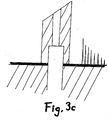
- an SOI wafer can be used, see Fig. 3b .
- the SiO 2 layer beneath the "device layer” will act as an etch stop, such that the height will be basically equal to the thickness of the device layer.
- Using an SOI wafer will also make possible the elimination of the residual sloping surface 30.
- the structure e.g. needle
- the structure can be given virtually any shape, such as round, elliptic, square, triangular, rectangular, polygonal etc., see Fig. 2b . If the mask defining the shape is rectangular or square, the end result will be a structure much resembling a knife-edge, and if the mask is round (the actual shape on the sloping surface would have to be elliptic of course), the end result will be a needle.
- the DRIE will remove material through said opening and will form a vertical channel in the structure.
- the shape of the channel i.e. its cross-section geometry can be varied at will, such as to render it circular, elliptic, square or rectangular, or polygonal by shaping the opening in the mask appropriately.
- the depth of the central channel through the structure will preferably be equal to the height of the structure, if the channel is made at the same time as the needle itself, which would be the normal way of doing it.
- the diameter of the central hole will then be of importance.
- a too narrow channel would restrict the rate of removal of material during the etch, and thus the etching rate might be slower than outside the needle, which of course would render the hole having a depth differing from the depth to which the surrounding etch reaches.
- this latter approach would be more time consuming, and would require alignment of patterns between steps, and most likely would not be an economically viable method, other than for very specific purposes.
- a channel extending all the way through the wafer is achieved by making a second hole from the back side, e.g. using DRIE.
- DRIE deep plasma etching
- a further advantage is that the hole from the backside can be made with a larger diameter, which means that the etching is faster (>2 times as fast), meaning higher through-put and thereby a cheaper process.
- the starting substrate for making protruding structures with obliquely cut tips comprises V-shaped recesses 40 or grooves in the wafer 12 instead of the protruding "ridges" discussed above, see Fig. 4 .
- Such recesses are made by masking a starting wafer so as to leave elongated slits mask material, i.e. a "negative" of the mask from the first embodiment. Subsequently this masked wafer is subjected to an anisotropic KOH-etch, which will act selectively on the exposed wafer material through said slit, thereby yielding a V-groove 40 wherein the sloping surfaces correspond to the ⁇ 111 > planes of the crystalline wafer.
- the wafer now comprising a plurality of V-grooves, is appropriately masked, suitably using a resist that is sprayed on or spin deposited for achieving a uniform layer of resist, to define the geometry of the desired structure, analogously to the first embodiment.
- a resist that is sprayed on or spin deposited for achieving a uniform layer of resist
- FIG. 5 the cured mask portions 50 defining the desired needle are shown.
- a DRIE etch follows whereby wafer material are etched away to form vertically protruding structures, e.g. needles 60.
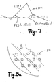
- the starting substrate has a crystal orientation different from standard. Normally the wafer surface would correspond to the ⁇ 100 plane. However, if the wafer is cut from the single crystal "ingot" at an angle deviating from the ⁇ 100> surface, which is referred to as an "off-cut" angle, the crystal planes determining the inclined surfaces during the isotropic etch, will be exposed at an angle the will differ from the 54,7° ( ⁇ 111> plane) by said "off-cut”-value. This is illustrated in Fig. 7a . The "off-cut" angle is normally 5-15°. Note however that it will still be the ⁇ 111 > plane that forms the inclined surface.
- the methods according to the above described embodiments will generate needles the inclined tip surfaces of which will have an angle differing from the ⁇ 111 > angle (i.e. 54,7°) by the "off-cut" value, as shown in Fig. 7b .
- needles can be made from substrates having no inclined starting surfaces, i.e. a conventional flat wafer is used as starting substrate.
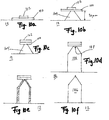
- the mask pattern can consist of square patches of e.g. SiO 2 Si x N y 80, as schematically shown in Fig. 8a .
- Applying a wet anisotropic etch e.g. KOH
- KOH wet anisotropic etch
- the sloping walls correspond to e.g. ⁇ 111 > planes of the wafer crystal.
- the mask will have to be very accurately orientated with respect to the orientation of crystal planes in the wafer. If the orientation is incorrect, the KOH etch will expose other crystal planes than the ⁇ 111> planes, namely planes like ⁇ 411> and ⁇ 311>. In such a case, the intersections between ⁇ 111 > planes will be "rounded off" and the end result will resemble the shape shown in Fig. 8d , i.e. a polygonal pyramid. In particular this latter case will give rise to round tips, as opposed to the square tips resulting in Fig. 8c .
- the degree of "rounding off” strongly depends on the etch that is used. For KOH there is a large degree of freedom on rounding due to the etching speed ratio ⁇ 411>/ ⁇ 100>. The speed strongly depends on concentration of the etching media.
- a dry anisotropic etch i.e. independent of crystal plane
- etch the base i.e. the vertical pillars are made, and the result will be the structure shown in fig. 8g .
- the tip of the needle When the mask 80, i.e. the pattern defining the needles, has been removed etching, the tip of the needle will not be pointed, but instead it will exhibit a top surface which is square, see Fig. 8c .
- an oxidation can be performed before removing the mask, by heating in an oxygen atmosphere, thereby oxide 82 will grow inwards under the mask 80, and when the oxide from different directions meet under the mask the intersection 84 between the oxide layers will cause the tip to become pointed.
- This method enables the manufacture of solid needles having a square base using a single mask.
- a rotationally symmetrical pyramid needle can be obtained by KOH etch without corner compensation.
- An example is shown in Fig. 8e .
- a mask is positioned on a wafer, the mask being similar to that used for making the needles of figs. 8c-d . However, in this case the mask is rotated 45° towards the wafer flat (i.e. the alignment feature provided on the wafer showing crystal orientation) on a (100) silicon wafer.
- a first mask 90 having a shape generally resembling an "X" is provided on a planar wafer, Fig. 9a , and a KOH etch is applied.
- the legs 92 of the "X" form corner compensation structures, and will have the effect of protecting the wafer material during the etch such that the unwanted crystal planes (e.g. ⁇ 311> and ⁇ 411> etc.) will not be exposed, thereby avoiding the problem of "rounded off” corners. This will result in a near perfect pyramid shown in Fig. 9b .
- lithography e.g. photoresist
- resist 94 is applied to the wafer comprising protruding pyramids, the desired geometry is exposed onto the resistand developed.
- Figs. 9c 1 and 9d 1 show an example wherein the entire pyramid iscovered with a "square shaped" resist layer
- Figs. 9c 2 and 9d 2 show the case where the resist is given a circular shape.
- two masks are provided on a flat substrate.
- a first "X"-shaped mask 100 (like the mask 90 in fig.9a ) is applied (see Fig 10a ), suitably by the deposition of SiN, or by providing a thin SiO 2 layer.
- a second mask 102 defining the base geometry (square or circular etc.) is applied, suitably an oxide is used (e.g SiO 2 that is thermally oxidized), but SiN can also be used.
- a KOH etch is applied to make a pyramid structure 104, suitably the pyramid will be approx. 30 ⁇ m high, as shown in Fig. 10b .
- the wafer is subjected to a "blank etch" which removes the first mask (SiN) but leaves the second mask very nearly unaffected.
- the result is the structure shown in Fig. 10c .
- corner compensation structures i.e. the "legs” of the "X” shaped structure
- a DRIE etch would result in "wings" extending out from the central body portion of the needle, a feature which could be beneficial for enhancing penetration performance.
- a DRIE etch is performed on the structure obtained and shown in fig. 10c , which will remove material in the vertical direction independent on crystal plane orientation, as shown in Fig. 10d . This will result in a vertically protruding needle 106 having a base geometry corresponding to the second mask shape.
- the tip at this stage in the process is covered by a mask 100, 102 which will cause the tip to have a flat top surface 108, i.e. it is not as sharp as desired.
- a local thermal oxidation is performed, see Figs 8e-f and Fig. 10e , and finally the oxide is stripped off, to leave a pointed needle 106, Fig. 10f .
- a "blank etch" of the oxide removes all oxide present on the wafer.
- SOI wafers Silicon On Insulator wafers
- the height can be controlled to a very high degree of accuracy, in particular the needles can be made to have a very uniform height, since the thickness of the device layer which extends down to the insulator 112 (SiO 2 ) is known to high accuracy.
- the insulator layer of the SOI wafer will function as an etch stop layer.
- the bottom layer is referred to as a handle layer 114.
- the buried oxide layer in the SOI wafer allows "over-etch” using DRIE for e.g. removing "grass” (see discussion in connection with Fig. 3c ).
- FIG. 11b-c This is illustrated in Fig. 11b-c , wherein an SOI wafer, after having been processed (patterning and isotropic KOH etch) to exhibit ridges wherein e.g. ⁇ 111 > planes are exposed, is patterned with masks 116 at different levels on at least one of the inclined surfaces 118 ( Fig. 11b ). Applying a DRIE etch will remove material in the vertical direction down to the etch stop (insulator) layer, to result in two needles 119a, 119b of different height, and both having obliquely cut tips, Fig. 11c .
- the structure/ configuration according to Fig. 11c can be used for the penetration of the skin, whereby the longer needle can be used to stimulate nerves, whereas the shorter needle will not reach down to the nerves and can be used for other purposes.
- both needles of Fig. 11c could be made to be hollow, by employing any of the methods previously described herein, in which case e.g. the longer needle could be used for the purpose of analyzing blood or glucose in blood vessels, at the same time the shorter needle could be used for injecting e.g. insulin or other medicaments in the skin.
- a particular application of the use of the methods according to the present invention, specifically employing the SOI wafer approach as discussed above, is to make electrically isolated groups of needle arrays. Such groups of arrays are suitable for e.g. making impedance measurement chips.
- This application is the subject matter of a copending Swedish patent application No. 05XXXXX-X (Title: “Needle arrays for impedance measurements") filed on the same day as the priority application to the present application, in the name of SciBase AB.
- a problem that exists in prior art methods employing DRIE machines is that an etch sequence of isotropic-anisotropic-isotropic etch (see Boisen et al and Stemme et al, supra ) is difficult to control from a process point of view. Namely, the first isotropic etch will vary across the wafer, i.e. different results will be obtained at the edges and at the centre, respectively. Near the edges of the wafer the etch rate in the vertical direction will be higher than at the centre, see Fig. 12a . The result will be longer and more pointed needles (left) at the edges.
- the first isotropic etch will also vary in dependence of how the pattern is designed or configured. Namely, masks defining e.g. individual needles that are closely spaced will have a higher etch rate in the vertical direction than in a case with masks that are not so closely spaced, see Fig. 12b . The result is that "dense" patterns will yield higher needles than less "dense”.
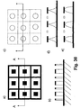
- Fig. 36 shows a top view of a part of a wafer where blocks of silicon has been provided surrounded by thin walls by an anisotropic DRIE etch.
- Fig. 36b is a cross-section at A-A in fig. 36a .
- Fig. 36c illustrates in a top view of the result after isotropic etch, e.g. a wet HNA or a dry DRIE etch.
- Fig. 36d is a cross-section through Fig. 36c after one type of HNA etch yielding very pointed tips, and Fig. 36d is the result of another HNA etch yielding more blunt ended needles.
- the present invention therefore relates to a novel process sequence for eliminating this "location effect", i.e. the invention provides a method that will generate uniformly high needles, and needles that are uniformly pointed, regardless of where on the wafer needles are located, or how close the individual masks are laid out on the wafer.
- the novel method comprises only two etching steps, as opposed to the above mentioned iso-aniso-iso DRIE sequence, namely a first dry anisotropic etch followed by a wet isotropic etch (HNA etch; Hydrochloric acid:Nitric acid:Acetic acid).
- a dry anisotropic etch to a suitably patterned substrate (e.g. a pattern defining circular needles) will result in the structure shown in Fig. 13a , since the etch rate for the dry anisotropic etch is essentially the same in the vertical direction independent on pattern configuration or the location on the wafer of the individual pattern elements.
- the wet isotropic etch is applied to the structure obtained in Fig. 13a .
- the invention makes use of the fact that the wet isotropic is not 100 % isotropic, but will actually etch slightly faster at the top of the "pillar" than at the bottom, resulting in the structure shown in Fig. 13b .
- the tip can then be sharpened in the same way as described in connection with Fig.10e .
- a method for making uniformly high and preferably uniformly pointed needles comprising only two etching steps, namely a first dry anisotropic etch applied to a patterned substrate (e.g. a pattern defining circular needles), followed by a wet isotropic etch (e.g. HNA etch; Hydrochloric acid:Nitric acid:Acetic acid), which etches slightly faster at the top of the "pillar" than at the bottom.
- a patterned substrate e.g. a pattern defining circular needles
- a wet isotropic etch e.g. HNA etch; Hydrochloric acid:Nitric acid:Acetic acid
- the tip is subsequently sharpened.
- a still further aspect of the invention relates to the problem of achieving electrical connections between areas of a chip/wafer with various structures provided on the surface of said chip/wafer.
- the structures can be needles, or arrays of needles, made by any of the methods described above, or by any of the prior art methods. It is desirable to provide areas having suitable properties for packaging, soldering, "flip-chip” mounting, wire bonding etc.
- a metallization layer/ metal layer 140a, 140b is provided on the top and bottom surfaces, respectively, of a chip/wafer 12. Suitable methods are evaporation techniques, sputtering, plating, CVD and other methods available. In this case electrical connection is through the chip/wafer bulk, see Fig. 14a .
- Such a metal layer can comprise (AlSiCu) + Ni + Au, a metal combination which is well suited for soldering or "flip-chip” mounting.
- Ag and AgCl are suitable for applications wherein the needles are to be used as electrodes (EEG, ECG etc.). Ag and AgCl are suitable. AgCl is particularly useful and preferred due to its good biopotential signal pick-up capability, and is also compatible with current medical requirements.
- Ti or TiW combined with Au or Al(AlSiCu) are suitable metals.
- Fig. 14b which could be usable when the wafer material does not exhibit electrical conductivity, similar or the same metallizations as in the first embodiment can be used in combination with one or more through holes 142, the inner surfaces 140c of which also are metallized. Thereby connection between the top and bottom surfaces will occur through said holes.
- the holes can be made by a number of different methods, e.g. wet etching, dry etching, drilling, laser, EDM etc.
- a variation of the second embodiment is to apply metallization layers to the edges 140d of the chip/wafer, such that connection is via the edges between top and bottom surfaces, see Fig. 14c .
- This in particular applicable whe SOI wafers have been used since there must be provided a "by-pass" connection to bridge the insulating material.
- a method invented by the applicants and disclosed in pending international patent application WO 04/084300 can be used.
- This method involves the provision of trenches 150 (i.e. deep recesses) extending all the way through the chip/wafer 12 from top to bottom surface, and filling said trenches with an insulating material 152, as illustrated in Fig. 15a .
- the trenches can be left as is, i.e. without filling in which case the air will function as the insulator.
- the disclosures of said application and patent are hereby included in their entirety by reference.
- a wafer having been provided with trenches as mentioned above is used as the starting substrate for making the desired structured wafer.
- the chip/wafer is conductive, i.e. electrical connection is achieved through the bulk material.
- the electrical through connections would be made by the method(s) described in connection with Fig. 14a-c .
- the insulating material 152 in the trenches 150 protrudes slightly above the base surface 154 from which the needles 156 protrude. This is because a pure silicon wafer has been used initially, and the trenches must than be etched to a desired depth with a small margin, such that it is ascertained that the discrete portions of the wafer carrying the needle structures actually will be isolated from each other.
- FIG. 15b illustrates another variant wherein an SOI wafer 14, comprising a buried insulating SiO 2 layer 158 is used initially for processing.
- the methods according to the above mentioned patent can be used to provide "vias" 155, i.e. electrical through-connections from the back-side, through the bottom silicon layer and through the insulator 158 into the front side material.
- vias made in any other way are usable for this embodiment, as long as they meet the requirements of the embodiment.
- other methods can be used, such as the method disclosed in Swedish patent application SE-0600214-1 "Molten metal via” (Silex Microsystems).
- the vias are filled with a conductive material (i.e. metal, doped semiconductor etc.).
- the "vias” should only just about extend through the insulator material, suitably not more than a few ⁇ m, suitably 1-5 ⁇ m.
- the "vias” are made by pre-processing of the wafer, i.e. a wafer already having been provided with vias is used as a starting wafer.
- electrically isolated discrete portions of the wafer caryring array groups are made by providing recesses 157 in the front side base material that extend down to and/or through the insulator layer 158 in the SOI wafer.
- These recesses can be made by sawing, in which case the depth of the recesses should be sufficiently large to extend through the insulator. This is because the sawing process generates particulate material that could cause short-circuits between the array groups. Thus, a margin of about 25 ⁇ m down below the insulator layer 158 is required.
- such insulating recesses can be made by etching, laser cutting or any other method that is capable of providing recesses of desired depths and widths.
- the insulator layer could act as an etch stop in which case the recesses will only extend down to said layer.
- the recesses can be filled with insulating material, such as an oxide.
- the back side of the finished wafer should be provided with a conductive layer 159, e.g. a metallization, such as the ones described above, i.e. a metal layer comprising (AlSiCu) + Ni + Au for soldering or "flip-chip” mounting (currently it is common to use lead solder, but there is a strive to go away from lead. Instead AuSn or AgSn are possible materials), or for wire bonding Ti or TiW combined with Au, or Al(AlSiCu).
- a conductive layer 159 e.g. a metallization, such as the ones described above, i.e. a metal layer comprising (AlSiCu) + Ni + Au for soldering or "flip-chip" mounting (currently it is common to use lead solder, but there is a strive to go away from lead. Instead AuSn or AgSn are possible materials), or for wire bonding Ti or TiW combined with Au, or Al(AlSiCu).
- sawing, etch or laser cutting can be used also for making the bottom-side recesses 153, care being taken to ascertain that the recess 153 extend at least up to the insulator layer 158 in the SOI wafer. If sawing is used to provide the recess, it should preferably be made so as to extend slightly into the silicon on the top side, as can be seen in Fig. 15b .
- trenches for providing vias and/or insulating separation members are advantageous in that it will become possible distribute groups or arrays of needles in an arbitrary manner.
- trenches according to the above described methods see the cited patent
- the geometry will only be restricted by the limitations inherent in the patterning/etching processes that are available. For example it will become possible to manufacture round/circular chips. Round chips are particularly advantageous for applications with emitting tips. In the case where sawing is used to separate such groups, only rectangular shapes are possible.
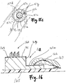
- Fig. 15c illustrates an exemplary embodiment wherein a round chip having micro-needles is made.
- the chips can be provided with metal on the back-side, for the purpose of enabling soldering, and if solder bumps are provided, the circular chips are ideal for flip-chip mounting.
- a needle array chip In a case where a needle array chip is to be attached to a circuit-board, it may not be suitable to have contact pads for connection to other parts of the circuit-board on the bottom-side of the chip. Also, it is important that the needles actually constitutes a protruding portion, located at a higher level than any surrounding structure. If not, the needles could simply not be used as intended, e.g. for penetration of the skin.
- the needle array 160 is made by any of the processes described herein previously. Then, instead of attaching connections at the bottom-side, the chip is provided with a stepped-down portion 162, as shown in Fig. 16 , i.e. with a surface 162a located adjacent the area carrying the needle array 160 but at a lower level than the base surface 161 of the needle array 160.
- a step portion can easily be made by suitable processing, e.g. a lithographic patterning/etching process, or by sawing. This will not be described in detail, since the skilled man would immediately realize how to obtain it.
- the entire upper surface of the chip including the vertical wall 163 extending between the upper base surface 161 and the horizontal surface 162a of the stepped-down portion is metallized 164, such there will be electrical connection between the array of micro-needles 160 and the surface 162a of the stepped-down portion.
- Metallization is required for wire bonding, but it is possible to make electrical contact directly onto silicon by using conductive glue.
- the chip can be attached to a circuit-board 165, e.g. by gluing.
- Wires 166 can be attached to the chip at the stepped-down portion, and the wires are protected 167by so called globbing, by providing "glob tops" (glob encapsulation).
- the chip can be placed with the needles pointing upwards during attachment of wires, which is advantageous in that there will be lees risk for damaging the needles during the mounting procedure in a manufacturing facility.
- Figs. 17a-b see also Fig. 2c
- the wafer is attached to a glass substrate/wafer, 171 suitably by anodic bonding.
- the glass wafer will provide an electrical insulator that separates the arrays electrically (see further below). It also functions as a carrier that exhibits the required strength.
- a stepped-down portion 172 is provided by sawing or by etching, as described in detail above.
- the "shelf" 173 thus made will form the base for the provision of wire bonding at a later stage in the processing.
- the entire wafer is metallized and preferably care is taken to ascertain that also the vertical walls 174 of the stepped-down portion is metallized to provide good electrical connection between the needle base (upper surface) and the stepped-down portion forming the bonding area. This is however not strictly necessary if the silicon wafer itself is sufficiently conductive such that electrical connection between needles can be achieved through the wafer bulk material. However, if an SOI wafer is used a "by-pass" connection must be provided (see below, Fig. 19 )
- the groups of needle arrays on one individual chip are separated electrically from each other by sawing or laser cutting recesses 175 down through the silicon bulk material and slightly down into the glass bottom substrate. Thereby electrically insulated groups of needle arrays 170 are provided, see Fig. 17b .
- an SOI wafer can be used as a starting substrate, in which case there will be no need for bonding the silicon wafer to a glass wafer. Instead, the buried oxide layer 180 in the SOI wafer will provide the required electrical insulation between array groups 182, see Fig. 18 .
- the SOI wafer should in this embodiment have a device layer that is 150 - 200 ⁇ m thick, in order to enable the manufacture of needles of appropriate size, and a handle layer that is approximately 1000 ⁇ m thick, in order to provide the necessary mechanical strength.
- a stepped-down portion 184 is provided by sawing or etching, and the entire wafer is metallized.
- the vertical wall 186 of the stepped-down portion 184 is appropriately coated with metal, since the electrical current will flow only through the metal coating.
- the exposed part of the insulator layer 180 on the vertical wall 186 between device layer and handle layer is covered with metal, since otherwise there would be no electrical connection between the needles and the horizontal surface 188 of the stepped-down portion where wires are to be bonded.
- the array groups 182 are separated from each other by sawing or etching a recess 189, like in the previous embodiment. In this case it is only necessary that the recess be so deep as to have its lowest point below the metallization of the stepped-down horizontal surface 188.
- One advantage of using an SOI wafer, as described above, is that the needles can be made with highly accurate heights, since the oxide layer of the SOI wafer will act as an efficient etch stop.
- an SOI wafer having a thick device layer 190 and a thin handle layer 191 can be used, see Fig. 19 .
- the insulator layer 192 can be of the same thickness as for the previous embodiment. Thereby, essentially the same process steps as in the embodiment according to Fig. 18 will be carried out. However, in this case it will not be equally important to metallize the entire wafer. This is because when the separating recess 193 is made, the buried insulator layer 192 of the SOI wafer will provide the necessary insulation between the array groups 195, and the electrical current can be drawn through the bulk silicon material. Thus, there is no need for vertical wall metallization at the stepped-down portion.
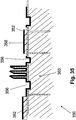
- Fig. 25 and Fig. 26 illustrates two embodiments of the grouping of needles 252 on an impedance chip 250.
- the needles are provided on surface areas circular cylindrically enclosed by insulating oxide (so called vias 254), and in Fig. 26 the provision of insulating oxide structures 264 extending vertically through the wafer 260 and across the entire width so as to provide discrete blocks on which the needles 262 are provided.
- Fig. 27 shows a cross-section along A-A in Figs. 25 and 26 .
- the insulation between needle groups is also required in order to prevent the skin, in contact with which the entire chip 270 is brought, from short-circuiting the needles. This is illustrated in Fig. 28 , where it is clearly seen that if the surface between the arrays of needles 272 were electrically conducting, a short-circuit would inevitably occur (in the figure there is an oxide layer 274 present).
- Fig. 30 is a cross-section through a chip clearly showing grooves 300 extending down through the oxide 302 and into the wafer bulk silicon 304.
- a shadow mask 312 is provided over the chip 310, effectively exposing only the needles 314 and preferably only a part of the groove 316, and effectively shading those parts of the chip that still must be insulating 318.
- this mask is a separate object placed over the structure to be processed. It is well known to the skilled man how to align the shadow mask pattern relative to the needle on the wafer by using e.g. wafer bond aligners. Alignment tolerances in the range of a few microns to a few tens of microns are easily achievable. I.e. it is not deposited as is the case with masks based on e.g.
- Metal 319 is now deposited through the shadow mask, e.g. by sputtering or evaporation or any other suitable method. The metal will thereby cover the needles and the portion of the wafer that is exposed through the mask 312, forming a continuous layer over the exposed structures. The result will be an electrical connection between needles 314 and bulk wafer silicon 317, as shown schematically in Fig. 31 .
- the sawing method is only applicable to the embodiment according to Fig. 26 wherein the delimiting, vertical oxide walls inside the chip are straight, essentially "planar" structures.
- Fig. 25 With circular vias the sawing is if not impossible, at least extremely difficult to envisage, however blasting, laser cutting or drilling could be used. Thus, for this case a lithographic/etching procedure is preferable, illustrated in fig. 32 .
- a resist 322 is applied to the wafer, taking great care to protect the needle tips with resist, and a suitable pattern is provided on the resist to open up holes or grooves in the resist through which an etchant can act through the mask and provide a slight over-etch down into the silicon. After removing the remaining resist, the result will resemble the structure shown in Fig. 30 , however the groove can be made slightly shallower than the groove obtained by sawing or other non-photo-lithographic techniques.
- An alternative to using the shadow mask is a procedure based on lithography and etching.
- a resist is applied to the wafer over its entire surface.
- the resist is applied by spraying, spinning, dip coating, laminating or roller coating, or electro-depositing. In this process it is very important that the tips of the needles be adequately protected by the resist.
- the resist is then patterned to provide the tracks for etching the grooves. An etch is applied through the resist pattern to remove the oxide and to provide an overetch down into the silicon.
- the patterning can be made to fit essentially any geometry of the needles and vias, e.g the configuration shown in Fig. 26 .
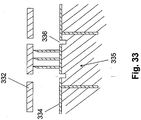
- a further alternative embodiment for providing the necessary grooves is to provide a shadow mask as shown in Fig. 33 , and to apply a suitable etch (e.g. dry reactive ion siliconoxide etch using high biasing) through the mask.
- a suitable etch e.g. dry reactive ion siliconoxide etch using high biasing
- the etch will remove oxide to expose the silicon and preferably slightly over-etch down into the silicon.
- the starting point for the procedure is a structure as shown in Fig. 30 or Fig. 32 , i.e. a wafer where grooves have been made by sawing or etching.
- a layer of metal is deposited by suitable methods (e.g. sputtering, evaporation or similar methods).
- a shadow mask is positioned above the wafer so as to expose the areas between needle arrays where it is desirable to provide the insulator.
- Insulator e.g. different silicon oxide, silicon nitride and similar compounds
- sputtering, evaporation PECVD through the mask.
- a sawing operation is performed at the locations indicated by dotted lines in Fig. 34 .
- the groove obtained must extend through the oxide layer and into the silicon, whereby the electrical connection in the metal layer is disrupted.
- a lift-off procedure is performed as follows.
- a resist is applied to the wafer, e.g. by spinning.
- a standard lithographic procedure is performed to pattern the resist for defining the insulating areas between the needle arrays, i.e. the resist is removed on the areas where the needles are located.
- a metal layer is deposited over the entire wafer. It should be noted that the resist, having a finite thickness, will exhibit vertical walls at the edges of the resist layers. During the metal deposition no metal will be deposited on these vertical walls.
- a lift-off is performed, i.e. the wafer is exposed to a suitable solvent. To dissolve the resist, whereby the metal deposited on top of the resist will also be removed, whereas the metal deposited on the needles and adjacent portions of the wafer will be left. Thus, electrical connection between the needles and the silicon in the grooves.
- hollow needles made according to the present invention are very well suited for the delivery of fluids, such as drugs, to patients through the skin.
- fluids such as drugs
- the fluid has to be transported from some reservoir, external to the micro needle device, and fed into the chip for subsequent delivery through the plurality of needles of an array.
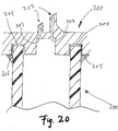
- Fig. 20 there is shown an example of how such a connection can be designed in accordance with a further aspect of the invention.
- fluids are normally delivered through flexible tubing 200 having diameters in the mm scale, and thus have to be connected to a chip 201 with connectors of the same dimensions.
- a solution to this is to provide a chip having a plurality of hollow needles 202, wherein the inlets 203 to each needle 202 on the back side of the chip 201, are enclosed by a circular recess 204 having a width corresponding to the thickness of the tubing 200 material, thus having an inner and outer diameter corresponding to the inner and outer diameter, respectively of the tubing 200.
- the tubing is inserted into said recess 204, preferably in a relatively tight fit, but secured in place suitably by gluing 205.
- the invention relates to a method of making protruding members, e.g. needles, having side openings, and closed tips.
- protruding members e.g. needles
- Such needles and manufacturing thereof are disclosed in WO 2003/015860 (Stemme et al ).
- the present process comprises as an initial step the provision of an inclined surface, using any of the methods described previously herein.
- a pyramid-like structure 210 having surfaces exposing the ⁇ 111> planes is made by KOH etching after appropriate masking.
- the structure can be other than pyramidal; e.g. if an elongated structure is made it will resemble a ridge rather than a pyramid.
- a hole 212 is made from the backside, matched to the pyramid/ridge such that the hole is located essentially centred below the apex of the ridge. This approach will give a structure having side openings in all four directions, see Fig 24a .
- a double lithography ( Figs. 22-23 ) is performed to make two masks, one on top of the other.
- a first mask is made by oxidation to provide an oxide layer that subsequently is appropriately patterned, to provide a pattern of first masks, and then a second mask can be made by depositing a second oxide on top of the first, or by depositing resist on top of the first oxide layer, in a suitable pattern.
- the cross-section through the mask structure will be as shown in Fig. 22a , i.e. the first mask (oxide) 220 is larger than the second mask (oxide) 222, and thus the first mask will define the base geometry of the protrusion (needle), whereas the second mask will define the final geometry of the side-opened needles.
- the cross-section through the wafer and mask structure will be as shown in Fig. 23a , i.e. the second mask 230 (resist) is larger than the first mask (oxide) 232 and covers it, i.e. the second mask will define the base geometry of the protrusion (needle), and the first mask will define the final geometry of the side-opened needles.
- the smaller masks will cover an area in the horizontal plane that is slightly smaller than the area of the circular hole made from the bottom of the substrate, i.e. at least one segment of the circumference of the hole will not be covered by the mask. If several side openings are desirable, the mask must leave a plurality of segments uncovered by the mask, see Fig. 24c .
- the hole from the back side will be given a shape in cross-section that is not circular (see Fig. 24d ).
- a cross-shaped section will enable stronger structures between the openings and connecting the base and the top of each needle.
- any other geometry can be used as long as the desired openings are created in the final structure.
- a DRIE etch is applied to the double patterned substrate, which will remove material selectively in the vertical direction, and independently of crystal plane orientation, for making the "pillars" of the needles, resulting in the structures shown in Figs. 22b and 23b .
- a "blank etch” is performed, i.e. oxide is removed down to the substrate. Since the second mask is on top of the first mask, thereby increasing the oxide layer to the double thickness, a portion of the first mask located under the second mask will remain, thereby defining a small mask.
- the resist is simply dissolved away using an appropriate solvent, thereby exposing the first mask defining a mask with the same geometry as the mask in the first alternative.
- a DRIE is applied which will remove material in the vertical direction down to a selected distance, as shown in Fig. 24b , where about half of the pillar height is removed in this step. This will open up side openings, by virtue of the fact that the circumference of the circular hole will extend beyond the limits of the area defined by the small mask.
- Figs 24c and 24d this relationship is schematically illustrated in a top view where the circular hole is indicated with broken lines and the small mask is shown to cover a portion of the pyramid only.
- Fig. 24a shows a final structure in perspective.
Landscapes
- Health & Medical Sciences (AREA)
- Life Sciences & Earth Sciences (AREA)
- Engineering & Computer Science (AREA)
- Public Health (AREA)
- Veterinary Medicine (AREA)
- Biomedical Technology (AREA)
- Heart & Thoracic Surgery (AREA)
- Animal Behavior & Ethology (AREA)
- General Health & Medical Sciences (AREA)
- Medical Informatics (AREA)
- Hematology (AREA)
- Biophysics (AREA)
- Molecular Biology (AREA)
- Physics & Mathematics (AREA)
- Surgery (AREA)
- Pathology (AREA)
- Manufacturing & Machinery (AREA)
- Cardiology (AREA)
- Nuclear Medicine, Radiotherapy & Molecular Imaging (AREA)
- Radiology & Medical Imaging (AREA)
- Dermatology (AREA)
- Neurology (AREA)
- Neurosurgery (AREA)
- Orthopedic Medicine & Surgery (AREA)
- Anesthesiology (AREA)
- Micromachines (AREA)
- Cold Cathode And The Manufacture (AREA)
- Drying Of Semiconductors (AREA)
Abstract
Claims (16)
- Procédé de fabrication d'éléments verticalement saillants sur un substrat, lesdits éléments présentant une pointe comprenant au moins une surface inclinée et une partie de corps allongée s'étendant entre ledit substrat et ladite pointe, le procédé comprenant :un premier processus de gravure anisotrope dépendant du plan cristallin, formant ladite/lesdites surface(s) inclinée (s) ; etun deuxième processus de gravure anisotrope ne dépendant pas du plan cristallin, formant ladite partie de corps allongée ; etle fait de mettre sélectivement en forme ladite/lesdites surface(s) inclinée(s) afin d'aboutir à la réalisation d'un motif définissant une géométrie de base pour l'élément saillant.
- Procédé de fabrication d'éléments verticalement saillants sur un substrat tel que revendiqué dans la revendication 1, le procédé comprenant les étapes suivantes qui consistent :à fournir un substrat pouvant être gravé ayant une première face et une deuxième face dont au moins une face est monocristalline ;à mettre en forme ledit substrat sur ladite face monocristalline pour former un masque de gravure afin d'exposer ses zones sélectionnées ;à mettre en oeuvre le premier processus de gravure anisotrope à travers ledit masque pour exposer un plan cristallin sélectionné dudit substrat monocristallin afin de fournir au moins une surface inclinée, la première gravure anisotrope dépendant du plan cristallin ;à mettre en oeuvre le deuxième processus de gravure anisotrope pour enlever de la matière essentiellement dans la direction verticale seulement de manière à laisser des éléments verticalement saillants selon ledit motif.
- Procédé tel que revendiqué dans la revendication 2, dans lequel l'étape de mise en forme du substrat comprend en outre l'alignement du motif avec des orientations cristallines sélectionnées dudit substrat.
- Procédé tel que revendiqué dans la revendication 2 ou 3, dans lequel l'étape de mise en forme comprend en outre l'utilisation, pour le masque, d'un matériau qui résiste à la gravure qui fournit la surface inclinée.
- Procédé tel que revendiqué dans la revendication 4, dans lequel le masque comprend des zones ayant au moins un bord aligné avec l'orientation cristalline de la plaquette.
- Procédé tel que revendiqué dans la revendication 5, dans lequel le masque comprend des zones discrètes de matériau de masque pour définir un élément saillant ayant des surfaces inclinées.
- Procédé tel que revendiqué dans la revendication 2, dans lequel ledit masque comprend des zones ouvertes exposant la plaquette pour définir des creux ayant des surfaces inclinées.
- Procédé tel que revendiqué dans la revendication 1, dans lequel l'étape de mise en forme de la/des surface(s) inclinée(s) comprend le fait de fournir une couche de masquage d'une épaisseur uniforme par pulvérisation ou rotation.
- Procédé tel que revendiqué dans la revendication 2, dans lequel le premier processus de gravure pour fournir la/les surface(s) inclinée(s) est mis en oeuvre en utilisant une gravure humide, de préférence sélectionnée parmi les techniques d'EDP, TMAH, NaOH, KOH acqueux, plus avantageusement la gravure est une gravure KOH.
- Procédé tel que revendiqué dans la revendication 2, dans lequel le deuxième processus de gravure pour fournir les éléments verticalement saillants est mis en oeuvre en utilisant une gravure DRI.
- Procédé tel que revendiqué dans la revendication 2, dans lequel le substrat est une plaquette SOI.
- Procédé tel que revendiqué dans la revendication 1, comprenant en outre les étapes qui consistent :à fournir un substrat pouvant être gravé présentant une première face et une deuxième face ;à mettre en forme le substrat sur la face monocristalline pour former un masque de gravure afin d'exposer des zones sélectionnées du substrat ;le premier processus de gravure anisotrope comprend l'application d'un processus DRIE à travers ledit masque ; età régler les paramètres de gravure de manière à provoquer un déplacement latéral incrémental des segments verticaux suivants générés à chaque incrément de gravure, de sorte à produire effectivement une surface en pente, la surface en pente étant "étagée" en une échelle microscopique, et ne suivant aucun plan cristallin.
- Procédé tel que revendiqué dans la revendication 1, dans lequel le motif définissant la géométrie de base pour la structure en saillie comprend une ouverture, moyennant quoi la deuxième gravure enlève de la matière à travers ladite ouverture pour former un canal vertical dans la structure.
- Procédé tel que revendiqué dans la revendication 1, dans lequel se trouve une étape supplémentaire de gravure après le masquage approprié du motif pour fournir une ouverture dans ledit motif, afin de créer un canal vertical.
- Procédé tel que revendiqué dans la revendication 13 ou 14, dans lequel un canal s'étendant tout le long de la plaquette est obtenu en réalisant un deuxième trou sur la face arrière, par exemple en utilisant le processus DRIE.
- Procédé tel que revendiqué dans la revendication 15, dans lequel le trou sur la face arrière est réalisé avec un plus grand diamètre, moyennant quoi la gravure est plus rapide.
Applications Claiming Priority (3)
| Application Number | Priority Date | Filing Date | Title |
|---|---|---|---|
| US75004705P | 2005-12-14 | 2005-12-14 | |
| SE0502760A SE531049C2 (sv) | 2005-12-14 | 2005-12-14 | Metoder för tillverkning av mikronålar |
| PCT/SE2006/050582 WO2007070004A2 (fr) | 2005-12-14 | 2006-12-14 | Procedes de fabrication de micro-aiguilles et applications de celles-ci |
Publications (3)
| Publication Number | Publication Date |
|---|---|
| EP1962679A2 EP1962679A2 (fr) | 2008-09-03 |
| EP1962679A4 EP1962679A4 (fr) | 2011-04-13 |
| EP1962679B1 true EP1962679B1 (fr) | 2012-04-11 |
Family
ID=38163360
Family Applications (1)
| Application Number | Title | Priority Date | Filing Date |
|---|---|---|---|
| EP06824640A Active EP1962679B1 (fr) | 2005-12-14 | 2006-12-14 | Procedes de fabrication de micro-aiguilles et applications de celles-ci |
Country Status (3)
| Country | Link |
|---|---|
| US (2) | US8308960B2 (fr) |
| EP (1) | EP1962679B1 (fr) |
| WO (1) | WO2007070004A2 (fr) |
Families Citing this family (68)
| Publication number | Priority date | Publication date | Assignee | Title |
|---|---|---|---|---|
| GB0402131D0 (en) | 2004-01-30 | 2004-03-03 | Isis Innovation | Delivery method |
| CA2587216C (fr) * | 2004-11-18 | 2014-11-18 | Nanopass Technologies Ltd. | Systeme et procede pour administrer un fluide a une barriere biologique souple |
| WO2009079712A1 (fr) | 2007-12-24 | 2009-07-02 | The University Of Queensland | Procédé d'application |
| WO2009097660A1 (fr) * | 2008-02-07 | 2009-08-13 | The University Of Queensland | Fabrication de timbre transdermique |
| CA2760680A1 (fr) | 2008-05-23 | 2009-11-26 | The University Of Queensland | Detection de substances a analyser par un timbre a micro-aiguilles avec des reactifs selectifs |
| US8860632B2 (en) * | 2008-09-08 | 2014-10-14 | Qualcomm Incorporated | Multi-panel device with configurable interface |
| CN102325563A (zh) | 2008-12-22 | 2012-01-18 | 昆士兰大学 | 贴剂制备 |
| FI20095433A0 (fi) | 2009-04-20 | 2009-04-20 | Valtion Teknillinen | Mikroneula |
| EP2275164A1 (fr) * | 2009-07-15 | 2011-01-19 | Debiotech S.A. | Micro-aiguilles à multicanaux |
| EP2462978A4 (fr) * | 2009-08-07 | 2013-01-02 | Medrx Co Ltd | Dispositif applicateur à microaiguilles de type à support d'aiguilles |
| WO2011135531A2 (fr) | 2010-04-28 | 2011-11-03 | Kimberly-Clark Worldwide, Inc. | DISPOSITIFS MÉDICAUX POUR L'ADMINISTRATION D'ARNsi |
| EP2563455A4 (fr) | 2010-04-28 | 2014-02-19 | Kimberly Clark Co | Procédé d'augmentation de la perméabilité d'une barrière épithéliale |
| MX345837B (es) * | 2010-04-28 | 2017-02-16 | Kimberly-Clark Worldwide Incorporated | Dispositivo para la entrega de un medicamento para la artritis reumatoide. |
| KR20130058012A (ko) * | 2010-04-28 | 2013-06-03 | 킴벌리-클라크 월드와이드, 인크. | 사출 성형된 마이크로니들 어레이 및 마이크로니들 어레이의 형성 방법 |
| WO2012006677A1 (fr) | 2010-07-14 | 2012-01-19 | The University Of Queensland | Appareil d'application de timbre transdermique |
| CN103458816B (zh) | 2011-03-29 | 2017-05-10 | 皇家飞利浦有限公司 | 基于功能成像的消融监测 |
| JP5995963B2 (ja) * | 2011-06-08 | 2016-09-21 | スリーエム イノベイティブ プロパティズ カンパニー | ポリマー連結ナノ粒子を含有するフォトレジスト |
| US11009788B2 (en) * | 2011-09-09 | 2021-05-18 | Centera Photonics Inc. | Method for manufacturing optical electrical module and substrate of an optical electrical module |
| EP2765927B1 (fr) | 2011-10-12 | 2021-02-24 | Vaxxas Pty Limited | Dispositif de distribution |
| US20170246439A9 (en) | 2011-10-27 | 2017-08-31 | Kimberly-Clark Worldwide, Inc. | Increased Bioavailability of Transdermally Delivered Agents |
| MX343262B (es) | 2011-10-27 | 2016-10-28 | Kimberly Clark Co | Administración transdérmica de agentes bioactivos de alta viscosidad. |
| ES2728143T3 (es) | 2011-11-11 | 2019-10-22 | Univ California | Estimulación transcutánea de la médula espinal: herramienta no invasiva para la activación del circuito locomotor |
| SE538018C2 (sv) | 2011-12-22 | 2016-02-09 | Silex Microsystems Ab | Isolering av mikrostrukturer |
| SE537869C2 (sv) | 2012-11-01 | 2015-11-03 | Silex Microsystems Ab | Substratgenomgående vior |
| WO2014105458A1 (fr) * | 2012-12-27 | 2014-07-03 | 3M Innovative Properties Company | Article avec micro-aiguilles creuses et procédé de fabrication |
| WO2014144785A1 (fr) | 2013-03-15 | 2014-09-18 | The Regents Of The University Of California | Stimulation électrique transcutanée multi-site de la moelle épinière pour faciliter le déplacement |
| US11185271B2 (en) | 2013-09-13 | 2021-11-30 | University Of Utah Research Foundation | Methods of making micro-molded electrodes and arrays |
| CA2925754C (fr) | 2013-09-27 | 2023-02-21 | The Regents Of The University Of California | Implication des circuits de la moelle epiniere cervicale pour recreer un controle volitif de la fonction manuelle chez des sujets tetraplegiques |
| US10751533B2 (en) | 2014-08-21 | 2020-08-25 | The Regents Of The University Of California | Regulation of autonomic control of bladder voiding after a complete spinal cord injury |
| EP3185946B1 (fr) | 2014-08-27 | 2019-10-09 | The Regents Of The University Of California | Réseau à multiples électrodes pour stimulation épidurale de moelle épinière |
| US11147954B2 (en) | 2015-02-02 | 2021-10-19 | Vaxxas Pty Limited | Microprojection array applicator and method |
| US20190022371A1 (en) * | 2015-08-06 | 2019-01-24 | The Regents Of The University Of California | Electrode array for transcutaneous electrical stimulation of the spinal cord and uses thereof |
| US11298533B2 (en) | 2015-08-26 | 2022-04-12 | The Regents Of The University Of California | Concerted use of noninvasive neuromodulation device with exoskeleton to enable voluntary movement and greater muscle activation when stepping in a chronically paralyzed subject |
| US10172558B2 (en) | 2015-09-10 | 2019-01-08 | University Of Utah Research Foundation | Structure and methodology for a shadow mask having hollow high aspect ratio projections |
| US11103259B2 (en) | 2015-09-18 | 2021-08-31 | Vaxxas Pty Limited | Microprojection arrays with microprojections having large surface area profiles |
| US20180264244A1 (en) | 2015-09-28 | 2018-09-20 | Vaxxas Pty Limited | Microprojection arrays with enhanced skin penetrating properties and methods thereof |
| US11097122B2 (en) | 2015-11-04 | 2021-08-24 | The Regents Of The University Of California | Magnetic stimulation of the spinal cord to restore control of bladder and/or bowel |
| KR101837680B1 (ko) | 2016-04-14 | 2018-04-19 | 정진수 | 중공형 마이크로 니들 제조 방법 및 그에 의해 제조된 중공형 마이크로 니들 |
| WO2018148844A1 (fr) | 2017-02-17 | 2018-08-23 | The University Of British Columbia | Appareil et procédés de maintien des fonctions physiologiques |
| US12109032B1 (en) | 2017-03-11 | 2024-10-08 | Biolinq Incorporated | Methods for achieving an isolated electrical interface between an anterior surface of a microneedle structure and a posterior surface of a support structure |
| AU2018241251B2 (en) | 2017-03-31 | 2024-06-27 | Vaxxas Pty Limited | Device and method for coating surfaces |
| US11045142B1 (en) | 2017-04-29 | 2021-06-29 | Biolinq, Inc. | Heterogeneous integration of silicon-fabricated solid microneedle sensors and CMOS circuitry |
| US12434068B2 (en) | 2017-05-23 | 2025-10-07 | The Regents Of The University Of California | Accessing spinal networks to address sexual dysfunction |
| EP3639010B1 (fr) | 2017-06-13 | 2025-08-06 | Vaxxas Pty Limited | Contrôle de la qualité de revêtements de substrats |
| GB201709668D0 (en) | 2017-06-16 | 2017-08-02 | Spts Technologies Ltd | Microneedles |
| DE20168827T1 (de) | 2017-06-30 | 2021-01-21 | Gtx Medical B.V. | System zur neuromodulierung |
| US10586751B2 (en) * | 2017-08-03 | 2020-03-10 | Advanced Semiconductor Engineering, Inc. | Semiconductor package device and method of manufacturing the same |
| EP4548954A3 (fr) | 2017-08-04 | 2025-07-30 | Vaxxas Pty Limited | Actionneur à stockage d'énergie mécanique élevé compact et à force de déclenchement faible pour l'administration de patchs à réseaux de microprojections (prm) |
| US12599337B1 (en) | 2017-08-08 | 2026-04-14 | Biolinq Incorporated | Method and system for confirmation of microneedle-based analyte-selective sensor insertion into viable tissue via electrical interrogation |
| US11992684B2 (en) | 2017-12-05 | 2024-05-28 | Ecole Polytechnique Federale De Lausanne (Epfl) | System for planning and/or providing neuromodulation |
| US12357828B2 (en) | 2017-12-05 | 2025-07-15 | Ecole Polytechnique Federale De Lausanne (Epfl) | System for planning and/or providing neuromodulation |
| US20190366068A1 (en) * | 2018-05-29 | 2019-12-05 | Zibo Tanwei Nanotechnology Co., Ltd. | Microneedle for biosensing and method of fabrication |
| US12478777B2 (en) | 2018-08-23 | 2025-11-25 | The Regents Of The University Of California | Non-invasive spinal cord stimulation for nerve root palsy, cauda equina syndrome, and restoration of upper extremity function |
| WO2020069564A1 (fr) * | 2018-10-02 | 2020-04-09 | WearOptimo Pty Ltd | Système pour déterminer un niveau de fluide dans un sujet biologique |
| EP3653256B1 (fr) | 2018-11-13 | 2022-03-30 | ONWARD Medical N.V. | Système de commande pour la reconstruction et/ou la restauration des mouvements d'un patient |
| CN109795978A (zh) * | 2018-12-26 | 2019-05-24 | 华中科技大学 | 一种微型空心硅针管阵列及其制作方法 |
| EP3695878B1 (fr) | 2019-02-12 | 2023-04-19 | ONWARD Medical N.V. | Système de neuromodulation |
| JP6850457B2 (ja) * | 2019-03-12 | 2021-03-31 | シンクランド株式会社 | 角質層採取方法 |
| EP3972683A4 (fr) | 2019-05-22 | 2023-11-08 | The Regents Of The University Of California | Neuromodulateur électrique transcutané de moelle épinière et ses utilisations |
| EP3824948A1 (fr) | 2019-11-19 | 2021-05-26 | ONWARD Medical B.V. | Système de planification et/ou de commande pour un système de neuromodulation |
| DE19211738T1 (de) | 2019-11-27 | 2021-09-09 | Onward Medical B.V. | Neuromodulationssystem |
| EP3827871A1 (fr) | 2019-11-27 | 2021-06-02 | ONWARD Medical B.V. | Système de neuromodulation |
| US20220031244A1 (en) | 2020-07-29 | 2022-02-03 | Biolinq Inc. | Continuous analyte monitoring system with microneedle array |
| EP4153276B1 (fr) | 2021-05-08 | 2025-12-10 | Biolinq Incorporated | Étection de défauts pour dispositif de surveillance continue d'analytes basé sur un réseau de micro-aiguilles |
| WO2023225540A2 (fr) * | 2022-05-18 | 2023-11-23 | Mekonos Inc. | Procédés de fabrication pour micro-aiguilles et outils à rapport d'aspect élevé |
| CN115285930B (zh) * | 2022-07-25 | 2024-07-23 | 武汉衷华脑机融合科技发展有限公司 | 一种微针与排线倒焊连接结构及其制备工艺 |
| EP4658168A2 (fr) | 2023-02-02 | 2025-12-10 | Biolinq, Inc. | Procédé pour une sensibilité de capteur améliorée d'un système de surveillance d'analyte continu à base de micro-aiguilles |
| US12623080B2 (en) | 2023-06-21 | 2026-05-12 | Onward Medical N.V. | Neuromodulation system |
Family Cites Families (13)
| Publication number | Priority date | Publication date | Assignee | Title |
|---|---|---|---|---|
| US4585991A (en) * | 1982-06-03 | 1986-04-29 | Texas Instruments Incorporated | Solid state multiprobe testing apparatus |
| DE4241045C1 (de) | 1992-12-05 | 1994-05-26 | Bosch Gmbh Robert | Verfahren zum anisotropen Ätzen von Silicium |
| DE69422234T2 (de) * | 1993-07-16 | 2000-06-15 | Matsushita Electric Industrial Co., Ltd. | Verfahren zur Herstellung einer Feldemissionsanordnung |
| US5591139A (en) | 1994-06-06 | 1997-01-07 | The Regents Of The University Of California | IC-processed microneedles |
| US5929521A (en) * | 1997-03-26 | 1999-07-27 | Micron Technology, Inc. | Projected contact structure for bumped semiconductor device and resulting articles and assemblies |
| US6503231B1 (en) | 1998-06-10 | 2003-01-07 | Georgia Tech Research Corporation | Microneedle device for transport of molecules across tissue |
| US6551849B1 (en) | 1999-11-02 | 2003-04-22 | Christopher J. Kenney | Method for fabricating arrays of micro-needles |
| WO2001052731A1 (fr) | 2000-01-21 | 2001-07-26 | Instrumentarium Corporation | Electrode medicale |
| US6533949B1 (en) | 2000-08-28 | 2003-03-18 | Nanopass Ltd. | Microneedle structure and production method therefor |
| SE0102736D0 (sv) * | 2001-08-14 | 2001-08-14 | Patrick Griss | Side opened out-of-plane microneedles for microfluidic transdermal interfacing and fabrication process of side opened out-of-plane microneedles |
| JP2003273155A (ja) * | 2002-03-18 | 2003-09-26 | Fujitsu Ltd | 半導体装置及びその製造方法 |
| SE526366C3 (sv) | 2003-03-21 | 2005-10-26 | Silex Microsystems Ab | Elektriska anslutningar i substrat |
| US7591806B2 (en) * | 2004-05-18 | 2009-09-22 | Bai Xu | High-aspect-ratio microdevices and methods for transdermal delivery and sampling of active substances |
-
2006
- 2006-12-14 EP EP06824640A patent/EP1962679B1/fr active Active
- 2006-12-14 US US12/097,448 patent/US8308960B2/en active Active
- 2006-12-14 WO PCT/SE2006/050582 patent/WO2007070004A2/fr not_active Ceased
-
2011
- 2011-10-21 US US13/278,890 patent/US8637351B2/en active Active
Also Published As
| Publication number | Publication date |
|---|---|
| EP1962679A2 (fr) | 2008-09-03 |
| EP1962679A4 (fr) | 2011-04-13 |
| US8308960B2 (en) | 2012-11-13 |
| US20120126392A1 (en) | 2012-05-24 |
| WO2007070004A3 (fr) | 2007-08-23 |
| WO2007070004A2 (fr) | 2007-06-21 |
| US20100006536A1 (en) | 2010-01-14 |
| US8637351B2 (en) | 2014-01-28 |
Similar Documents
| Publication | Publication Date | Title |
|---|---|---|
| US8308960B2 (en) | Methods for making micro needles and applications thereof | |
| US6511463B1 (en) | Methods of fabricating microneedle arrays using sacrificial molds | |
| EP1418977B1 (fr) | Microaiguilles pour administration de medicaments avec effraction minimale | |
| CN113855031B (zh) | 柔性微针电极及其制备方法 | |
| AU744470B2 (en) | Transdermal probe with an isotropically etched tip, and method of fabricating such a device | |
| CA2376285C (fr) | Dispositif a jeu de microaiguilles intradermiques | |
| US20040060902A1 (en) | Microprotrusion array and methods of making a microprotrusion | |
| EP1364396A2 (fr) | Reseau de microprotuberances et procedes de formation d'une microprotuberance | |
| US9919916B2 (en) | Manufacture of microneedles | |
| CN105217565B (zh) | 一种单晶硅空心微针结构的制作方法 | |
| JP2004524172A5 (fr) | ||
| JP2002079499A (ja) | 針形状物の作製方法および作製された針 | |
| CN112631425A (zh) | 一种微针阵列式脑机接口器件及其制备方法 | |
| WO2013095260A1 (fr) | Isolation de microstrustures | |
| CN110559553A (zh) | 一种可批量制造有孔无痛微针阵列芯片的制备方法 | |
| CN114795221B (zh) | 一种柔性微针电极及其制备方法 | |
| Shikida et al. | Fabrication of densely arrayed micro-needles with flow channels by mechanical dicing and anisotropic wet etching | |
| US20080230856A1 (en) | Intermediate probe structures for atomic force microscopy | |
| SE534509C2 (sv) | Metod för tillverkning av anordningar för elektriska mätningar | |
| CN113476735B (zh) | 一种空心微针阵列芯片及其制备方法 | |
| SE0950857A1 (sv) | Metod för tillverkning av anordningar för elektriska mätningar | |
| Xu et al. | Anodic-Bonding-Assisted Silicon Microelectrode Array For Neural Applications | |
| EP1544865B1 (fr) | Procédé de fabrication de sondes pour microscopie à force atomique | |
| CN113443603A (zh) | 一种超细空心微针芯片的制备方法 | |
| Pemba et al. | SU-8/silicon hybrid three dimensional intraneural electrode array |
Legal Events
| Date | Code | Title | Description |
|---|---|---|---|
| PUAI | Public reference made under article 153(3) epc to a published international application that has entered the european phase |
Free format text: ORIGINAL CODE: 0009012 |
|
| 17P | Request for examination filed |
Effective date: 20080703 |
|
| AK | Designated contracting states |
Kind code of ref document: A2 Designated state(s): AT BE BG CH CY CZ DE DK EE ES FI FR GB GR HU IE IS IT LI LT LU LV MC NL PL PT RO SE SI SK TR |
|
| A4 | Supplementary search report drawn up and despatched |
Effective date: 20110311 |
|
| GRAP | Despatch of communication of intention to grant a patent |
Free format text: ORIGINAL CODE: EPIDOSNIGR1 |
|
| DAX | Request for extension of the european patent (deleted) | ||
| GRAS | Grant fee paid |
Free format text: ORIGINAL CODE: EPIDOSNIGR3 |
|
| GRAA | (expected) grant |
Free format text: ORIGINAL CODE: 0009210 |
|
| AK | Designated contracting states |
Kind code of ref document: B1 Designated state(s): AT BE BG CH CY CZ DE DK EE ES FI FR GB GR HU IE IS IT LI LT LU LV MC NL PL PT RO SE SI SK TR |
|
| REG | Reference to a national code |
Ref country code: GB Ref legal event code: FG4D |
|
| REG | Reference to a national code |
Ref country code: CH Ref legal event code: EP |
|
| REG | Reference to a national code |
Ref country code: AT Ref legal event code: REF Ref document number: 552775 Country of ref document: AT Kind code of ref document: T Effective date: 20120415 |
|
| REG | Reference to a national code |
Ref country code: IE Ref legal event code: FG4D |
|
| REG | Reference to a national code |
Ref country code: DE Ref legal event code: R096 Ref document number: 602006028849 Country of ref document: DE Effective date: 20120606 |
|
| REG | Reference to a national code |
Ref country code: NL Ref legal event code: VDEP Effective date: 20120411 |
|
| REG | Reference to a national code |
Ref country code: AT Ref legal event code: MK05 Ref document number: 552775 Country of ref document: AT Kind code of ref document: T Effective date: 20120411 |
|
| LTIE | Lt: invalidation of european patent or patent extension |
Effective date: 20120411 |
|
| PG25 | Lapsed in a contracting state [announced via postgrant information from national office to epo] |
Ref country code: PL Free format text: LAPSE BECAUSE OF FAILURE TO SUBMIT A TRANSLATION OF THE DESCRIPTION OR TO PAY THE FEE WITHIN THE PRESCRIBED TIME-LIMIT Effective date: 20120411 Ref country code: FI Free format text: LAPSE BECAUSE OF FAILURE TO SUBMIT A TRANSLATION OF THE DESCRIPTION OR TO PAY THE FEE WITHIN THE PRESCRIBED TIME-LIMIT Effective date: 20120411 Ref country code: SE Free format text: LAPSE BECAUSE OF FAILURE TO SUBMIT A TRANSLATION OF THE DESCRIPTION OR TO PAY THE FEE WITHIN THE PRESCRIBED TIME-LIMIT Effective date: 20120411 Ref country code: IS Free format text: LAPSE BECAUSE OF FAILURE TO SUBMIT A TRANSLATION OF THE DESCRIPTION OR TO PAY THE FEE WITHIN THE PRESCRIBED TIME-LIMIT Effective date: 20120811 Ref country code: LT Free format text: LAPSE BECAUSE OF FAILURE TO SUBMIT A TRANSLATION OF THE DESCRIPTION OR TO PAY THE FEE WITHIN THE PRESCRIBED TIME-LIMIT Effective date: 20120411 Ref country code: CY Free format text: LAPSE BECAUSE OF FAILURE TO SUBMIT A TRANSLATION OF THE DESCRIPTION OR TO PAY THE FEE WITHIN THE PRESCRIBED TIME-LIMIT Effective date: 20120411 |
|
| PG25 | Lapsed in a contracting state [announced via postgrant information from national office to epo] |
Ref country code: PT Free format text: LAPSE BECAUSE OF FAILURE TO SUBMIT A TRANSLATION OF THE DESCRIPTION OR TO PAY THE FEE WITHIN THE PRESCRIBED TIME-LIMIT Effective date: 20120813 Ref country code: GR Free format text: LAPSE BECAUSE OF FAILURE TO SUBMIT A TRANSLATION OF THE DESCRIPTION OR TO PAY THE FEE WITHIN THE PRESCRIBED TIME-LIMIT Effective date: 20120712 Ref country code: SI Free format text: LAPSE BECAUSE OF FAILURE TO SUBMIT A TRANSLATION OF THE DESCRIPTION OR TO PAY THE FEE WITHIN THE PRESCRIBED TIME-LIMIT Effective date: 20120411 Ref country code: LV Free format text: LAPSE BECAUSE OF FAILURE TO SUBMIT A TRANSLATION OF THE DESCRIPTION OR TO PAY THE FEE WITHIN THE PRESCRIBED TIME-LIMIT Effective date: 20120411 |
|
| PG25 | Lapsed in a contracting state [announced via postgrant information from national office to epo] |
Ref country code: BE Free format text: LAPSE BECAUSE OF FAILURE TO SUBMIT A TRANSLATION OF THE DESCRIPTION OR TO PAY THE FEE WITHIN THE PRESCRIBED TIME-LIMIT Effective date: 20120411 |
|
| PG25 | Lapsed in a contracting state [announced via postgrant information from national office to epo] |
Ref country code: CZ Free format text: LAPSE BECAUSE OF FAILURE TO SUBMIT A TRANSLATION OF THE DESCRIPTION OR TO PAY THE FEE WITHIN THE PRESCRIBED TIME-LIMIT Effective date: 20120411 Ref country code: EE Free format text: LAPSE BECAUSE OF FAILURE TO SUBMIT A TRANSLATION OF THE DESCRIPTION OR TO PAY THE FEE WITHIN THE PRESCRIBED TIME-LIMIT Effective date: 20120411 Ref country code: AT Free format text: LAPSE BECAUSE OF FAILURE TO SUBMIT A TRANSLATION OF THE DESCRIPTION OR TO PAY THE FEE WITHIN THE PRESCRIBED TIME-LIMIT Effective date: 20120411 Ref country code: SK Free format text: LAPSE BECAUSE OF FAILURE TO SUBMIT A TRANSLATION OF THE DESCRIPTION OR TO PAY THE FEE WITHIN THE PRESCRIBED TIME-LIMIT Effective date: 20120411 Ref country code: DK Free format text: LAPSE BECAUSE OF FAILURE TO SUBMIT A TRANSLATION OF THE DESCRIPTION OR TO PAY THE FEE WITHIN THE PRESCRIBED TIME-LIMIT Effective date: 20120411 Ref country code: NL Free format text: LAPSE BECAUSE OF FAILURE TO SUBMIT A TRANSLATION OF THE DESCRIPTION OR TO PAY THE FEE WITHIN THE PRESCRIBED TIME-LIMIT Effective date: 20120411 Ref country code: RO Free format text: LAPSE BECAUSE OF FAILURE TO SUBMIT A TRANSLATION OF THE DESCRIPTION OR TO PAY THE FEE WITHIN THE PRESCRIBED TIME-LIMIT Effective date: 20120411 |
|
| PLBE | No opposition filed within time limit |
Free format text: ORIGINAL CODE: 0009261 |
|
| STAA | Information on the status of an ep patent application or granted ep patent |
Free format text: STATUS: NO OPPOSITION FILED WITHIN TIME LIMIT |
|
| PG25 | Lapsed in a contracting state [announced via postgrant information from national office to epo] |
Ref country code: IT Free format text: LAPSE BECAUSE OF FAILURE TO SUBMIT A TRANSLATION OF THE DESCRIPTION OR TO PAY THE FEE WITHIN THE PRESCRIBED TIME-LIMIT Effective date: 20120411 |
|
| 26N | No opposition filed |
Effective date: 20130114 |
|
| PG25 | Lapsed in a contracting state [announced via postgrant information from national office to epo] |
Ref country code: ES Free format text: LAPSE BECAUSE OF FAILURE TO SUBMIT A TRANSLATION OF THE DESCRIPTION OR TO PAY THE FEE WITHIN THE PRESCRIBED TIME-LIMIT Effective date: 20120722 |
|
| REG | Reference to a national code |
Ref country code: DE Ref legal event code: R097 Ref document number: 602006028849 Country of ref document: DE Effective date: 20130114 |
|
| PG25 | Lapsed in a contracting state [announced via postgrant information from national office to epo] |
Ref country code: MC Free format text: LAPSE BECAUSE OF NON-PAYMENT OF DUE FEES Effective date: 20121231 Ref country code: BG Free format text: LAPSE BECAUSE OF FAILURE TO SUBMIT A TRANSLATION OF THE DESCRIPTION OR TO PAY THE FEE WITHIN THE PRESCRIBED TIME-LIMIT Effective date: 20120711 |
|
| REG | Reference to a national code |
Ref country code: CH Ref legal event code: PL |
|
| REG | Reference to a national code |
Ref country code: IE Ref legal event code: MM4A |
|
| PG25 | Lapsed in a contracting state [announced via postgrant information from national office to epo] |
Ref country code: LI Free format text: LAPSE BECAUSE OF NON-PAYMENT OF DUE FEES Effective date: 20121231 Ref country code: IE Free format text: LAPSE BECAUSE OF NON-PAYMENT OF DUE FEES Effective date: 20121214 Ref country code: CH Free format text: LAPSE BECAUSE OF NON-PAYMENT OF DUE FEES Effective date: 20121231 |
|
| PG25 | Lapsed in a contracting state [announced via postgrant information from national office to epo] |
Ref country code: TR Free format text: LAPSE BECAUSE OF FAILURE TO SUBMIT A TRANSLATION OF THE DESCRIPTION OR TO PAY THE FEE WITHIN THE PRESCRIBED TIME-LIMIT Effective date: 20120411 |
|
| PG25 | Lapsed in a contracting state [announced via postgrant information from national office to epo] |
Ref country code: LU Free format text: LAPSE BECAUSE OF NON-PAYMENT OF DUE FEES Effective date: 20121214 |
|
| PG25 | Lapsed in a contracting state [announced via postgrant information from national office to epo] |
Ref country code: HU Free format text: LAPSE BECAUSE OF FAILURE TO SUBMIT A TRANSLATION OF THE DESCRIPTION OR TO PAY THE FEE WITHIN THE PRESCRIBED TIME-LIMIT Effective date: 20061214 |
|
| REG | Reference to a national code |
Ref country code: FR Ref legal event code: PLFP Year of fee payment: 10 |
|
| REG | Reference to a national code |
Ref country code: FR Ref legal event code: PLFP Year of fee payment: 11 |
|
| REG | Reference to a national code |
Ref country code: DE Ref legal event code: R082 Ref document number: 602006028849 Country of ref document: DE |
|
| REG | Reference to a national code |
Ref country code: FR Ref legal event code: PLFP Year of fee payment: 12 |
|
| REG | Reference to a national code |
Ref country code: DE Ref legal event code: R079 Ref document number: 602006028849 Country of ref document: DE Free format text: PREVIOUS MAIN CLASS: A61B0005042000 Ipc: A61B0005283000 |
|
| PGFP | Annual fee paid to national office [announced via postgrant information from national office to epo] |
Ref country code: GB Payment date: 20251219 Year of fee payment: 20 |
|
| PGFP | Annual fee paid to national office [announced via postgrant information from national office to epo] |
Ref country code: FR Payment date: 20251211 Year of fee payment: 20 |
|
| PGFP | Annual fee paid to national office [announced via postgrant information from national office to epo] |
Ref country code: DE Payment date: 20251222 Year of fee payment: 20 |