EP1963780B1 - Vorrichtung und verfahren zur bestimmung von oberflächeneigenschaften - Google Patents
Vorrichtung und verfahren zur bestimmung von oberflächeneigenschaften Download PDFInfo
- Publication number
- EP1963780B1 EP1963780B1 EP06820549A EP06820549A EP1963780B1 EP 1963780 B1 EP1963780 B1 EP 1963780B1 EP 06820549 A EP06820549 A EP 06820549A EP 06820549 A EP06820549 A EP 06820549A EP 1963780 B1 EP1963780 B1 EP 1963780B1
- Authority
- EP
- European Patent Office
- Prior art keywords
- thin film
- gain
- operable
- determiner
- intensity
- Prior art date
- Legal status (The legal status is an assumption and is not a legal conclusion. Google has not performed a legal analysis and makes no representation as to the accuracy of the status listed.)
- Not-in-force
Links
- 238000000034 method Methods 0.000 title claims description 32
- 239000010409 thin film Substances 0.000 claims abstract description 279
- 239000000758 substrate Substances 0.000 claims abstract description 80
- 238000005259 measurement Methods 0.000 claims abstract description 75
- 230000033001 locomotion Effects 0.000 claims abstract description 15
- 230000003746 surface roughness Effects 0.000 claims description 76
- 230000003287 optical effect Effects 0.000 claims description 29
- 239000010408 film Substances 0.000 claims description 25
- 230000008859 change Effects 0.000 claims description 21
- 230000005684 electric field Effects 0.000 claims description 21
- 238000012545 processing Methods 0.000 claims description 19
- 230000000694 effects Effects 0.000 claims description 11
- 230000003595 spectral effect Effects 0.000 claims description 8
- 230000001419 dependent effect Effects 0.000 claims description 4
- 238000003860 storage Methods 0.000 claims description 4
- 238000004422 calculation algorithm Methods 0.000 claims description 3
- 230000003094 perturbing effect Effects 0.000 claims description 2
- 238000004590 computer program Methods 0.000 claims 2
- 230000010287 polarization Effects 0.000 claims 2
- 238000005303 weighing Methods 0.000 claims 1
- 239000010410 layer Substances 0.000 description 86
- 238000005305 interferometry Methods 0.000 description 21
- 239000000463 material Substances 0.000 description 19
- VYPSYNLAJGMNEJ-UHFFFAOYSA-N Silicium dioxide Chemical compound O=[Si]=O VYPSYNLAJGMNEJ-UHFFFAOYSA-N 0.000 description 14
- 238000013459 approach Methods 0.000 description 13
- 230000006870 function Effects 0.000 description 13
- 238000010586 diagram Methods 0.000 description 8
- 235000012239 silicon dioxide Nutrition 0.000 description 7
- 238000012876 topography Methods 0.000 description 7
- 238000004519 manufacturing process Methods 0.000 description 6
- 230000008569 process Effects 0.000 description 6
- 238000004439 roughness measurement Methods 0.000 description 6
- 239000000377 silicon dioxide Substances 0.000 description 6
- XUIMIQQOPSSXEZ-UHFFFAOYSA-N Silicon Chemical compound [Si] XUIMIQQOPSSXEZ-UHFFFAOYSA-N 0.000 description 5
- 239000011159 matrix material Substances 0.000 description 5
- 229910052710 silicon Inorganic materials 0.000 description 5
- 239000010703 silicon Substances 0.000 description 5
- 238000001228 spectrum Methods 0.000 description 5
- 238000012360 testing method Methods 0.000 description 5
- 230000008901 benefit Effects 0.000 description 4
- 230000007246 mechanism Effects 0.000 description 4
- 230000004044 response Effects 0.000 description 4
- 238000004364 calculation method Methods 0.000 description 3
- 230000004069 differentiation Effects 0.000 description 3
- 239000013307 optical fiber Substances 0.000 description 3
- 230000009466 transformation Effects 0.000 description 3
- 101100264195 Caenorhabditis elegans app-1 gene Proteins 0.000 description 2
- MCMNRKCIXSYSNV-UHFFFAOYSA-N ZrO2 Inorganic materials O=[Zr]=O MCMNRKCIXSYSNV-UHFFFAOYSA-N 0.000 description 2
- 238000000151 deposition Methods 0.000 description 2
- 230000008021 deposition Effects 0.000 description 2
- 238000009826 distribution Methods 0.000 description 2
- 238000000572 ellipsometry Methods 0.000 description 2
- 238000000605 extraction Methods 0.000 description 2
- 229910052736 halogen Inorganic materials 0.000 description 2
- 150000002367 halogens Chemical class 0.000 description 2
- CPBQJMYROZQQJC-UHFFFAOYSA-N helium neon Chemical compound [He].[Ne] CPBQJMYROZQQJC-UHFFFAOYSA-N 0.000 description 2
- 238000004518 low pressure chemical vapour deposition Methods 0.000 description 2
- 238000000386 microscopy Methods 0.000 description 2
- RVTZCBVAJQQJTK-UHFFFAOYSA-N oxygen(2-);zirconium(4+) Chemical compound [O-2].[O-2].[Zr+4] RVTZCBVAJQQJTK-UHFFFAOYSA-N 0.000 description 2
- 239000010453 quartz Substances 0.000 description 2
- 239000002356 single layer Substances 0.000 description 2
- 238000002798 spectrophotometry method Methods 0.000 description 2
- ATJFFYVFTNAWJD-UHFFFAOYSA-N Tin Chemical compound [Sn] ATJFFYVFTNAWJD-UHFFFAOYSA-N 0.000 description 1
- GWEVSGVZZGPLCZ-UHFFFAOYSA-N Titan oxide Chemical compound O=[Ti]=O GWEVSGVZZGPLCZ-UHFFFAOYSA-N 0.000 description 1
- 238000004458 analytical method Methods 0.000 description 1
- 230000005540 biological transmission Effects 0.000 description 1
- 238000002939 conjugate gradient method Methods 0.000 description 1
- 230000001276 controlling effect Effects 0.000 description 1
- 238000009795 derivation Methods 0.000 description 1
- 238000013461 design Methods 0.000 description 1
- 239000003989 dielectric material Substances 0.000 description 1
- 239000011521 glass Substances 0.000 description 1
- 238000005286 illumination Methods 0.000 description 1
- 229910052751 metal Inorganic materials 0.000 description 1
- 239000002184 metal Substances 0.000 description 1
- 238000001451 molecular beam epitaxy Methods 0.000 description 1
- 230000007935 neutral effect Effects 0.000 description 1
- BPUBBGLMJRNUCC-UHFFFAOYSA-N oxygen(2-);tantalum(5+) Chemical compound [O-2].[O-2].[O-2].[O-2].[O-2].[Ta+5].[Ta+5] BPUBBGLMJRNUCC-UHFFFAOYSA-N 0.000 description 1
- 238000001314 profilometry Methods 0.000 description 1
- 238000003908 quality control method Methods 0.000 description 1
- 230000001105 regulatory effect Effects 0.000 description 1
- 230000000717 retained effect Effects 0.000 description 1
- 239000004065 semiconductor Substances 0.000 description 1
- 238000002922 simulated annealing Methods 0.000 description 1
- 238000004088 simulation Methods 0.000 description 1
- 239000007787 solid Substances 0.000 description 1
- 238000004544 sputter deposition Methods 0.000 description 1
- 238000007736 thin film deposition technique Methods 0.000 description 1
- 238000000427 thin-film deposition Methods 0.000 description 1
- 238000002834 transmittance Methods 0.000 description 1
Images


Classifications
-
- G—PHYSICS
- G01—MEASURING; TESTING
- G01B—MEASURING LENGTH, THICKNESS OR SIMILAR LINEAR DIMENSIONS; MEASURING ANGLES; MEASURING AREAS; MEASURING IRREGULARITIES OF SURFACES OR CONTOURS
- G01B9/00—Measuring instruments characterised by the use of optical techniques
- G01B9/02—Interferometers
- G01B9/02083—Interferometers characterised by particular signal processing and presentation
-
- G—PHYSICS
- G01—MEASURING; TESTING
- G01B—MEASURING LENGTH, THICKNESS OR SIMILAR LINEAR DIMENSIONS; MEASURING ANGLES; MEASURING AREAS; MEASURING IRREGULARITIES OF SURFACES OR CONTOURS
- G01B11/00—Measuring arrangements characterised by the use of optical techniques
- G01B11/02—Measuring arrangements characterised by the use of optical techniques for measuring length, width or thickness
- G01B11/06—Measuring arrangements characterised by the use of optical techniques for measuring length, width or thickness for measuring thickness ; e.g. of sheet material
- G01B11/0616—Measuring arrangements characterised by the use of optical techniques for measuring length, width or thickness for measuring thickness ; e.g. of sheet material of coating
- G01B11/0675—Measuring arrangements characterised by the use of optical techniques for measuring length, width or thickness for measuring thickness ; e.g. of sheet material of coating using interferometry
-
- G—PHYSICS
- G01—MEASURING; TESTING
- G01B—MEASURING LENGTH, THICKNESS OR SIMILAR LINEAR DIMENSIONS; MEASURING ANGLES; MEASURING AREAS; MEASURING IRREGULARITIES OF SURFACES OR CONTOURS
- G01B11/00—Measuring arrangements characterised by the use of optical techniques
- G01B11/30—Measuring arrangements characterised by the use of optical techniques for measuring roughness or irregularity of surfaces
- G01B11/303—Measuring arrangements characterised by the use of optical techniques for measuring roughness or irregularity of surfaces using photoelectric detection means
-
- G—PHYSICS
- G01—MEASURING; TESTING
- G01B—MEASURING LENGTH, THICKNESS OR SIMILAR LINEAR DIMENSIONS; MEASURING ANGLES; MEASURING AREAS; MEASURING IRREGULARITIES OF SURFACES OR CONTOURS
- G01B9/00—Measuring instruments characterised by the use of optical techniques
- G01B9/02—Interferometers
- G01B9/02055—Reduction or prevention of errors; Testing; Calibration
- G01B9/02056—Passive reduction of errors
- G01B9/02057—Passive reduction of errors by using common path configuration, i.e. reference and object path almost entirely overlapping
-
- G—PHYSICS
- G01—MEASURING; TESTING
- G01B—MEASURING LENGTH, THICKNESS OR SIMILAR LINEAR DIMENSIONS; MEASURING ANGLES; MEASURING AREAS; MEASURING IRREGULARITIES OF SURFACES OR CONTOURS
- G01B9/00—Measuring instruments characterised by the use of optical techniques
- G01B9/02—Interferometers
- G01B9/02083—Interferometers characterised by particular signal processing and presentation
- G01B9/02084—Processing in the Fourier or frequency domain when not imaged in the frequency domain
-
- G—PHYSICS
- G01—MEASURING; TESTING
- G01B—MEASURING LENGTH, THICKNESS OR SIMILAR LINEAR DIMENSIONS; MEASURING ANGLES; MEASURING AREAS; MEASURING IRREGULARITIES OF SURFACES OR CONTOURS
- G01B9/00—Measuring instruments characterised by the use of optical techniques
- G01B9/02—Interferometers
- G01B9/0209—Low-coherence interferometers
Definitions
- This invention relates to apparatus for and a method of determining surface characteristics such as surface roughness of a thin film structure using interferometric techniques.
- phase-stepping interferometry PSI
- coherence scanning or broadband scanning interferometry sometimes called “white light scanning interferometry” or “scanning white light interferometry” (SWLI)
- SWLI scanning white light interferometry
- phase shifting interferometry involves the acquisition of a number, generally four, of interferograms, at predetermined, usually quarter wavelength, intervals and the processing of these interferograms to determine the surface height of a region (surface pixel) of a surface under examination.
- the phase shifting method is explained in sections 14.4 and 14.5 on pages 506 to 515 of " Optical Shop Testing", Second Edition by Daniel Malacara (ISBN 0-471 -52232-5 ).
- Coherence scanning or broadband interferometry determines the surface height of a surface pixel by acquiring interferograms as the path difference between the reference and measurement arms of the interferometer is changed and identifying the interferogram, and thus the position along the scan path, at which the coherence peak occurs for that surface pixel as discussed in a paper entitled "Profometry with a Coherence Scanning Microscope” by Byron S. Lee and Timothy C Strand published in Applied Optics Volume 29, No. 26 10 September 1990 at pages 3784 to 3788 .
- Coherence scanning or broadband scanning interferometry has the advantage of a longer range than phase shifting interferometry.
- US Patent application, US2004/0189999 describes a method which includes comparing information derivable from a scanning interferometer signal to information corresponding to multiple models of a test object wherein the multiple models are parameterized by a series of a characteristics for that test object.
- the coherence length of an interferometer is a function of bandwidth and numerical aperture (NA).
- the present invention provides apparatus for and a method of determining the surface roughness of a thin film structure by modifying a measured apparent surface roughness in accordance with a model representing the difference or apparent gain in the measured surface height of a surface pixel of a layer compared with the actual surface height of that surface pixel where the gain model takes into account the effect ofphase change on reflection at interfaces of the thin film structure and instrument profile characteristics.
- light from a light source is directed along a sample path towards a region of a sample surface and along a reference path towards a reference surface such that light reflected by the region of the sample surface and light reflected by the reference surface interfere.
- Amover effects relative movement along a scan path between the sample surface and the reference surface.
- a detector senses light intensity at intervals to provide a series of intensity values representing interference fringes produced by a region of a sample surface.
- a data processor receives first intensity data comprising a first series of intensity values resulting from a measurement operation on a surface area of a substrate and second intensity data comprising at least a second series of intensity values resulting from a measurement operation on a surface area of a thin film structure.
- the data processor has a gain determiner that determines a gain for the or each thin film of a thin film structure and a surface characteristic determiner that determines a substrate surface characteristic on the basis of the first intensity data, that determines an apparent thin film structure surface characteristic on the basis ofthe second intensity data, and that modifies the apparent thin film structure surface characteristic using the substrate surface characteristic and the gain or gains determined by the gain determiner.
- gain means the rate of change of the apparent surface height with thin film thickness.
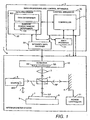
- Figure 1 shows a simplified schematic block diagram of apparatus 1 for determining surface characteristics, in particular the surface roughness ofathin film structure consisting of a substrate or base carrying one thin film layer or a stack of two or more thin film layers, where the surface roughness is the root mean square surface deviation corresponding to spatial wavelengths in excess of approximately 1 micrometre.
- a definition of surface roughness is to be found in ANSI standard B46.12002.
- thin film layer means a substantially transmissive film layer that is sufficiently thin to exhibit interference effects, in practice a film layer having a thickness in the region of 10s of nanometres to 100s of nanometres so that the mean thickness of the film is less than the coherence length of the light source where the interferometer is a focussed interferometer.
- the apparatus 1 has an interferometer system 2 and data processing and control apparatus 3.
- the interferometer system 2 is based on a conventional interferometer and may have a Mirau, Michelson or Linnik configuration, for example. Where the interferometer system is configured to carry out phase shifting interferometry, then the interferometer will have a monochromatic light source 4 whereas where the interferometer system 2 is configured to carry out coherence scanning interferometry, the interferometer will have a broadband source 4 which may be, for example, a white light source such as a quartz halogen lamp coupled to a regulated DC power supply having a light intensity output user control 400 provided, for example, in the form of a user-rotatable knob.
- a white light source such as a quartz halogen lamp coupled to a regulated DC power supply having a light intensity output user control 400 provided, for example, in the form of a user-rotatable knob.
- the source 4 provides light L which is split by abeam splitter (illustrated in Figure 1 as a single beam splitting prism) 5 into a first light beam which is directed along a reference path RP towards a reference mirror 6 and a second light beam which is directed along a sample path SP towards a surface 7 of a thin film structure 8 mounted on a sample support stage 9.
- abeam splitter illustrated in Figure 1 as a single beam splitting prism
- a focussing element 3 may be provided to focus an image of the region of interference onto a detector 10.
- the detector 10 has a 2D (two-dimensional) array SA of image sensing elements SE, one row of which is shown very diagrammatically in Figure 1 .
- the array SA images an area of the sample surface 7 falling within the field of view of the detector 10.
- Each individual sensing element SE of the 2D sensing array of the detector 10 detects the portion of the interference pattern falling within the acceptance cone of that element and resulting from a corresponding surface region or surface pixel of the area of the sample surface 7 so that, effectively, the imaged area of the surface can be considered as a 2D array of surface regions or surface pixels.
- the detector 10 is a CCD (Charge Coupled Device) digital camera, for example, a Vosskühler GmbH: CCD 1300 CCD digital camera.
- CMOS detector having a 2D (two-dimensional) xy array of CMOS sensing elements may be used.
- each of the sensing elements is square to provide the same resolution in both directions (x and y) of the array.
- a motion controller 11 is provided to effect relative movement between the thin film structure and the reference mirror 6 so as to change the difference between the lengths of the paths travelled by light reflected from the reference mirror 6 and light reflected from the sample surface 7. As shown in Figure 1 , the motion controller 11 is arranged to move the reference mirror 6 along the reference path RP. This is equivalent to moving the sample surface 7 along a scan path in the Z direction shown in Figure 1 .
- the detector 10 is arranged to capture or sense the light intensity (i.e. the interference pattern) at intervals as the path length difference between the thin film structure and the reference mirror 6 is changed.
- the motion controller will cause a number, generally four, of ⁇ /4 phase steps where ⁇ is the wavelength of the monochromatic light source and the detector will capture or sense the light intensity at each phase step.
- the motion controller will cause relative movement along a scan path and the detector will capture or sense the light intensity at intervals corresponding to axial changes in the relative position of the thin film structure of, for example, ⁇ /8, where ⁇ is the nominal central wavelength of the broadband source and the step may be for example 75nm.
- 2D image or frame data representing the intensity pattern for the field of view of the detector 10 is acquired by the detector 10 at each interval.
- the data processing and control apparatus 3 has control apparatus 30 for controlling operation of the interferometer system 2, an intensity data receiver 33 for receiving intensity data signals from the detector 10, a data processor 32 for processing the intensity data under the control of a controller 21 of the control apparatus 30 and a user interface 31 for enabling auser or operator: to control operation of apparatus; to be provided with a data output representing the results of processing by the data processor 32 of the data acquired during a measurement operation; and to enable messages such as error messages to be communicated to the user.
- the controller 21 of the control apparatus 30 controls overall operation of the apparatus and communicates with the user interface 31 and data processor 32.
- the dataprocessor 32 is operable to determine surface characteristics such as surface roughness of a thin film structure and to this end comprises a surface characteristic determiner 101 for determining the interfacial surface roughness and a gain determiner 100 for determining a gain value or values for use by the surface characteristic determiner 101 in determining the interfacial surface roughness, where the term "gain" means the rate of change of the apparent surface height with thin film thickness and represents the effect on the surface roughness measurements of the actual thin film structure being measured (for example the effect of refractive indices and film thicknesses) and the optical characteristics of the interferometer system.
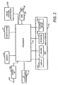
- At least the controller 21 and data processor 32 ofthe data processing and control apparatus may be implemented by programming computing apparatus, for example a personal computer.
- Figure 2 shows a simplified block diagram of such computing apparatus.
- the computing apparatus has a processor 25 associated with memory 26 (ROM and/or RAM), a mass storage device 27 such as a hard disk drive, a removable medium drive (RMD) 28 for receiving a removable medium (RM) 29 such as a floppy disk, CDROM, DVD or the like, input and output(I/O) controllers 37 for interfacing with the components of the broadband scanning interferometer system to be controlled by the control apparatus to enable the processor 25 to control operation of these components.
- ROM and/or RAM a processor 25 associated with memory 26 (ROM and/or RAM), a mass storage device 27 such as a hard disk drive, a removable medium drive (RMD) 28 for receiving a removable medium (RM) 29 such as a floppy disk, CDROM, DVD or the like
- I/O controllers 37 for interfacing with the components of the broadband scanning inter
- the user interface 31 consists, in this example, ofakeyboard 31 a, a pointing device 31b, a display such as a CRT or LCD display 36a and a printer 36b.
- the computing apparatus may also include a communications interface (COMMS INT) 199 such as a modem or network card that enables the computing apparatus to communicate with other computing apparatus over a network such as a local area network (LAN), wide area network (WAN), an Intranet or the Internet.
- COMMS INT communications interface
- the intensity data receiver 33 is provided as a dedicated frame capture circuit board 230 installed within the computing apparatus.
- the processor 25 may be programmed to provide the data processor 32 and controller 21 by any one or more of the following ways: 1) by pre-installing program instructions and any associated data in a non-volatile portion ofthe memory 26 or on the mass storage device 27; 2) by downloading program instructions and any associated data from a removable medium 29 received within the removable medium drive 28; 3) by downloading program instructions and any associated data as a signal SG supplied from another computing apparatus via the communications interface 199; and 4) by user input via the user interface 31.
- the thin film assembly may be evaluated in known manner.
- Abelè's matrix approach to the determination of electric field reflectance r may be used as described in, for example, sections 4.8 and 4.9 of" Optical Properties of Thin Solid Films" by O.S. Heavens published in 1991 (ISBN 0-486-66924-6 ).
- the electric field reflectance r of the thin film structure may be calculated by using the concept of optical admittance as described in, for example, sections 2.3, 2.4,2.5,2.6 and 2.7 of " Thin-Film Optical Filters" by H Angus Macleod (ISBN 0 7503 0688 2 ).
- Other approaches may also be possible.
- equation 2 the first two terms represent the phase terms corresponding to the geometrical perturbation and the last term represents the perturbation in the phase change on reflection.
- v o is the frequency of the wavelength ⁇ o of the monochromatic interferometer system
- G k is a gain value for the k th layer and represents the amount by which the actual z-perturbation dz k for the k th layer has to be multiplied
- the gain values G k correspond, for each thin film, to the rate of change of the apparent surface height with that thin film thickness and the gain values as a set represent the effect on the surface roughness measurements of the actual thin film structure being measured (for example the effect of refractive indices and film thicknesses) and the optical characteristics of the interferometer system, where the optical characteristics are, in this example, the interferometer wavelength and the numerical aperture.
- G k ⁇ O 4 ⁇ ⁇ . ⁇ ⁇ z k .
- the gain determiner 100 maybe configured to evaluate the gain G l (v o ) of the single thin film analytically. More generally, the gain determiner 100 will be configured to evaluate the gain values G k (v o ) by numerical differentiation.
- the gain determiner 100 will evaluate partial derivatives of equation 10 as follows: ⁇ Im r ⁇ z k ⁇ Im ⁇ r z k + ⁇ ⁇ z k - Im ⁇ r z k - ⁇ ⁇ z k 2 ⁇ ⁇ ⁇ z k and ⁇ Re r ⁇ z k ⁇ Re ⁇ r z k + ⁇ ⁇ z k - Re ⁇ r z k - ⁇ ⁇ z k 2 ⁇ ⁇ ⁇ z k
- ⁇ z k is a perturbation that represents a very small change in the physical thickness of the k th thin film layer with the value of ⁇ z k being the same for each thin film layer k.
- the gain determiner 100 obtains the electric field reflectances r zk of the k layers by taking advantage of the plane-wave angular spectrum approach discussed in " The distorted helix: Thin film extraction from scanning white light interferometry" by Daniel Mansfield published in the Proceedings ofSPIE Volume 6186, 618600,2006 at pages 1 to 11 where the original s and p field reflectances are evaluated using, for example, the standard matrix-based approach as presented in Chapter 2 of the aforementioned text book by Macleod using known or provided values for the substrate and thin film layer refractive indices and the respective nominal thickness of each ofthe thin film layers, that is the thicknesses specified by the designer of the thin film assembly.
- the gain determiner 100 determines the gain values G k in accordance with: 1 + 1 4 ⁇ ⁇ ⁇ ⁇ o ⁇ R ⁇ Re r ⁇ ⁇ Im r ⁇ z k - Im r ⁇ ⁇ Re r ⁇ z k
- the determined gain values are stored by the gain determiner 100.
- the surface characteristic determiner 101 prompts the user to cause the apparatus to make at least m+1 different measurements of apparent surface roughness Sq 2 app1 to Sq 2 appm+1 on m different thin film structure samples that differ from one another only in at least one of the thickness of one or more of the thin film layers and the number of thin film layers.
- the material forming the substrate and the materials and the sequence or order of thin film material layers will be the same for each sample, although the number of thin film layers and thicknesses differ between samples.
- the surface characteristic determiner 101 can solve equation 12b) for the substrate roughness Sq subs and for each of the root mean square thicknesses T 1 ,T 2 ,T 3 , .T m , because all the gain terms G 11 to G m+1 , m have been determined by the gain determiner 100.
- the m+1 different measurements of apparent surface roughness Sq 2 app1 to Sq 2 appm+1 are made on m different thin film structure samples.
- the m+1 measurements may be made on a single sample.
- the m+1 measurements comprise a first measurement of the apparent surface roughness of the uncoated substrate followed by successive measurements of the surface roughness of the thin film layers. This may be achieved by designing the thin film structure so that a measurement region of the substrate and each thin film layer is exposed in the final thin film structure or by making the measurements during manufacture so that the thin film layers are sequentially manufactured and then measured both in terms of apparent surface topography and in terms of mean layer thickness (by, for example, an ellipsometer), one layer at time.
- the surface characteristic determiner 101 may also evaluate the entire set of thickness departures( ⁇ z k ( x , y )) from the mean layer thicknesses together with the substrate local departure, ⁇ z subs ( x , y ) in accordance with: 1 0 0 ... 0 1 G 21 0 .... 0 1 G 31 G 32 0 .... .... .... .... .... 1 G m + 1 , 1 G m + 1 , 2 ....
- r * r 1 2 + r 2 2 + 2 ⁇ r 1 ⁇ r 2 cos 2 ⁇ ⁇ 1 1 + r 1 2 r 2 2 + 2 ⁇ r 1 ⁇ r 2 cos 2 ⁇ ⁇ 1
- Re r r 1 ⁇ 1 + r 2 2 ⁇ cos 2 ⁇ ⁇ 1 + r 2 ⁇ 1 + r 1 2 1 + r 1 2 ⁇ r 2 2 + 2 ⁇ r 1 ⁇ r 2 cos 2 ⁇ ⁇ 1
- Im r - r 1 ⁇ 1 - r 2 2 ⁇ sin 2 ⁇ ⁇ 1 1 + r 1 2 ⁇ r 2 2 + 2 ⁇ r 1 ⁇ r 2 cos 2 ⁇ ⁇ 1
- Figures 3 and 4 show flow charts for illustrating the operation of the apparatus in this case, that is where the apparatus shown in Figure 1 is configured as a low numerical aperture monochromatic interferometer and to carry out phase shifting interferometry where the sample comprises a thin film structure having a single thin film layer and the interfacial surface roughness to be determined is the thin film-ambient atmosphere (usually air) interface surface roughness.
- the apparatus shown in Figure 1 is configured as a low numerical aperture monochromatic interferometer and to carry out phase shifting interferometry where the sample comprises a thin film structure having a single thin film layer and the interfacial surface roughness to be determined is the thin film-ambient atmosphere (usually air) interface surface roughness.
- Figure 3 shows a flow chart illustrating one way in which the gain determiner 101 may determine the gain for a thin film structure having a single thin film.
- the gain determiner 100 first determines the operational wavelength ⁇ of the interferometer at S 1, the refractive indices of the substrate and the single thin film layer at S2 and the expected or specified mean thin film thickness of the single thin film layer at S3. It will of course be appreciated that the order in which these are determined is not important and that, for example, the thin film thickness could be determined first.
- the operational wavelength may be pre-stored by the apparatus or input by the user using the user interface 31 in response to a prompt issued via the user interface 31.
- the refractive index and mean film thickness will generally be input by the user using the user interface 31 in response to a prompt issued via the user interface 31.
- the refractive index may be determined by any appropriate conventional manner (for example, ellipsometry or spectrophotometry) or may be supplied by the manufacturer of the sample.
- the expected or specified mean thin film thickness may be determined by, for example, ellipsometry or spectrophotometry orby using the techniques described in WO2006/005959 or may be supplied by the manufacturer of the sample.
- the gain determiner 100 determines at S4 the surface electric field reflectance r by using the standard matrix relationship as discussed in the afore-mentioned text book by Macleod.
- the gain determiner 100 calculates the gain G 1 ( v o ) of the single thin film either analytically or by numerical differentiation as discussed above with respect to equations 10, 11a and 11b and 22.
- the gain G 1 is thus dependent upon the refractive index and mean thin film thickness of the single thin film plus the refractive index of the substrate and the measurement wavelength of the monochromatic light source.
- the mean thin film thickness of the single thin film is supplied by the user.
- the refractive indices may be supplied by the user or may be determined by the gain determiner 100 from information supplied by the user that identifies the materials forming the substrate and the layer and a data base (which may be local to the apparatus or may be accessed over a network or other communications link) of material refractive indices.
- the measurement wavelength of the monochromatic light source may be-pre-stored by the gain determiner 100 or provided by the controller 21.
- the gain G 1 is calculated at the time the user wishes to determine the surface roughness ofthe thin film structure.
- the gain determiner 100 or the controller 21 may store a look-up table or similar data set giving the calculated gain G 1 for different combinations of substrate refractive index, thin film refractive index and mean thin film thickness, in which case the gain determiner 100 will simply look-up rather than calculate the gain G 1 when the user inputs the refractive index and mean thin film thickness.
- the gain determiner 100 or the controller 21 may store a look-up table or similar data set giving the calculated gain G 1 for a number of different thicknesses of each of a number of specific thin film materials.
- the user may be prompted to input the mean thin film thickness and data identifying the material rather than the refractive index.
- the user will be prompted either to input the refractive index or to further identify the material.
- the gain determiner 100 calculates the gain as being approximately zero, then the gain determiner 100 will instruct the controller 21 to advise the user, via the user interface 31, that no gain compensation will be feasible because of the poor signal to noise ratio and, if a different measurement wavelength is available, will advise the user that the measurement wavelength should be changed to change the gain. If this is not possible then the controller 21 will advise the user via the user interface 31 that the interferometric measurement of the thin film sample should be abandoned.
- Figure 4 illustrates determination ofthe interfacial surface roughness for the single thin film thin film structure using the gain G 1 determined by the gain determiner 100.
- the surface characteristic determiner 101 determines avalue for the surface roughness Sq 2 subs of the substrate. Generally, this will be determined by prompting the user, via the user interface 31, to cause the sample support stage to be moved under the control of the control apparatus to bring a part ofthe sample free ofthe thin film into the field of view of the interferometer and then to instruct the control apparatus to carry out a measurement operation in which, for each surface pixel in the field ofview, the detector senses the light intensity at each of the number of phase steps and the surface characteristic determiner 101 then determines the phase and thus the surface height for each of those surface pixels in accordance with the usual phase shifting equations as set out in the above-mentioned sections of Optical Shop Testing by Daniel Malacara. The substrate surface roughness Sq 2 subs will then be determined as being the square ofthe deviation in z of the measured surface pixels.
- the surface characteristic determiner 101 determines the apparent surface roughness Sq 2 app for the single thin film of the thin film structure. Generally, this will be determined by prompting the user, via the user interface 31, to cause the sample support stage to be moved under the control of the control apparatus to bring a part of the sample carrying the thin film into the field of view of the interferometer and then to instruct the control apparatus to carry out a measurement operation in which, for each surface pixel in the field ofview, the detector senses the light intensity at each ofthe number of phase steps and the surface characteristic determiner 101 then determines the phase and thus the surface height z app for each of those surface pixels in accordance with the usual phase shifting equations or phase shifting algorithm as set out in above-mentioned sections of Optical Shop Testing by Daniel Malacara. The thin film surface roughness Sq 2 app will then be determined as being the square of the deviation in z of the measured surface pixels.
- the surface characteristic determiner 101 accesses the gain value G 1 determined by the gain determiner 100 and at S13 calculates the actual top surface roughness Sq 2 .
- the surface characteristic determiner 101 determines that the thin film RMS thickness is much greater (for example approximately three times greater) than the substrate surface roughness: T 1 ⁇ Sq subs then the surface characteristic determiner 101 decides that it is reasonable to carry out an approximate calculation to determine Sq as follows: Sq 2 ⁇ Sq app 2 / G 1 2 ⁇ o dz ⁇ dz app / G 1 ⁇ o
- Figure 5 shows the gain (G 1 ) determined by the gain determiner 100 for a number of sets A to K of thin film structures each of which consists of a single thin film on a substrate having a refractive index of 1.5.
- the refractive index of the thin films varies from 1.25 for set A to 2.5 for set K and within each set A to K the thin film optical thickness varies from zero to ⁇ /2 where ⁇ is the wavelength of the monochomatic source ofthe interferometer system.
- ⁇ is the wavelength of the monochomatic source ofthe interferometer system.
- Figure 6 shows the reflectance r as a function of film thickness for the same range of refractive indices (1.25 to 2.5) and a substrate refractive index of 1.5. At a quarter-wavelength thickness, the maximum reflectance is exhibited by the film of highest index.
- the above described operation of the gain determiner 100 and the surface characteristic determiner 101 is for a thin film structure having a single thin film layer.
- the apparatus may be configured to enable the interfacial surface roughness to be determined only for thin film structures having a single layer.
- the apparatus may be configured to enable the interfacial surface roughness to be determined for thin film structures having one or more thin film layers.
- the controller 21 will prompt the user to provide the number of thin film layers and the mean film thickness and refractive index for each thin film layer and will provide instructions to the user to enable measurements of the apparent surface roughness of each thin film in the thin film structure in addition to the measurement of the apparent surface roughness of the substrate.
- the user instead of provided the refractive index, the user provide information identifying the material so that the refractive index can be obtained from a data base accessible by the apparatus.
- the gain determiner will calculate gain values G k (v o ) for the thin film structure in accordance with equation 10 above while the surface characteristic determiner 101 will determine the interfacial surface roughness in accordance with equations 12 and 14 above.
- Gainvalues G k (v o ) calculated for thin film structures may be stored by the gain determiner 100 in association with the details of that thin film structure so that, if the gain determiner 100 determines that the thin film details entered by the user match those of a structure for which the gain values have already been calculated, recalculation is not necessary.
- the gain determiner 100 will carry out calculations in accordance with equation 10 to determine the gains G 11 , G 12 and G 22 and the controller 21 will advise the user to make measurements of the apparent surface roughness of the uncoated substrate (Sq subs ), the first layer only (Sq app (1)) and the surface of the two-film thin film structure ( Sq app (2)).
- Sq subs and Sq app (1) exposed parts of the substrate surface and first thin film layer need to be brought into the field of view of the interferometer. These measurements may, but need not necessarily, be made on the same sample.
- the measurements may be made on one, two or three samples, provided that the samples are produced by the same process using the same substrate material and the same thin film materials and material layer order.
- the thickness ofathin film on which a measurement is to be made may be selected so as to optimise the signal to noise ratio in the gain curve.
- those measurements may be used during the determination of the actual top surface roughness of other thin film structures produced from the same materials and using the same process conditions but which may have different thin film layer thicknesses so that it is not necessary to provide measurement access to each thin film layer surface in those other thin film structures.
- the surface characteristic determiner 101 may determine a value for the root mean square thickness of the or one of the thin film layer as an alterative to or in addition to the actual top surface roughness. Such a value may be used, for example, to determine whether the thin film assembly meets manufacturing quality control tolerances.
- the electrical field should be integrated over the numerical aperture for that objective to yield a net field reflectance to replace the electrical field reflectance r in equation 34. Otherwise the apparatus functions in the manner described above.
- Figure 7 shows a graph of gain G 1 against thickness in micrometres (um) for a silicon thin film on a silicon dioxide substrate where the interferometer system is configured for phase-shifting interferometry and has a measurement wavelength of 450nm (nanometres) and a x50 Mirau interference objective.
- the gain maxima occur at half wavelength locations.
- Figure 8 shows part of the graph of Figure 7 on an enlarged scale. Further results have show that increasing the measurement wavelength causes the gain maxima to decay more gradually with the gain maxima decay being far more gradual for a measurement wavelength of 600nm than for a measurement wavelength of 450nm.
- the thickness of the layers on which the surface roughness measurements are made may be selected to correspond to apeak in the corresponding gain curve so as to maximise the signal-to-noise ratio.
- the interferometer system is configured as a phase shifting interferometer system.
- the apparatus shown in Figure 1 may also be configured as a coherence scanning interferometer system. Further details of one example of a coherence scanning interferometer system 2 that may be used in the apparatus 1 will now be described with the aid of Figure 9 which shows an overall functional block diagram of the apparatus 1, Figure 10 which shows a simplified side elevational view of the interferometer system 2 and Figure 11 which shows a graph of intensity I against position Z to illustrate an example of the interference fringes (the axial interferogram) produced by coherence scanning interferometry for a sample surface pixel around a coherence peak or interference region.
- the coherence scanning interferometer system 2 is based on a Mirau type interferometer.
- an interferometer I of the broadband scanning interferometer system 2 has a broadband source 4 having first and second components 4' and 4" optically coupled by an optical fibre cable 4b.
- the first component 4' houses a quartz halogen projector bulb (with associated reflector).
- the second component comprises a series of optical elements through which light from the optical fibre cable 4b is transmitted.
- the series consists of a diffuses, a changeable filter, an aperture stop, a lens, a field stop and a collimating lens that provides an emergent light beam L.
- the filter may be a neutral density filter or a band pass filter, designed to restrict the wavelength range of the light emitted by the broadband source 4, such as a Helium-Neon laser line filter designed to pass light having a Helium-Neon laser line wavelength.
- the second component 4" of the broadband light source is arranged to supply broadband light L via a beam splitter 12 to an objective lens assembly 13 which includes, in addition to an objective lens 14, the beam splitter 5 and the reference mirror 6.
- the beam splitter 5 splits the light beam provided by the beam splitter 12 into a first reference beam that is directed along the reference path RP and a second sample beam that is directed along the sample path SP from the interferometer I towards the surface 7 of the thin film structure mounted on the sample support stage 9.
- Light returned to the beam splitter 12 is reflected towards the detector by the beam splitter and focussed onto the detector 10 by lens 3 (see Figure 1 ).
- the objective lens assembly 13, and thus the reference mirror 6, is movable in the Z direction by a Z direction mover 15, in this example a piezoelectric mover, under the control of servo/drive circuitry 15e of the control apparatus 30.
- the sample support stage 9 is movable in X and Y directions by anX mover 16 and a Y mover 17, respectively, to enable different areas ofthe sample surface 7 to be brought within the field of view of the detector 10.
- the majority F of the components of the interferometer I of the broadband scanning interferometer system 2 (apart from first component 4' of the light source and the optical fibre cable 4b) are provided within a housing 2a mounted via a carriage 18 to a Z axis datum column 19.
- the carriage 18 is coupled via a drive mechanism (not shown) such as a ball screw or lead screw drive mechanism to a coarse Z positioner 20 in the form of a manually operable control or, in this example, a DC motor that enables the carriage 18 and thus the interferometer I to be moved up and down the column 19 in the Z direction to enable the interferometer to be moved to different scanning start positions.
- the sample support stage 9 is provided on a support 102 which houses the X and Y movers 16 and 17.
- the X and Y movers 16 and 17 comprise, in this example, DC motors coupled to the sample support stage 9 by appropriate conventional drive mechanisms such as rack and pinion or ball screw drive mechanisms (not shown).
- each of the Z, X and Y movers is associated with a corresponding position sensor 15a, 16a and 17a while the coarse Z positioner 20 may be associated with a coarse Z positioner position sensor 20a.
- the dashed lines between the support stage 9 and the X and Y position sensors 16a and 17a in Figure 3 indicate that the position sensors may sense movement of the support stage 9 directly, rather than by signals derived from the corresponding motor.
- the controller 21 of the control apparatus 30 controls overall operation of the apparatus and communicates with the user interface 31 and data processor 32.
- the control apparatus 30 also include, in this example, the servo drive circuitry 15e and X, Y and Z loggers 22,23 and 24, each of which receives the output of the corresponding position sensor 16a,17a and 15a, and a trigger generator 60 for triggering operation of the detector 10 in response to the output of the Z position sensor 15a to capture images at the required intervals.
- the controller 21 also receives an output from the coarse Z positioner position sensor 20a, ifprovided.
- the controller 21 may be programmed in known manner to compensate for any error in the Z position due to the slight arcuate nature of the motion of the objective lens assembly 13.
- the intensity of the illumination sensed by one sensing element of the 2D sensing array (that is the portion of the interference pattern provided by light reflected from the corresponding surface region or surface pixel of the sample surface 7 imaged on that sensing element) varies as the path length difference changes with movement of the reference mirror 6, resulting in a series of fringes which have a coherence peak at the position along the scan path corresponding to zero path length difference.
- Figure 11 shows a graph of light intensity against position Z to illustrate the manner in which the intensity ofthe light sensed by a sensing element of the 2D sensing array of the detector 10 (and thus the interference fringe region) changes as the relative positions of the reference mirror 6 and sample surface 7 change.
- the envelope of the intensity distribution is the Fourier transform of the spectral distribution of the broadband source, modified by the spectral transmission of the instrument together with the spectral responsivity of the detector.
- the apparatus being described differs from that disclosed in WO03/078925 in the manner set out above with reference to Figure 1 , namely in that it is specifically intended for use in determining surface characteristics of a thin structure with a data processor providing in Figure 1 , a gain determiner 100 and a surface characteristic determiner 101.
- the gain determiner 100 will not calculate the gain in the manner described above because those calculations assume a single wavelength.
- the gain determiner 100 determines the gain values G k by modelling or simulating the performance of the coherence scanning interferometer system for the thin nim structure to be measured using data provided by the user for the thin film to be measured including the substrate complex refractive index and the complex refractive index (n-ik) and the thickness z k for each thin film of the thin film structure.
- z app + and z app - correspond respectively to the simulated interferometer z-response to having the k th thin film layer incremented and decremented by ⁇ z.
- I z j ⁇ Re F e i ⁇ 4 ⁇ ⁇ ⁇ ⁇ ⁇ z ⁇ ⁇ A R ⁇ ⁇ ⁇ A S ⁇ ⁇ ⁇ e i ⁇ ⁇ ⁇ ⁇
- I ( z ⁇ ) is the simulated interference intensity at the i th z location along the scan path
- a s ( v ) e i ⁇ ( v ) is obtained through taking advantage of the plane-wave angular spectrum approach discussed above where the original s and p field reflectances are evaluated using, say, the standard matrix-based approach as presented in Macleod, Thin-Film Optical Filters, the k th layer-thickness perturbation-induced term e i 4 ⁇ v ⁇ z is similarly obtained via the plane-wave angular spectrum
- this simulation takes the form of evaluating the net spectral electrical field reflectance, of then generating the corresponding axial-interferogram before finally subjecting this to the procedure described in WO03/078295 to extract the apparent surface height, z app . Perturbing the film thickness therefore gives direct access to G k through numerical differentiation.
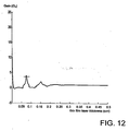
- Figure 12 shows a graph of gain against thin film thickness to illustrate an example of the gain data determined by the gain determiner 100 where the interferometer system comprises a coherence scanning interferometer system with a x50 Mirau objective lens assembly and where the thin film structure comprises a single thin film of silicon on a silicon dioxide substrate.
- the main effect of the broadband light source is to integrate out the gain maxima.
- the surface characteristic determiner 101 may determine the actual interfacial surface roughness in the manner described above for the case of the monochromatic phase shifting interferometer which requires the user to provide the thin film mean thickness(es).
- the surface characteristic determiner 101 may determine the thin film mean thickness(es) using the techniques described in WO2006/005959 , the whole contents of which are hereby incorporated by reference. Although this can be a relatively slow process, for a multilayer (or single layer) thin film it allows the thin film mean thickness(es) and mean geometric path length difference (which correspond to z) between the measurement and reference arms to be determined, provided that care is taken to ensure that the substrate and thin films are as flat as possible and are parallel to the reference mirror of the interferometer.
- the surface characteristic determiner 101 has the functionality of and carries out the operations of the layer structure determiner of WO2006/005959 and is operable to request the controller to prompt the user to input the dispersive refracfive index n base of the substrate and then to cause the apparatus to conduct in either order:1) a scan of a surface area of the substrate so that a set of intensity data is received by the intensity data receiver 33 for that surface area of the substrate for each scan interval along the scan path; and 2) a scan of a surface area of the surface of the thin film layer assembly so that a set of intensity data is received by the intensity data receiver 33 for that surface area of the layer structure for each scan interval along the scan path.
- the surface characteristic determiner 101 then carries out a frequency transformation process to provide frequency transformed intensity data for both the substrate and the thin film layer assembly intensity data.
- the frequency transformation is a Fourier transformation process and the frequency transformer is arranged to carry out a Fast Fourier Transform (FFT) procedure.
- FFT Fast Fourier Transform
- 2 n The well-known (2 n ) FFT may be used, although other forms of Fourier transform such as the Winograd Fourier transform (which is not based on powers of 2) could be used.
- the surface characteristic determiner 101 determines, under the control of the controller 21, the ratio between the positive frequency space sidebands of the Fourier transforms F ( I thin ( Z i )) SB + and F ( I base ( Z i )) SB + of the intensity data (if both transforms exceed a threshold, typically set at 5% of their maximum value) for the thin film layer assembly and the substrate, respectively, multiplied by a field reflectance term to provide a normalised HCF( ⁇ ) ratio.
- the field reflectance term consists of the difference between the dispersive refractive index of free space (set at 1) and the dispersive refractive index n base ( ⁇ ) of the substrate divided by the sum of the dispersive refractive index of free space and the dispersive refractive index of the substrate.
- the surface characteristic determiner 101 then requests the user to provide the number oflayers, approximate refractive indices and approximate thicknesses of the layers of thin film layer assembly together with an approximate or accurate value for the dispersive refractive index of the substrate and uses these in a thin film optimisation approach to extract the dispersive refractive index and thickness for each layer of the thin film layer assembly.
- the fitting procedure of the thin film optimisation approach may be, for example, a conjugate gradient method or a simulated annealing method as discussed in WO2006/005959 and as discussed in 'Numerical Recipes in Fortran: The Art of Scientific Computing, Second Edition' by William H. Press, Saul A. Teukolsky, William T. Vettering and Brian R. Flannery (ISBN 0-521-43064) in section 10.6 at pages 413 to 416 and section 10.9 at pages 436 to 438 .
- the local thickness of each layer (that is the thickness corresponding to a selected surface pixel or group of contiguous pixels) and its dispersive index is extracted by setting a ratio, the HCF ratio, related to the ratio between Fourier transforms ofthe intensity data (in the example described above the ratio of the positive frequency space sidebands ofthe Fourier Transforms) equal to an optical admittance ratio term that allows the use of thin film fitting procedures to extract the layer characteristics and that makes use of both the amplitude and the phase information available from the measurement operations.
- a ratio, the HCF ratio related to the ratio between Fourier transforms ofthe intensity data (in the example described above the ratio of the positive frequency space sidebands ofthe Fourier Transforms) equal to an optical admittance ratio term that allows the use of thin film fitting procedures to extract the layer characteristics and that makes use of both the amplitude and the phase information available from the measurement operations.
- the surface characteristic determiner 101 determines the HCF ratio or function in the manner discussed above and described in WO2006/005959 for a number of different locations within the field of view of the coherence scanning interferometer. The surface characteristic determiner 101 then determines a mean HCF function from the obtained HCF functions.
- the Taylor expansion of equation 46 above could be extended beyond the first order which would make the procedure more forgiving in the event of lack of flatness or tilt of the sample being measured.
- the surface characteristic determiner 101 repeats this procedure for other surface pixels within the field of view so generating the topography of each interface of the thin film structure, from which the surface roughness Sq can then be derived as discussed above by summing the individual layer topographies and the substrate topography.
- the gain determiner 100 calculates any of the gains as being approximately zero, then the gain determiner 100 will instruct the controller 21 to advise the user that no gain compensation will be feasible because of the poor signal to noise ratio and, if a different central measurement wavelength is available for the coherence scanning interferometer, will advise the user that the central measurement wavelength should be changed to change the gain. If this is not possible then the controller 21 will advise the user via the user interface 31 that interferometric measurement of the thin film sample should be abandoned.
- T j may be used for thin film structures comprising thin films of any reasonably transmissive materials that enable interference effects to be observed.
- the thin films will be dielectrics or semiconductors.
- possible thin film materials include titanium dioxide (TiO 2 ), tantalum oxide (Ta 2 O 5 ), silicon dioxide (SiO 2 ), Zirconium dioxide (ZrO 2 ), silicon.
- the present invention may be applied to forms of interferometry other than those discussed above.
- the spectral range of light source is in the visible. It could, however, extend into or lie within the infra red or ultra violet regions of the spectrum.
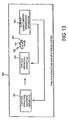
- FIG. 13 shows a simple block diagram of a thin film manufacturing system 400 comprising thin film designing apparatus 401 that comprises, generally, computing apparatus similar to that shown in Figure 2 programmed: to receive input from a user or operator identifying the features required of the thin film structure such as the required base or substrate, the materials to be used to form the thin film structure, the number of thin film layers and for example the optical characteristics (such as the optical admittance) required of the thin film structure; and to design a thin film structure consisting of layers of the user selected materials having thicknesses that provide the required optical characteristic following, for example, the teaching of the afore-mentioned text book " Thin- Film Optical Filters" by H Angus Macleod (ISBN 0 7503 0688 2 ).
- the thin film designing apparatus 401 provides control instructions for enabling a thin film deposition apparatus 402 to cause the required thin film layer structure to be produced.
- the tin film deposition apparatus 402 may be configured to form thin film layer(s) 405 on the base or substrate 406 using any known thin film deposition technique(s) such as sputtering, Low Pressure Chemical Vapour Deposition (LPCVD), Metal Organic Vapour Deposition (MOCVD), Molecular Beam Epitaxy (MBE) and so on.
- LPCVD Low Pressure Chemical Vapour Deposition
- MOCVD Metal Organic Vapour Deposition
- MBE Molecular Beam Epitaxy
- the resulting thin film structure 404 is passed to a surface characteristic determining apparatus 403 which is constructed and operates as described above to determine a surface characteristic or characteristics of a produced thin film structure.
- the surface characteristic determining apparatus 403 may provide control information for at least one of the thin film designing apparatus 401 and the thin film designing apparatus 401 to enable the designing and/or manufacturing process to be modified in accordance with the surface characteristic or characteristics determined by the surface characteristic determining apparatus 403.
Landscapes
- Physics & Mathematics (AREA)
- General Physics & Mathematics (AREA)
- Engineering & Computer Science (AREA)
- Signal Processing (AREA)
- Mathematical Physics (AREA)
- Length Measuring Devices By Optical Means (AREA)
Claims (34)
- Datenverarbeitungseinrichtung zum Empfangen, von einem Interferometer, erster Intensitätsdaten, die eine erste Gruppe von Intensitätswerten umfassen, und zweiter Intensitätsdaten, wobei die zweiten Intensitätsdaten zumindest eine zweite Gruppe von Intensitätswerten aufweisen, die von einem Messvorgang auf einem Oberflächenbereich einer Dünnfilmstruktur auf einem Substrat herrühren, und die erste Gruppe von Intensitätswerten von einem Messvorgang auf einem Oberflächenbereich des Substrats ohne eine Dünnfilmstruktur herrührt, wobei die Einrichtung aufweist:eine Verstärkungsbestimmungsvorrichtung, die dazu funktionsfähig ist, eine Verstärkung für den oder jeden Dünnfilm der Dünnfilmstruktur zu bestimmen; undeine Oberflächeneigenschafts-Bestimmungsvorrichtung, die dazu funktionsfähig ist, eine topografische Eigenschaft der Substratoberfläche auf der Grundlage der ersten Intensitätsdaten zu bestimmen, eine anscheinende topografische Eigenschaft der Dünnfilmstrukturoberfläche auf der Grundlage der zweiten Intensitätsdaten zu bestimmen, und die anscheinende topografische Eigenschaft der Dünnfilmstrukturoberfläche zu modifizieren, unter Verwendung der topografischen Eigenschaft der Substratoberfläche und der Verstärkung oder der Verstärkungen, die von der Verstärkungsbestimmungsvorrichtung bestimmt wird bzw. werden, wobei die Verstärkung die Änderungsrate der anscheinenden Oberflächenhöhe in Abhängigkeit von der Dicke des Dünnfilms repräsentiert.
- Einrichtung zur Bestimmung von Information in Bezug auf eine Oberflächeneigenschaft einer Probe in Form einer Dünnfilmstruktur, welche eine oder mehrere Dünnfilmschichten auf einem Substrat aufweist, wobei die Einrichtung aufweist:eine Datenverarbeitungseinrichtung nach Anspruch 1;eine Lichtquelle;einen Lichtdirektor, der dazu funktionsfähig ist, Licht von der Lichtquelle entlang einem Probenweg zu einem Oberflächenbereich der Probe zu richten, und entlang einem Bezugsweg zu einer Bezugsoberfläche, so dass Licht, das von dem Probenoberflächenbereich reflektiert wird, mit Licht interferiert, das von der Bezugsoberfläche reflektiert wird;eine Bewegungsvorrichtung, die dazu funktionsfähig ist, eine Relativbewegung entlang einem Messweg zwischen einer Probe und der Bezugsoberfläche zu bewirken;ein Erfassungsgerät, das dazu funktionsfähig ist, Licht zu erfassen, welches die Interferenzstreifen repräsentiert, die durch den Probenoberflächenbereich erzeugt werden; undeine Steuerung, die dazu funktionsfähig ist, einen Messvorgang durchzuführen, durch Veranlassen des Erfassungsgeräts, die Lichtintensität an einer Anzahl von Orten entlang dem Messweg zu erfassen, um für jeden Ort einen entsprechenden Intensitätswert zur Verfügung zu stellen.
- Einrichtung nach Anspruch 2, bei welcher die Lichtquelle eine monochromatische Lichtquelle ist, und die Verstärkungsbestimmungsvorrichtung dazu funktionsfähig ist, die Verstärkung für eine Dünnfilmschicht zu bestimmen, durch Bestimmung eines Wertes für den Brechungsindex und die mittlere Dicke des Dünnfilms der Dünnfilmschicht, Berechnung eines Oberflächenreflexionsgrades, und Verwendung des Oberflächenreflexionsgrades und des Brechungsindex zur Berechnung der Verstärkung.
- Einrichtung nach Anspruch 2 oder 3, bei welcher die Lichtquelle eine monochromatische Lichtquelle ist, und die Verstärkungsbestimmungsvorrichtung dazu funktionsfähig ist, die Verstärkung folgendermaßen zu bestimmen:

wobei dzapp eine Änderung oder Störung bei der anscheinenden Oberflächenhöhe ist, dzsubs eine Änderung oder Störung bei der Oberflächenrauhigkeit ist, dzk eine Änderung oder Störung bei der Oberflächenhöhe der k-ten Dünnfilmschicht ist, r die Reflexionsgradamplitude des elektrischen Feldes ist, R die Reflexionsgradintensität des elektrischen Feldes ist, und ν0 die Frequenz von λ0 der Lichtquelle ist. - Einrichtung nach Anspruch 2 oder 3, bei welcher die Lichtquelle eine monochromatische Lichtquelle ist, und, wenn die Dünnfilmstruktur einen einzigen Dünnfilm aufweist, die Verstärkungsbestimmungsvorrichtung dazu funktionsfähig ist, die Verstärkung folgendermaßen zu bestimmen:

wobei R die Reflexionsgradintensität des elektrischen Feldes ist, r die Reflexionsgradamplitude des elektrischen Feldes ist, und zk die Oberflächenhöhe des k-ten Dünnfilms ist. - Einrichtung nach Anspruch 2 oder 3, bei welcher die Lichtquelle eine monochromatische Lichtquelle ist, und, wenn die Dünnfilmstruktur einen einzigen Dünnfilm aufweist, die Verstärkungsbestimmungsvorrichtung dazu funktionsfähig ist, die Verstärkung folgendermaßen zu bestimmen:


wobei δ1 und z1 jeweils die Phase bzw. die physikalische Dicke des Dünnfilms ist, R die Reflexionsgradintensität des elektrischen Feldes ist, und r1 und r2 der Reflexionsgrad des elektrischen Feldes an der Film/Substrat-Grenzfläche bzw. der Luft/Dünnfilm-Grenzfläche ist. - Einrichtung nach einem der Ansprüche 2 bis 6, welche ein Interferometersystem aufweist, das ein Fokussierobjektiv aufweist, und bei welcher die Verstärkungsbestimmungsvorrichtung dazu funktionsfähig ist, die Verstärkung dadurch zu bestimmen, dass der Oberflächenreflexionsgrad durch einen Netto-Feldreflexionsgrad ersetzt wird, der durch Integrieren über die numerische Apertur des Objektivs bestimmt wird.
- Einrichtung nach einem der Ansprüche 2 bis 7, bei welcher die Steuerung dazu funktionsfähig ist, zu verursachen, dass die Orte auf dem Messweg um eine vorbestimmte Phase beabstandet sind, und die Oberflächeneigenschafts-Bestimmungsvorrichtung dazu funktionsfähig ist, eine Oberflächenhöhe eines Oberflächenpixels unter Verwendung eines Phasenverschiebungs-Algorithmus zu bestimmen.
- Einrichtung nach jedem voranstehenden Anspruch, bei welcher die Verstärkung für den Dünnfilm oder den k-ten Dünnfilm einer Dünnfilmstruktur gegeben ist durch:

wobei cosθ gleich 1 für eine niedrige numerische Apertur ist, λ0 die nominelle Zentrumswellenlänge der Lichtquelle ist, ϕ ein gemessner Phasenwinkel ist, und zk die Oberflächenhöhe des k-ten Dünnfilms ist. - Einrichtung nach einem der voranstehenden Ansprüche bei welcher die Verstärkungsbestimmungsvorrichtung dazu funktionsfähig ist, die Verstärkung für eine Dünnfilmschicht durch Bestimmung eines Wertes für den Brechungsindex und einer mittleren Dünnfilmdicke der Dünnfilmschicht, Berechnung eines Oberflächenreflexionsgrades, und Verwendung des Oberflächenreflexionsgrades und des Brechungsindex zur Berechnung der Verstärkung zu bestimmen.
- Einrichtung nach einem der voranstehenden Ansprüche, bei welcher die Oberflächeneigenschafts-Bestimmungsvorrichtung dazu funktionsfähig ist, die Oberflächenrauhigkeit zu bestimmen.
- Einrichtung nach einem der Ansprüche 1 bis 8, bei welcher die Oberflächeneigenschafts-Bestimmungsvorrichtung dazu funktionsfähig ist, die Oberflächenrauhigkeit Sq2 folgendermaßen zu bestimmen:

und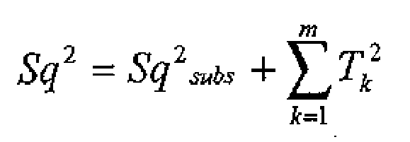
wobei Sq2 app die anscheinende Substratoberflächenrauhigkeit ist, Sq2 subs die tatsächliche Substratrauhigkeit ist, und Tk der quadratische Mittelwert der Dicke der k-ten Schicht einer Dünnfilmstruktur ist, welche m Schichten aufweist. - Einrichtung nach einem der Ansprüche 1 bis 11, bei welcher, wenn die Dünnfilmstruktur einen einzigen Dünnfilm mit einer Oberflächenrauhigkeit aufweist, die erheblich größer ist als jene des Substrats, die Oberflächeneigenschafts-Bestimmungsvorrichtung dazu funktionsfähig ist, die Oberflächenrauhigkeit Sq2 folgendermaßen zu bestimmen:

wobei Sq2 app die anscheinende Substratoberflächenrauhigkeit ist, und G1 die Verstärkung für den Dünnfilm ist. - Einrichtung nach Anspruch 2, bei welcher die Lichtquelle eine monochromatische Lichtquelle ist, die Dünnfilmstruktur zwei Dünnfilme aufweist, und die Verstärkungsbestimmungsvorrichtung dazu funktionsfähig ist, die Oberflächenrauhigkeit Sq2 folgendermaßen zu bestimmen:

wobei T1 und T2 der quadratische Mittelwert der Dicke der ersten bzw. der zweiten Schicht ist, G11 die Verstärkung für die erste Dünnfilmschicht in Abwesenheit der zweiten Dünnfilmschicht ist, G12 die Verstärkung für die erste Dünnfilmschicht ist, nachdem die zweite Dünnfilmschicht oben auf der ersten zur Verfügung gestellt wurde, und G22 die Verstärkung der zweiten Schicht ist. - Einrichtung nach Anspruch 2, bei welcher die Lichtquelle eine Breitband-Lichtquelle ist, die Steuerung dazu funktionsfähig ist, einen Messvorgang dadurch durchzuführen, dass das Erfassungsgerät dazu veranlasst wird, die Lichtintensität entlang einer Anzahl an Orten entlang dem Messweg zu erfassen, um für einen Oberflächenbereich eine Gruppe von Intensitätswerten zur Verfügung zu stellen, die ein Interferogramm in der Messwegrichtung repräsentieren, und der Datenprozessor dazu funktionsfähig ist, eine Oberflächenhöhe des Oberflächenbereichs zu bestimmen, durch Bestimmung der Position eines Kohärenzpeaks in den Intensitätswerten für diesen Oberflächenbereich.
- Einrichtung nach Anspruch 15, bei welcher die Verstärkung gegeben ist durch:

wobei zapp eine anscheinende Oberflächenhöhe ist, und zk eine tatsächliche Oberflächenhöhe ist. - Einrichtung nach Anspruch 15, bei welcher die Verstärkungsbestimmungsvorrichtung dazu funktionsfähig ist, einen Verstärkungswert für eine Dünnfilmschicht zu bestimmen, durch Bewertung eines Netto-Spektralreflexionsgrades für die Dünnfilmstruktur unter Verwendung von Werten zk für die Schichtdicken, Verwendung des bewerteten Netto-Spektralreflexionsgrades zur Erzeugung eines entsprechenden Interferogramms, Bestimmung der Position entlang dem Messweg des Kohärenzpeaks in dem Interferogramm, um eine anscheinende Schichtdicke zapp zu erhalten, Stören der Schichtdickenwerte zk um δzk, um die entsprechende Änderung δzapp zu bestimmen, in der anscheinenden Schichtdicke, und Bestimmung der Verstärkung Gk auf folgender Grundlage:

wobei zapp eine anscheinende Oberflächenhöhe ist, und zk eine tatsächliche Oberflächenhöhe ist. - Einrichtung nach Anspruch 17, bei welcher die Oberflächeneigenschafts-Bestimmungsvorrichtung dazu funktionsfähig ist, die Oberflächenrauhigkeit zu bestimmen.
- Einrichtung nach Anspruch 15 oder 16, bei welcher die Oberflächeneigenschafts-Bestimmungsvorrichtung dazu funktionsfähig ist, die Oberflächenrauhigkeit Sq2 folgendermaßen zu bestimmen:

und
wobei Sq2 app die anscheinende Substratoberflächenrauhigkeit ist, Sq2 subs die tatsächliche Substratrauhigkeit ist, und Tk der quadratische Mittelwert der Dicke der k-ten Schicht einer Dünnfilmstruktur mit m Schichten ist. - Einrichtung nach Anspruch 17, bei welcher, wenn eine Dünnfilmstruktur einen einzigen Dünnfilm mit einer Oberflächenrauhigkeit aufweist, die erheblich größer ist als jene des Substrats, die Oberflächeneigenschafts-Bestimmungsvorrichtung dazu funktionsfähig ist, die Oberflächenrauhigkeit folgendermaßen zu bestimmen:

wobei Sq2 app die anscheinende Substratoberflächenrauhigkeit ist, und G1 die Verstärkung für den Dünnfilm ist. - Einrichtung nach einem der Ansprüche 17 bis 20, bei welcher die Oberflächeneigenschafts-Bestimmungsvorrichtung dazu funktionsfähig ist, die Bestimmung einer Oberflächeneigenschaft zu ermöglichen, zur Bestimmung der mittleren Dicke bzw. der mittleren Dicken eines Dünnfilms bzw. von Dünnfilmen, und zwar folgendermaßen:Bestimmen eines Frequenztransformationsverhältnisses entsprechend einem Verhältnis zwischen ersten Intensitätsdaten, die eine erste Gruppe von Intensitätswerten aufweisen, die von einem Messvorgang auf einem Oberflächenbereich einer Dünnfilmschichtstruktur herrühren, und zweiten Intensitätsdaten, welche eine zweite Gruppe von Intensitätsdaten aufweisen, die von einem Messvorgang auf einem Oberflächenbereich des Substrats herrühren; undDurchführen eines Fits eines Schichtstrukturmodells, welches variable Modellparameter aufweist, die in Beziehung zu den Schichtdicken und Brechungsindices der Schichten der Dünnfilmstruktur stehen, an das Verhältnis, das durch die Verhältnisbestimmungsvorrichtung bestimmt wird, durch Einstellung der Modellparameter, um hierdurch für die Modellparameter Werte zu erhalten, welche die Schichtdicken und Brechungsindices der Schichten der Dünnfilmstruktur repräsentieren.
- Einrichtung nach Anspruch 17, bei welcher, um die Bestimmung der Oberflächenrauhigkeit zu ermöglichen, die Oberflächeneigenschafts-Bestimmungsvorrichtung dazu funktionsfähig ist, die mittlere Dicke bzw. die mittleren Dicken des Dünnfilms bzw. der Dünnfilme folgendermaßen zu bestimmen:Bestimmen eines Frequenztransformationsverhältnisses HCF entsprechend einem Verhältnis zwischen ersten Intensitätsdaten, welche eine erste Gruppe von Intensitätswerten aufweisen, die von einem Messvorgang auf einem Oberflächenbereich einer Dünnfilmschichtstruktur herrühren, und zweiten Intensitätsdaten, welche eine zweite Gruppe von Intensitätswerten aufweisen, die von einem Messvorgang auf einem Oberflächenbereich des Substrats herrühren; undDurchführen eines Fits mit einem Schichtstrukturmodell, welches variable Modellparameter aufweist, die in Beziehung zu den Schichtdicken und den Brechungsindices der Schichten einer Dünnfilmstruktur stehen, an das Verhältnis, das durch die Verhältnisbestimmungsvorrichtung bestimmt wurde, durch Einstellung der Modellparameter, wodurch für die Modellparameter Werte erhalten werden, welche die Schichtdicken und Brechungsindices der Schichten der Dünnfilmstruktur repräsentieren; undwobei die Oberflächeneigenschafts-Bestimmungsvorrichtung dazu funktionsfähig ist, die Oberflächenrauhigkeit zu bestimmen, durch Bestimmen eines Mittelwerts der Frequenztransformationsverhältnisse für eine Anzahl unterschiedlicher Oberflächenbereiche der Dünnfilmstruktur, und Bestimmung des Differentials des mittleren Frequenztransformationsverhältnisses
auf folgender Grundlage: wobei dzsubs eine Änderung oder Störung bei der Oberflächenrauhigkeit ist, und nachfolgendes Durchführen eines Fit-Vorgangs zur Bestimmung von dzsubs und dzk.
 - Einrichtung nach Anspruch 21 oder 22, bei welcher die Oberflächeneigenschafts-Bestimmungsvorrichtung dazu funktionsfähig ist, erste bezüglich der Frequenz transformierte Daten entsprechend den ersten Intensitätsdaten sowie zweite bezüglich der Frequenz transformierte Daten entsprechend den zweiten Intensitätsdaten zu bestimmen, und das Frequenztransformationsverhältnis zu bestimmen, durch Teilen entweder der ersten oder der zweiten bezüglich der Frequenz transformierten Daten durch die zweiten bzw. ersten bezüglich der Frequenz transformierten Daten und durch Multiplizieren dieses Verhältnisses mit einem Feldreflexionsgradterm:

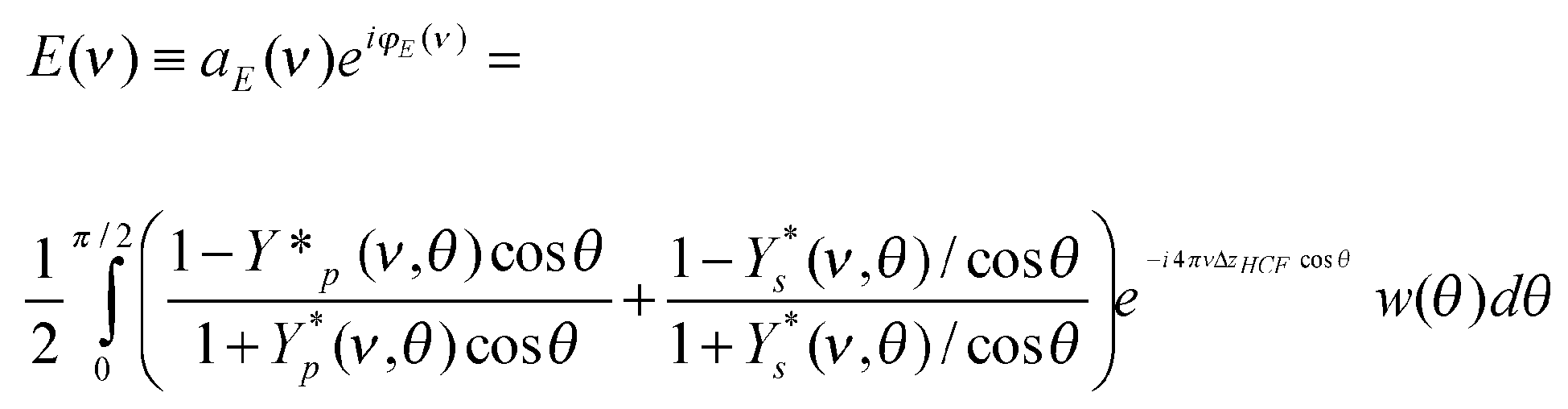
wobei nbase (v) der Brechungsindex bei der Frequenz ν des Substrats ist, und + entweder das Verhältnis oder dessen komplex Konjugierte angibt, und I(zi) eine simulierte Interferenzintensität an einem i-ten Z-Ort ist, und der Index SB+ das positive Frequenzseitenband der Fourier-Transformation bezeichnet. - Einrichtung nach Anspruch 21, 22 oder 23, bei welcher die Oberflächeneigenschafts-Bestimmungsvorrichtung dazu funktionsfähig ist, ein optisches Admittanzverhältnis E(v) zu bestimmen, gegeben durch:

wobei HFC(v) ein Frequenztransformationsverhältnis ist, w(θ) eine winkelabhängige Gewichtungsfunktion, bei welcher θ der Winkel ist, welcher der numerischen Apertur der Einrichtung zugeordnet ist, aHFC die HFC-Amplitude ist, der Exponent der HFC-Phasenterm ist, und der Feldreflexionsgradterm Terme für Felder mit s- und p-Polarisation enthält, wobei η ein Brechungsindex ist, und I(zi) eine simulierte Interferenzintensität an einem i-ten z-Ort ist. - Einrichtung nach einem der Ansprüche 21 bis 24, bei welcher das Schichtstrukturmodell ein Modell für die optischen Admittanz einer Dünnfilmschichtstruktur ist.
- Einrichtung nach einem der Ansprüche 20 bis 24, bei welcher das Schichtstrukturmodell ein Modell für die optische Admittanz einer Dünnfilmschichtstruktur wie folgt ist:

wobei Y+ die optische Admittanz bezeichnet, oder deren komplex Konjugierte, und der Exponent ein helixförmiger Phasenterm ist. - Einrichtung nach einem der Ansprüche 21 bis 24, bei welcher das Schichtstrukturmodell ein Modell für die optische Admittanz einer Dünnfilmschichtstruktur wie folgt ist:
wobei Y*p und Y*s die komplex Konjugierte der optischen Admittanz in der p- bzw. s-Ebene der Polarisation sind. - Einrichtung nach Anspruch 16 oder 17, bei welcher, um eine Bestimmung der Oberflächenrauhigkeit zu ermöglichen, die Oberflächeneigenschafts-Bestimmungsvorrichtung dazu funktionsfähig ist, eine oder mehrere Dünnfilmdicken folgendermaßen zu bestimmen:Bestimmen eines Frequenztransformationsverhältnisses entsprechend einem Verhältnis zwischen ersten Intensitätsdaten, die eine erste Gruppe von Intensitätswerten aufweisen, die von einem Messvorgang auf einem Oberflächenbereich einer Dünnfilmschichtstruktur herrühren, und zweiten Intensitätsdaten, die eine zweite Gruppe von Intensitätswerten aufweisen, die von einem Messvorgang auf einem Oberflächenbereich des Substrats herrühren, undDurchführen eines Fits eines Schichtstrukturmodells, welches variable Modellparameter aufweist, die in Beziehung zu den Schichtdicken von Brechungsindices der Schichten der Dünnfilmstruktur stehen, an das Verhältnis, das durch die Verhältnis-Bestimmungsbestimmungsvorrichtung bestimmt wird, durch Einstellung der Modellparameter, wodurch für die Modellparameter Werte erhalten werden, welche die Schichtdicken und die Brechungsindices der Schichten der Dünnfilmstruktur repräsentieren; undwobei die Oberflächeneigenschafts-Bestimmungsvorrichtung dazu funktionsfähig ist, die Oberflächenrauhigkeit zu bestimmen, durch Bestimmung eines Mittelwerts der Frequenztransformationsverhältnisse für eine Anzahl unterschiedlicher Oberflächenbereiche der Dünnfilmstruktur, und Modellieren des Frequenztransformationsverhältnisses für jeden Oberflächenbereich als eine Störung gegenüber dem mittleren Frequenztransformationsverhältnis, und nachfolgendes Durchführen eines Fit-Vorgangs zur Bestimmung von dzsubs und dzk.
- Einrichtung nach Anspruch 28, bei welcher das Frequenztransformationsverhältnis ein Produkt des Reflexionsgrades des elektrischen Feldes und eines Phasenvoreilungsfaktors für jeden Oberflächenbereich aufweist.
- Verfahren zur Bestimmung von Information in Bezug auf eine Oberflächeneigenschaft einer Probe in Form einer Dünnfilmstruktur, die eine oder mehrere Dünnfilmschichten auf einem Substrat aufweist, wobei das Verfahren umfasst:Richten von Licht von einer Lichtquelle entlang einem Probenweg zu einem Oberflächenbereich der Probe, und entlang einem Bezugsweg zu einer Bezugsoberfläche, so dass Licht, das von dem Probenoberflächenbereich reflektiert wird, und Licht interferieren, das von der Bezugsoberfläche reflektiert wird;Durchführen einer Relativbewegung entlang einem Messweg zwischen der Probe und der Bezugsoberfläche;Durchführen eines Messvorgangs dadurch, dass das Erfassungsgerät zum Erfassen von Licht an einer Anzahl von Orten entlang dem Messweg veranlasst wird, um für jeden Ort einen entsprechenden Intensitätswert zur Verfügung zu stellen; undVerarbeiten von Intensitätsdaten, welche eine erste Gruppe von Intensitätswerten und zweiten Intensitätsdaten aufweisen, wobei die zweiten Intensitätsdaten zumindest eine zweite Gruppe von Intensitätswerten aufweisen, die von einem Messvorgang auf einem Oberflächenbereich der Dünnfilmstruktur auf dem Substrat herrühren, und die erste Gruppe von Intensitätswerten von einem Messvorgang auf einem Oberflächenbereich des Substrats ohne eine Dünnfilmstruktur herrührt, wobei die Verarbeitung umfasst, eine anscheinende topografische Eigenschaft der Substratoberfläche auf der Grundlage der ersten Intensitätsdaten zu bestimmen, eine anscheinende topografische Eigenschaft der Dünnfilmstrukturoberfläche auf der Grundlage der zweiten Intensitätsdaten zu bestimmen, und die anscheinende topografische Eigenschaft der Dünnfilmstrukturoberfläche zu modifizieren, unter Verwendung der anscheinenden topografischen Eigenschaft der Substratoberfläche und einer bestimmten Verstärkung oder mehreren bestimmten Verstärkungen, wobei die Verstärkung die Änderungsrate der anscheinenden Oberflächenhöhe in Abhängigkeit von der Dünnfilmdicke repräsentiert.
- Computerprogramm, welches Programmbefehle zum Programmieren der Datenverarbeitungseinrichtung der Einrichtung nach Anspruch 2 aufweist, um die Verarbeitungsschritte eines Verfahrens gemäß Anspruch 30 durchzuführen.
- Computerprogramm nach Anspruch 31, welches Programmbefehle zum Programmieren der Datenverarbeitungseinrichtung der Einrichtung nach Anspruch 2 aufweist, um die Steuerung zum Steuern der Einrichtung nach Anspruch 2 bereitzustellen, um den Relativbewegungsschritt und den Messschritt von Anspruch 30 durchzuführen.
- Speichermedium, welches Programmbefehle zum Programmieren der Datenverarbeitungseinrichtung der Einrichtung nach Anspruch 2 aufweist, um die Verarbeitungsschritte eines Verfahrens gemäß Anspruch 30 durchzuführen.
- Speichermedium nach Anspruch 33, welches Programmbefehle zum Programmieren der Datenverarbeitungseinrichtung der Einrichtung nach Anspruch 2 aufweist, um die Steuerung zum Steuern der Einrichtung nach Anspruch 2 zur Verfügung zu stellen, um den Relativbewegungsschritt und den Messschritt des Anspruchs 30 durchzuführen.
Applications Claiming Priority (3)
| Application Number | Priority Date | Filing Date | Title |
|---|---|---|---|
| GB0526228A GB0526228D0 (en) | 2005-12-22 | 2005-12-22 | Interfacial surface roughness measurement using SWLI |
| GB0614358A GB2440164A (en) | 2006-07-19 | 2006-07-19 | Apparatus for and a method of determining surface characteristics |
| PCT/GB2006/004714 WO2007071944A1 (en) | 2005-12-22 | 2006-12-15 | Apparatus for and a method of determining surface characteristics |
Publications (2)
| Publication Number | Publication Date |
|---|---|
| EP1963780A1 EP1963780A1 (de) | 2008-09-03 |
| EP1963780B1 true EP1963780B1 (de) | 2012-02-08 |
Family
ID=37865711
Family Applications (1)
| Application Number | Title | Priority Date | Filing Date |
|---|---|---|---|
| EP06820549A Not-in-force EP1963780B1 (de) | 2005-12-22 | 2006-12-15 | Vorrichtung und verfahren zur bestimmung von oberflächeneigenschaften |
Country Status (4)
| Country | Link |
|---|---|
| US (2) | US8112246B2 (de) |
| EP (1) | EP1963780B1 (de) |
| AT (1) | ATE545002T1 (de) |
| WO (1) | WO2007071944A1 (de) |
Cited By (1)
| Publication number | Priority date | Publication date | Assignee | Title |
|---|---|---|---|---|
| CN104613882A (zh) * | 2015-02-12 | 2015-05-13 | 江苏宇迪光学股份有限公司 | 一种基于光学相位解调的透镜中心厚度测量装置及利用其的测量方法 |
Families Citing this family (15)
| Publication number | Priority date | Publication date | Assignee | Title |
|---|---|---|---|---|
| WO2008124868A1 (en) * | 2007-04-13 | 2008-10-23 | Renewable Energy Systems Limited | Power generation and energy recovery systems and methods |
| US8120781B2 (en) * | 2008-11-26 | 2012-02-21 | Zygo Corporation | Interferometric systems and methods featuring spectral analysis of unevenly sampled data |
| US9086483B2 (en) * | 2011-03-28 | 2015-07-21 | Northrop Grumman Guidance And Electronics Company, Inc. | Systems and methods for detecting and/or identifying materials |
| US9696138B2 (en) * | 2011-08-01 | 2017-07-04 | University Of Florida Research Foundation, Inc. | Simultaneous refractive index and thickness measurements with a monochromatic low-coherence interferometer |
| JP5901305B2 (ja) * | 2011-08-02 | 2016-04-06 | 東京エレクトロン株式会社 | 光干渉システム、基板処理装置及び測定方法 |
| WO2013028196A1 (en) | 2011-08-25 | 2013-02-28 | Alliance For Sustainable Energy, Llc | On-line, continuous monitoring in solar cell and fuel cell manufacturing using spectral reflectance imaging |
| NL2009273A (en) * | 2011-08-31 | 2013-03-04 | Asml Netherlands Bv | Level sensor arrangement for lithographic apparatus, lithographic apparatus and device manufacturing method. |
| GB2497098B (en) * | 2011-11-30 | 2018-01-03 | Taylor Hobson Ltd | Metrological apparatus and a method of determining a surface characteristic or characteristics |
| US20130226330A1 (en) * | 2012-02-24 | 2013-08-29 | Alliance For Sustainable Energy, Llc | Optical techniques for monitoring continuous manufacturing of proton exchange membrane fuel cell components |
| US10254110B2 (en) * | 2013-12-18 | 2019-04-09 | Nanometrics Incorporated | Via characterization for BCD and depth metrology |
| GB2529251A (en) * | 2014-08-15 | 2016-02-17 | Taylor Hobson Ltd | Apparatus for and a method of determining a characteristic of a sample |
| CN104297260B (zh) | 2014-11-04 | 2017-10-10 | 广州广电运通金融电子股份有限公司 | 一种薄介质的无接触式检测方法及装置 |
| DE102016208264A1 (de) * | 2016-05-13 | 2017-11-16 | Trumpf Werkzeugmaschinen Gmbh + Co. Kg | Verfahren und Vorrichtung zur Überwachung, insbesondere zur Regelung, eines Schneidprozesses |
| US10480935B2 (en) | 2016-12-02 | 2019-11-19 | Alliance For Sustainable Energy, Llc | Thickness mapping using multispectral imaging |
| WO2024218701A2 (en) * | 2023-04-18 | 2024-10-24 | Nova Ltd. | Optics for use in generating an x-ray beam |
Family Cites Families (9)
| Publication number | Priority date | Publication date | Assignee | Title |
|---|---|---|---|---|
| IL137307A0 (en) | 2000-07-13 | 2001-07-24 | Biopreventive Ltd | A rapid non-invasive method for differential acute cardiac disease diagnosis |
| US6624894B2 (en) * | 2001-06-25 | 2003-09-23 | Veeco Instruments Inc. | Scanning interferometry with reference signal |
| WO2003078925A2 (en) | 2002-03-14 | 2003-09-25 | Taylor Hobson Limited | Surface profiling apparatus |
| GB2395777B (en) * | 2002-11-27 | 2005-12-28 | Taylor Hobson Ltd | A surface profiling apparatus |
| US7271918B2 (en) * | 2003-03-06 | 2007-09-18 | Zygo Corporation | Profiling complex surface structures using scanning interferometry |
| US7119909B2 (en) | 2004-06-16 | 2006-10-10 | Veeco Instruments, Inc. | Film thickness and boundary characterization by interferometric profilometry |
| GB0415766D0 (en) | 2004-07-14 | 2004-08-18 | Taylor Hobson Ltd | Apparatus for and a method of determining a characteristic of a layer or layers |
| GB0502677D0 (en) * | 2005-02-09 | 2005-03-16 | Taylor Hobson Ltd | Apparatus for and a method of determining a surface characteristic |
| GB0523722D0 (en) | 2005-11-22 | 2005-12-28 | Taylor Hobson Ltd | Trench measurement |
-
2006
- 2006-12-15 WO PCT/GB2006/004714 patent/WO2007071944A1/en not_active Ceased
- 2006-12-15 EP EP06820549A patent/EP1963780B1/de not_active Not-in-force
- 2006-12-15 US US12/158,903 patent/US8112246B2/en not_active Expired - Fee Related
- 2006-12-15 AT AT06820549T patent/ATE545002T1/de active
-
2012
- 2012-01-18 US US13/352,687 patent/US8543353B2/en not_active Expired - Fee Related
Cited By (1)
| Publication number | Priority date | Publication date | Assignee | Title |
|---|---|---|---|---|
| CN104613882A (zh) * | 2015-02-12 | 2015-05-13 | 江苏宇迪光学股份有限公司 | 一种基于光学相位解调的透镜中心厚度测量装置及利用其的测量方法 |
Also Published As
| Publication number | Publication date |
|---|---|
| ATE545002T1 (de) | 2012-02-15 |
| WO2007071944A1 (en) | 2007-06-28 |
| EP1963780A1 (de) | 2008-09-03 |
| US20120176624A1 (en) | 2012-07-12 |
| US20090319225A1 (en) | 2009-12-24 |
| WO2007071944A9 (en) | 2007-12-13 |
| US8112246B2 (en) | 2012-02-07 |
| US8543353B2 (en) | 2013-09-24 |
Similar Documents
| Publication | Publication Date | Title |
|---|---|---|
| US8543353B2 (en) | Apparatus for and a method of determining surface characteristics | |
| US7755768B2 (en) | Apparatus for and a method of determining a characteristic of a layer or layers | |
| Park et al. | A review of thickness measurements of thick transparent layers using optical interferometry | |
| EP0682771B1 (de) | Verfahren zur topographischen oberflächenmessung durch raumfrequenzanalyse eines interferogrammes | |
| US7408649B2 (en) | Method and apparatus for optically analyzing a surface | |
| US7102761B2 (en) | Scanning interferometry | |
| JP7138734B2 (ja) | デュアル干渉法試料厚さ計 | |
| US7697726B2 (en) | Interferometer system for and a method of determining a surface characteristic by modifying surface height data using corresponding amplitude data | |
| US20080278730A1 (en) | Methods and systems for determining optical propertis using low coherence interference signals | |
| Jo et al. | Thickness and surface measurement of transparent thin-film layers using white light scanning interferometry combined with reflectometry | |
| JPH09503065A (ja) | 表面形状を測定する干渉計測方法及び装置 | |
| JP2022535218A (ja) | 測定対象物の表面トポグラフを決定するための干渉測定装置および干渉測定方法 | |
| JP2009115503A (ja) | 粗さ測定方法及び粗さ測定装置 | |
| EP0747666B1 (de) | Verfahren und Apparat zur Charakterisierung eines Systems von mehrschichtigem Dünnfilm und zum Messen der Entfernung zwischen zwei Oberflächen in Anwesenheit von Dünnfilmen | |
| CN101331376A (zh) | 确定表面特性的装置和方法 | |
| Gao | Interferometry for online/in-process surface inspection | |
| GB2440164A (en) | Apparatus for and a method of determining surface characteristics | |
| Abdulhalim et al. | Multiple interference and spatial frequencies' effect on the application of frequency-domain optical coherence tomography to thin films' metrology | |
| Guo et al. | Enhancing film measurement accuracy with calibration and correction techniques for a line-field Linnik white-light dispersive interferometer | |
| Kim et al. | White-light scanning interferometry for thickness measurement of thin film layers | |
| JP5239049B2 (ja) | 粗さ測定方法及び粗さ測定装置 | |
| Quinten | Optical Surface Metrology: Methods | |
| Francis et al. | Low-coherence and broadband confocal refractometry: reducing the measurement time | |
| JP3179140B2 (ja) | 薄膜の屈折率測定装置 | |
| WO2016024117A1 (en) | Apparatus for and a method of determining a characteristic of a sample |
Legal Events
| Date | Code | Title | Description |
|---|---|---|---|
| PUAI | Public reference made under article 153(3) epc to a published international application that has entered the european phase |
Free format text: ORIGINAL CODE: 0009012 |
|
| 17P | Request for examination filed |
Effective date: 20080327 |
|
| AK | Designated contracting states |
Kind code of ref document: A1 Designated state(s): AT BE BG CH CY CZ DE DK EE ES FI FR GB GR HU IE IS IT LI LT LU LV MC NL PL PT RO SE SI SK TR |
|
| 17Q | First examination report despatched |
Effective date: 20090203 |
|
| GRAP | Despatch of communication of intention to grant a patent |
Free format text: ORIGINAL CODE: EPIDOSNIGR1 |
|
| DAX | Request for extension of the european patent (deleted) | ||
| GRAS | Grant fee paid |
Free format text: ORIGINAL CODE: EPIDOSNIGR3 |
|
| GRAA | (expected) grant |
Free format text: ORIGINAL CODE: 0009210 |
|
| AK | Designated contracting states |
Kind code of ref document: B1 Designated state(s): AT BE BG CH CY CZ DE DK EE ES FI FR GB GR HU IE IS IT LI LT LU LV MC NL PL PT RO SE SI SK TR |
|
| REG | Reference to a national code |
Ref country code: GB Ref legal event code: FG4D |
|
| REG | Reference to a national code |
Ref country code: AT Ref legal event code: REF Ref document number: 545002 Country of ref document: AT Kind code of ref document: T Effective date: 20120215 Ref country code: CH Ref legal event code: EP |
|
| REG | Reference to a national code |
Ref country code: DE Ref legal event code: R096 Ref document number: 602006027561 Country of ref document: DE Effective date: 20120405 |
|
| REG | Reference to a national code |
Ref country code: NL Ref legal event code: VDEP Effective date: 20120208 |
|
| LTIE | Lt: invalidation of european patent or patent extension |
Effective date: 20120208 |
|
| PG25 | Lapsed in a contracting state [announced via postgrant information from national office to epo] |
Ref country code: IS Free format text: LAPSE BECAUSE OF FAILURE TO SUBMIT A TRANSLATION OF THE DESCRIPTION OR TO PAY THE FEE WITHIN THE PRESCRIBED TIME-LIMIT Effective date: 20120608 Ref country code: NL Free format text: LAPSE BECAUSE OF FAILURE TO SUBMIT A TRANSLATION OF THE DESCRIPTION OR TO PAY THE FEE WITHIN THE PRESCRIBED TIME-LIMIT Effective date: 20120208 Ref country code: LT Free format text: LAPSE BECAUSE OF FAILURE TO SUBMIT A TRANSLATION OF THE DESCRIPTION OR TO PAY THE FEE WITHIN THE PRESCRIBED TIME-LIMIT Effective date: 20120208 |
|
| PG25 | Lapsed in a contracting state [announced via postgrant information from national office to epo] |
Ref country code: LV Free format text: LAPSE BECAUSE OF FAILURE TO SUBMIT A TRANSLATION OF THE DESCRIPTION OR TO PAY THE FEE WITHIN THE PRESCRIBED TIME-LIMIT Effective date: 20120208 Ref country code: PT Free format text: LAPSE BECAUSE OF FAILURE TO SUBMIT A TRANSLATION OF THE DESCRIPTION OR TO PAY THE FEE WITHIN THE PRESCRIBED TIME-LIMIT Effective date: 20120608 Ref country code: FI Free format text: LAPSE BECAUSE OF FAILURE TO SUBMIT A TRANSLATION OF THE DESCRIPTION OR TO PAY THE FEE WITHIN THE PRESCRIBED TIME-LIMIT Effective date: 20120208 Ref country code: BE Free format text: LAPSE BECAUSE OF FAILURE TO SUBMIT A TRANSLATION OF THE DESCRIPTION OR TO PAY THE FEE WITHIN THE PRESCRIBED TIME-LIMIT Effective date: 20120208 Ref country code: PL Free format text: LAPSE BECAUSE OF FAILURE TO SUBMIT A TRANSLATION OF THE DESCRIPTION OR TO PAY THE FEE WITHIN THE PRESCRIBED TIME-LIMIT Effective date: 20120208 Ref country code: GR Free format text: LAPSE BECAUSE OF FAILURE TO SUBMIT A TRANSLATION OF THE DESCRIPTION OR TO PAY THE FEE WITHIN THE PRESCRIBED TIME-LIMIT Effective date: 20120509 |
|
| REG | Reference to a national code |
Ref country code: AT Ref legal event code: MK05 Ref document number: 545002 Country of ref document: AT Kind code of ref document: T Effective date: 20120208 |
|
| PG25 | Lapsed in a contracting state [announced via postgrant information from national office to epo] |
Ref country code: CY Free format text: LAPSE BECAUSE OF FAILURE TO SUBMIT A TRANSLATION OF THE DESCRIPTION OR TO PAY THE FEE WITHIN THE PRESCRIBED TIME-LIMIT Effective date: 20120208 |
|
| PG25 | Lapsed in a contracting state [announced via postgrant information from national office to epo] |
Ref country code: SI Free format text: LAPSE BECAUSE OF FAILURE TO SUBMIT A TRANSLATION OF THE DESCRIPTION OR TO PAY THE FEE WITHIN THE PRESCRIBED TIME-LIMIT Effective date: 20120208 Ref country code: DK Free format text: LAPSE BECAUSE OF FAILURE TO SUBMIT A TRANSLATION OF THE DESCRIPTION OR TO PAY THE FEE WITHIN THE PRESCRIBED TIME-LIMIT Effective date: 20120208 Ref country code: EE Free format text: LAPSE BECAUSE OF FAILURE TO SUBMIT A TRANSLATION OF THE DESCRIPTION OR TO PAY THE FEE WITHIN THE PRESCRIBED TIME-LIMIT Effective date: 20120208 Ref country code: CZ Free format text: LAPSE BECAUSE OF FAILURE TO SUBMIT A TRANSLATION OF THE DESCRIPTION OR TO PAY THE FEE WITHIN THE PRESCRIBED TIME-LIMIT Effective date: 20120208 Ref country code: SE Free format text: LAPSE BECAUSE OF FAILURE TO SUBMIT A TRANSLATION OF THE DESCRIPTION OR TO PAY THE FEE WITHIN THE PRESCRIBED TIME-LIMIT Effective date: 20120208 Ref country code: RO Free format text: LAPSE BECAUSE OF FAILURE TO SUBMIT A TRANSLATION OF THE DESCRIPTION OR TO PAY THE FEE WITHIN THE PRESCRIBED TIME-LIMIT Effective date: 20120208 |
|
| PG25 | Lapsed in a contracting state [announced via postgrant information from national office to epo] |
Ref country code: SK Free format text: LAPSE BECAUSE OF FAILURE TO SUBMIT A TRANSLATION OF THE DESCRIPTION OR TO PAY THE FEE WITHIN THE PRESCRIBED TIME-LIMIT Effective date: 20120208 Ref country code: IT Free format text: LAPSE BECAUSE OF FAILURE TO SUBMIT A TRANSLATION OF THE DESCRIPTION OR TO PAY THE FEE WITHIN THE PRESCRIBED TIME-LIMIT Effective date: 20120208 |
|
| PLBE | No opposition filed within time limit |
Free format text: ORIGINAL CODE: 0009261 |
|
| STAA | Information on the status of an ep patent application or granted ep patent |
Free format text: STATUS: NO OPPOSITION FILED WITHIN TIME LIMIT |
|
| 26N | No opposition filed |
Effective date: 20121109 |
|
| PG25 | Lapsed in a contracting state [announced via postgrant information from national office to epo] |
Ref country code: AT Free format text: LAPSE BECAUSE OF FAILURE TO SUBMIT A TRANSLATION OF THE DESCRIPTION OR TO PAY THE FEE WITHIN THE PRESCRIBED TIME-LIMIT Effective date: 20120208 |
|
| REG | Reference to a national code |
Ref country code: DE Ref legal event code: R097 Ref document number: 602006027561 Country of ref document: DE Effective date: 20121109 |
|
| PG25 | Lapsed in a contracting state [announced via postgrant information from national office to epo] |
Ref country code: ES Free format text: LAPSE BECAUSE OF FAILURE TO SUBMIT A TRANSLATION OF THE DESCRIPTION OR TO PAY THE FEE WITHIN THE PRESCRIBED TIME-LIMIT Effective date: 20120519 |
|
| PG25 | Lapsed in a contracting state [announced via postgrant information from national office to epo] |
Ref country code: MC Free format text: LAPSE BECAUSE OF NON-PAYMENT OF DUE FEES Effective date: 20121231 Ref country code: BG Free format text: LAPSE BECAUSE OF FAILURE TO SUBMIT A TRANSLATION OF THE DESCRIPTION OR TO PAY THE FEE WITHIN THE PRESCRIBED TIME-LIMIT Effective date: 20120508 |
|
| REG | Reference to a national code |
Ref country code: CH Ref legal event code: PL |
|
| REG | Reference to a national code |
Ref country code: IE Ref legal event code: MM4A |
|
| REG | Reference to a national code |
Ref country code: FR Ref legal event code: ST Effective date: 20130830 |
|
| PG25 | Lapsed in a contracting state [announced via postgrant information from national office to epo] |
Ref country code: IE Free format text: LAPSE BECAUSE OF NON-PAYMENT OF DUE FEES Effective date: 20121215 Ref country code: LI Free format text: LAPSE BECAUSE OF NON-PAYMENT OF DUE FEES Effective date: 20121231 Ref country code: CH Free format text: LAPSE BECAUSE OF NON-PAYMENT OF DUE FEES Effective date: 20121231 |
|
| PG25 | Lapsed in a contracting state [announced via postgrant information from national office to epo] |
Ref country code: FR Free format text: LAPSE BECAUSE OF NON-PAYMENT OF DUE FEES Effective date: 20130102 |
|
| PG25 | Lapsed in a contracting state [announced via postgrant information from national office to epo] |
Ref country code: TR Free format text: LAPSE BECAUSE OF FAILURE TO SUBMIT A TRANSLATION OF THE DESCRIPTION OR TO PAY THE FEE WITHIN THE PRESCRIBED TIME-LIMIT Effective date: 20120208 |
|
| PG25 | Lapsed in a contracting state [announced via postgrant information from national office to epo] |
Ref country code: LU Free format text: LAPSE BECAUSE OF NON-PAYMENT OF DUE FEES Effective date: 20121215 |
|
| PG25 | Lapsed in a contracting state [announced via postgrant information from national office to epo] |
Ref country code: HU Free format text: LAPSE BECAUSE OF FAILURE TO SUBMIT A TRANSLATION OF THE DESCRIPTION OR TO PAY THE FEE WITHIN THE PRESCRIBED TIME-LIMIT Effective date: 20061215 |
|
| PGFP | Annual fee paid to national office [announced via postgrant information from national office to epo] |
Ref country code: GB Payment date: 20141218 Year of fee payment: 9 |
|
| PGFP | Annual fee paid to national office [announced via postgrant information from national office to epo] |
Ref country code: DE Payment date: 20141231 Year of fee payment: 9 |
|
| REG | Reference to a national code |
Ref country code: DE Ref legal event code: R119 Ref document number: 602006027561 Country of ref document: DE |
|
| GBPC | Gb: european patent ceased through non-payment of renewal fee |
Effective date: 20151215 |
|
| PG25 | Lapsed in a contracting state [announced via postgrant information from national office to epo] |
Ref country code: DE Free format text: LAPSE BECAUSE OF NON-PAYMENT OF DUE FEES Effective date: 20160701 Ref country code: GB Free format text: LAPSE BECAUSE OF NON-PAYMENT OF DUE FEES Effective date: 20151215 |