EP1963870B1 - Circuit et procédé destinés à la mesure d'un courant - Google Patents
Circuit et procédé destinés à la mesure d'un courant Download PDFInfo
- Publication number
- EP1963870B1 EP1963870B1 EP20060821423 EP06821423A EP1963870B1 EP 1963870 B1 EP1963870 B1 EP 1963870B1 EP 20060821423 EP20060821423 EP 20060821423 EP 06821423 A EP06821423 A EP 06821423A EP 1963870 B1 EP1963870 B1 EP 1963870B1
- Authority
- EP
- European Patent Office
- Prior art keywords
- circuit
- comparator
- current
- output
- voltage
- Prior art date
- Legal status (The legal status is an assumption and is not a legal conclusion. Google has not performed a legal analysis and makes no representation as to the accuracy of the status listed.)
- Not-in-force
Links
- 238000000034 method Methods 0.000 title claims abstract description 17
- 238000005259 measurement Methods 0.000 title description 36
- 230000001419 dependent effect Effects 0.000 claims abstract description 12
- 239000011159 matrix material Substances 0.000 claims description 10
- 239000010409 thin film Substances 0.000 claims description 10
- 239000000758 substrate Substances 0.000 claims description 7
- 239000003990 capacitor Substances 0.000 description 47
- 238000010586 diagram Methods 0.000 description 8
- 230000003321 amplification Effects 0.000 description 3
- 238000006243 chemical reaction Methods 0.000 description 3
- 230000010354 integration Effects 0.000 description 3
- 238000003199 nucleic acid amplification method Methods 0.000 description 3
- 238000009825 accumulation Methods 0.000 description 1
- 230000015556 catabolic process Effects 0.000 description 1
- 230000002301 combined effect Effects 0.000 description 1
- 230000002860 competitive effect Effects 0.000 description 1
- 238000006731 degradation reaction Methods 0.000 description 1
- 230000005611 electricity Effects 0.000 description 1
- 238000005516 engineering process Methods 0.000 description 1
- 230000010355 oscillation Effects 0.000 description 1
- 230000035945 sensitivity Effects 0.000 description 1
- 230000007704 transition Effects 0.000 description 1
Images



Classifications
-
- G—PHYSICS
- G01—MEASURING; TESTING
- G01R—MEASURING ELECTRIC VARIABLES; MEASURING MAGNETIC VARIABLES
- G01R19/00—Arrangements for measuring currents or voltages or for indicating presence or sign thereof
- G01R19/25—Arrangements for measuring currents or voltages or for indicating presence or sign thereof using digital measurement techniques
- G01R19/255—Arrangements for measuring currents or voltages or for indicating presence or sign thereof using digital measurement techniques using analogue/digital converters of the type with counting of pulses during a period of time proportional to voltage or current, delivered by a pulse generator with fixed frequency
-
- Y—GENERAL TAGGING OF NEW TECHNOLOGICAL DEVELOPMENTS; GENERAL TAGGING OF CROSS-SECTIONAL TECHNOLOGIES SPANNING OVER SEVERAL SECTIONS OF THE IPC; TECHNICAL SUBJECTS COVERED BY FORMER USPC CROSS-REFERENCE ART COLLECTIONS [XRACs] AND DIGESTS
- Y10—TECHNICAL SUBJECTS COVERED BY FORMER USPC
- Y10T—TECHNICAL SUBJECTS COVERED BY FORMER US CLASSIFICATION
- Y10T292/00—Closure fasteners
- Y10T292/08—Bolts
- Y10T292/1043—Swinging
- Y10T292/1051—Spring projected
- Y10T292/1052—Operating means
- Y10T292/106—Push or pull rod
Definitions
- the present invention relates to a current measurement circuit and method.
- the present invention is particularly suited to, but not limited to, use in thin film applications such as active matrix displays.
- Circuits for current measuring are required in many applications. In many such applications, precise electronic components arc available for use, enabling the function of the current measurement circuits to rely upon such precision.
- JP2001-324519 discloses a current measuring circuit including a current source, a capacitor circuit and a comparator.
- the output signal depends on the threshold voltage of the offset voltage of the comparator, and therefore accuracy of the measurement circuit relies upon the precision or definition of these characteristics.
- JP Patent Pub. No. 2004-333208 discloses an apparatus for measuring a current, comprising a charge integrating circuit, a comparator circuit and a logic circuit, wherein the charge integrating circuit is arranged to integrate charge from the current to be measured and apply a resulting change in voltage as an input to the comparator circuit.
- the comparator circuit is arranged to compare the input voltage with a threshold voltage level and provide an output responsive thereto to the logic circuit.
- the logic circuit is arranged to generate a feedback signal dependent upon the comparator output and to provide the feedback signal to the charge integrating circuit.
- the charge integrating circuit is further arranged to integrate an opposing charge from the received feedback signal that is cancelled by the integrating of the charge from the current to be measured.
- the logic circuit is further arranged to generate an output signal based upon the output from the comparator circuit and dependent upon the level of the current to be measured.
- a disclosed embodiment describes that the electric charge of an input current to an operational amplification circuit is accumulated in a capacitor for integration connected between the input/output terminals of the operation amplification circuit as a feedback element, a pulse signal at a frequency proportional to a voltage outputted from the operation amplification circuit according to the accumulation is outputted from a voltage frequency conversion circuit, and a negative pulse signal with a fixed width is outputted according to the pulse signal in a monostable multivibrator circuit. Then, the input current is discharged as a discharge current in the operation during the time of width (pulse width) of the pulse signal in a constant current circuit.
- JP Patent Pub. No. 2001-324519 describes that a minute resistance can be inserted into a current path to be measured and a resistance having a sufficiently large value for the minute resistance are controlled by an FET and an OP amplifier so that the same electric potential difference is generated and the resistance generates a current proportional to a current of the resistance.
- This current is converted to a pulse signal having a frequency proportional to the current value in an I/F conversion circuit consisting of a capacitor, a comparator, an FET, a delay element, an inverter, and an and-gate.
- the pulse signal is counted by a pulse counter to obtain a value proportional to a current quantity of electricity per unit time.
- JP Patent Pub. No. 59-116055 describes a titled circuit is constituted of two stages of active type integration circuits which are connected in cascade to each other, a voltage comparator which compares the output voltage of the circuit in the final stage thereof with a prescribed reference voltage, a one-shot circuit which is driven by the comparing output of the circuit, and switches which discharge quickly the capacitors of the circuits in response with the output of the circuit.
- a voltage comparator which compares the output voltage of the circuit in the final stage thereof with a prescribed reference voltage
- a one-shot circuit which is driven by the comparing output of the circuit, and switches which discharge quickly the capacitors of the circuits in response with the output of the circuit.
- the output of the circuit goes to an H, and the circuit is driven, from which an H pulse of a very small width is outputted.
- a voltage- frequency conversion circuit which is simpler in circuit constitution than a circuit utilizing a logarithmic amplifier and outputs the pulse train of the frequency proportional to the 1/n power of the input voltage
- the present inventor has realized that in other applications, electronic components available for use in a current measurement circuit are less precise or less well defined. For example, in active matrix displays, thin film transistors deposited on a display substrate often do not have well defined characteristics. The present inventor has further realized it would be desirable to provide a current measurement circuit and method which accommodate less precise or less well defined electronic components.
- the invention is defined by the apparatus for measuring current of independent claim 1 and the method for measuring a current of independent claim 5.
- the dependent claims define preferred or advantageous embodiments.
- the apparatus may further comprise a converter circuit arranged to convert the output signal to digital output data.
- the charge integrating circuit may comprise a transistor arranged to isolate the input of the comparator circuit from the current to be measured input of the charge integrating circuit.
- the present invention provides an active matrix device comprising one or more apparatus according to any of the above mentioned aspects and wherein the circuits of the one or more apparatus comprise thin film components formed on a substrate of the active matrix device.
- the method may further comprise a converter circuit converting the output signal to digital output data.
- An arrangement and method are provided in which the current to be measured is applied to an arrangement of capacitors.
- the current flow causes the voltage on the capacitors to change over time with the rate of change depending on the capacitance values and the current value.
- the changing voltage is applied to the input of a comparator circuit.
- the comparator compares the voltage on the capacitor arrangement with some reference level, the value of this reference level will depend on the circuit used for the comparator.
- the output of the comparator circuit is applied to a logic circuit which generates an output signal which represents the measured current and a feedback signal which is applied to the capacitor arrangement.
- the embodiments described below use components provided by thin film techniques on a substrate of an active matrix display device. Nevertheless, it is to be appreciated that in other embodiments the same or corresponding current measurement circuit (and corresponding method of current measurement) may be provided as apart of other types of devices, or as a stand-alone current measurement circuit. Moreover, this may be implemented using types of electronic components other than thin film devices deposited on a substrate.
- Fig. 1 is a block diagram of a current measurement circuit 1 according to a first embodiment.
- the current measurement circuit 1 is implemented using thin film components fabricated on a substrate along with other active matrix display device components, and thereby forms part of an active matrix display.
- the current measurement circuit 1 comprises a capacitor circuit 2, a comparator circuit 4, a logic circuit 6 and a counter circuit 8.
- a first input of the capacitor circuit 2 is provided for inputting the current to be measured 10 therein.
- An output of the capacitor circuit 2 is coupled to an input of the comparator circuit 4.
- An output of the comparator circuit 4 is coupled to an input of the logic circuit 6.
- a first output of the logic circuit 6 is coupled to a second input of the capacitor circuit 2.
- a second output of the logic circuit 6 is coupled to an input of the counter circuit 8.
- An output of the counter circuit 8 is provided for outputting output data 20 representing the measured current level.
- the current to be measured 10 is input to the capacitor circuit 2.
- a comparator input voltage is applied from the capacitor circuit 2 to the comparator circuit 4.
- a comparator output voltage 14 is applied from the comparator circuit 4 to the logic circuit 6.
- a feedback signal 16 is applied from the logic circuit 6 to the capacitor circuit 2.
- An output signal 18 is applied from the logic circuit 6 to the counter circuit 8.
- Output data 20 representing the measured current level is output from the counter circuit 8.
- the output signal 18 output by the logic circuit 6 includes a digital pulse having a duration which is proportional to the current value of the current to be measured 10.
- the current to be measured 10 is integrated by the capacitor circuit 2 and the resulting change in voltage is applied as the comparator input voltage 12 to the input of the comparator circuit 4.
- the comparator output voltage 14 is applied to the logic circuit 6, which provides the feedback signal 16 which is fed back to the capacitor circuit 2 in a way that produces a known change in the comparator input voltage 12 voltage at the input of the comparator circuit 4 which opposes the change caused by the current to be measured 10.
- the time required for the current be measured 10 to cancel this known change in voltage is represented as a pulse in the output signal 18 which is input to the counter circuit 8.
- the duration of the pulse represents the current value of the current to be measured 10.
- the counter circuit 8 converts the output pulse of the circuit into digital output data 20, e.g. a digital number representing the current level.
- the duration of the output pulse depends on the current value of the current to be measured 10 and the values of capacitors within the current measurement circuit 1. It does not depend strongly on the characteristics of the comparator circuit 4, hence the current measurement circuit 10 is particularly advantageous when fabricated using thin film transistors which do not have well defined characteristics.
- Fig. 2 is a flowchart showing process steps carried out during operation of the current measurement circuit 1.
- the process steps are shown and described as sequential steps; however it will be appreciated that in practice some of the steps may overlap or otherwise occur simultaneously.
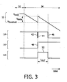
- Fig. 3 is a schematic illustration, not to scale, of waveforms employed in or resulting from operation of the current measurement circuit 1 in this embodiment.
- the waveforms shown in Fig. 3 (and also described earlier with respect to Fig. 1 ) against time are as follows: the comparator input voltage 12; the comparator output voltage 14; the feedback signal 16; and the output signal 18.
- Also indicated in Fig. 3 are a reset time stage 32 and an input current integrating time stage 34.
- Various voltage levels are indicated on the waveform of the comparator input voltage 12, namely a reset voltage V reset , voltage difference V delta , and a switching threshold voltage V threshold .
- Indicated on the waveform of the comparator output voltage 14 are a first switching 42 of the comparator output, a second switching 44 of the comparator output, and a third switching 46 of the comparator output.
- Indicated on the waveform of the feedback signal is the switching on of the feedback signal, indicated by reference numeral 48.
- Indicated on the waveform of the output signal 18 is an output pulse 50 of duration T OUT .
- the comparator input voltage 12 is reset to the reset voltage V reset .
- the current to be measured is negative, hence the reset voltage V reset is more positive than the switching threshold voltage V threshold of the comparator.
- the input current to be measured 10 is integrated by the capacitor circuit 2, and consequently the comparator input voltage 12 falls.
- the comparator input voltage 12 reaches the threshold voltage level V threshold , the comparator output voltage 14 switches for a first time, as indicated by the first switching 42 of the comparator output voltage in Fig. 3 .
- This change is applied to the logic circuit 6 which in response thereto, at step s8, switches, as indicated by reference numeral 48 in Fig. 3 , the feedback signal 16 applied to the capacitor circuit 2 from a low level to a high level (for this example in which the current to be measured 10 is a negative current).
- the change in the level of the feedback signal 16 causes the comparator input voltage 12 to rise by a known amount, namely the voltage difference V delta indicated in Fig. 3 .
- This takes the comparator input voltage 12 above the threshold voltage level V threshold once again, and at step s10 the comparator output voltage 14 switches for a second time, as indicated by the second switching 44 of the comparator output voltage 14 in Fig. 3 .
- step s12 the comparator input voltage 12 continues to fall as the input current to be measured 10 continues to be integrated.
- step s14 the comparator output voltage 14 switches for a third time, as indicated by the third switching 46 of the comparator output voltage 14 in Fig. 3 .
- step s16 generation of the output pulse 50 by the logic circuit 6 from the comparator output voltage 14 is completed.
- the output pulse 50 is generated from the timing of the switching of the comparator by taking the time between the second switching 44 and the third switching 46 of the comparator output voltage 14, to give an output pulse width (i.e. duration) T OUT as shown in Fig. 3 .
- This output pulse 50 is of a width (i.e. a duration) T OUT that is determined by the time taken for the input current to be measured 10 to change the comparator input voltage 12 by the amount of the voltage difference V delta , and this is proportional to the input current to be measured 10.
- the counter circuit 8 converts the output pulse 50, more particularly the output pulse width or duration T OUT , into a corresponding digital current value representative or indicative of the current level of the input current to be measured 10 and outputs this as digital output data 20.
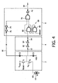
- Fig. 4 is a circuit diagram showing details of the capacitor circuit 2, the comparator circuit 4 and the logic circuit 6. Also shown in Fig. 4 is a current source 60 providing the current to be measured 10. In this embodiment the current source 60 is photo diode 60.
- the capacitor circuit 2 comprises two capacitors, hereinafter referred to as C1 and C2; and two transistors, hereinafter referred to as T1 and T2.
- Capacitor C1 is connected between the input of the comparator circuit 4 and ground.
- Capacitor C2 is connected between the input of the comparator circuit 4 and the input of the capacitor circuit 2 which is coupled to an output of the logic circuit 6 and which receives therefrom the feedback signal 16.
- the relative value of capacitors C1 and C2 determines the magnitude of the previously described voltage difference V delta .
- Transistor T1 is provided to allow the comparator input voltage 12 to be set to the previously described reset voltage level V reset (at previously described step s2) and this includes a signal "reset" at the gate of the transistor T1.
- the current to be measured 10 is applied to the capacitance at the input node of the comparator circuit 4 via the transistor T2.
- Transistor T2 isolates the input node of the comparator circuit 4 from the input of the current to be measured 10. Transistor T2 defines the voltage at the measurement input a prevents this voltage from changing significantly as the comparator input voltage 12 changes. Transistor T2 can be thought of as operating in a similar manner to a so-called cascode device, isolating the change in voltage at the input of the comparator 4 from the current input node of the circuit. However, transistor T2 is not essential, and hence in other embodiments the capacitor circuit 2 is provided without transistor T2.
- the voltage at the current input of the capacitor circuit is equal to the gate voltage V B of transistor T2 minus the gate source voltage of T2. This voltage will have a relatively small dependence on the input current value and the voltage at the input of the comparator circuit 4.
- the comparator circuit 4 is a relatively simple circuit consisting of two CMOS inverters 62 and 64 connected in series.
- the reference voltage of this circuit is the switching threshold voltage of the first inverter 62. This is approximately half way between the two power supply levels of the inverters, VDD and VSS, but depends on the transistor characteristics and is therefore not well defined.
- the logic circuit 6 of this embodiment comprises three NAND gates 66, 68 and 70, and three CMOS inverters 72, 74 and 76.
- the two NAND gates 66 and 68 together form an SR flip flop 69.
- the third NAND gate 70 is used in the generation of the previously described output pulse of 50 of the output signal 18.
- the state of the flip flop 69 is reset by a signal "nReset” at NAND gate 66 (as shown in Fig. 4 ) going low.
- the signal “nReset” is the inverse of the signal “Reset”. This reset of the signal “nReset” at NAND gate 66 occurs at the same time as the comparator input voltage 12 is set to the reset level V reset , which causes the comparator output voltage 14 to go to a high voltage level.
- the feedback signal 16 is set to a low voltage level.
- the comparator input voltage 12 starts to fall as the current to be measured 10 discharges capacitors C1 and C2.
- the comparator output voltage 14 changes from a high level to a low level. This sets the flip flop 69 causing the feedback signal 16 to go high.
- the feedback signal 16 (which is being fed back to the capacitor C2) goes from low to high the comparator input voltage 12 increases by an amount (VDD-VSS)(C2/(C2+C1)) which causes the comparator output voltage 14 to switch for a second time and to return to a high level.
- the state of the flip flop 69 is not affected by this second change in the comparator output voltage 14 and therefore the feedback signal 16 remains at a high level.
- the output signal 18 is low.
- the output signal 18 goes high when both the feedback signal 16 and the comparator output voltage 14 are high, which occurs when the comparator circuit 14 switches for the second time and it's output goes from low to high. This represents the start of output pulse 50.
- the output signal 18 goes low again (i.e. the output pulse 50 is terminated) when the comparator output voltage 14 switches for the third time.
- the width T OUT of the output pulse 50 therefore represents the time taken for the current being measured 10 to discharge the parallel combination of capacitors C1 and C2 through a voltage (VDD-VSS)(C2/(C2+C1)).
- Inverter 72 is positioned in series at the output of the NAND gate 70.
- the inverter 72 serves to buffer the output signal 18.
- Inverters 74 and 76 are in series with each other at the feedback signal 16 output of the logic circuit 6.
- the inverters 74 and 76 serve to buffer the feedback signal 16 coming from the flip flop 69 to avoid or reduce degradation of the feedback signal 16 that might otherwise arise due to it being delivered to a capacitor, namely capacitor C2, in particular since the feedback signal 16 is also used internally in the logic circuit to feed into the NAND gate 70 as part of generating the output signal 18.
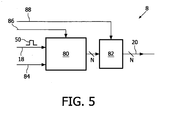
- Fig. 5 is a circuit diagram showing further details of the counter circuit 8.
- the counter circuit 8 comprises a counter 80 and a latch 82.
- the counter 80 is reset at the start of the measurement by a reset signal 86.
- the output signal 18 from the logic circuit 6 is applied to the counter 80.
- a reference clock signal 84 is also applied to the counter 80.
- the output pulse 50 contained in the output signal 18 is used to enable the counter 80.
- the period of the reference clock signal 84 determines the minimum change in the pulse width T OUT that can be resolved.
- the counter 80 is incremented during the output pulse 50 so that at the end of the measurement the state of the counter 80 represents the number of reference clock periods within the period of the pulse width T OUT .
- the state of the counter (indicated as N in Fig. 5 ) is then transferred into the latch 82 where it can be stored until required. Thereafter, under control of a latch signal 88, the state of the counter (indicated as N in Fig. 5 ) is output from the latch 82 as the previously described digital output data 20.
- hysteresis is provided between the comparator circuit 4 and the flip flop 69. This can be done to avoid that the circuit may go into oscillation at the point where the comparator circuit switches. Finite resistance of the power supply lines to the circuit may cause the power supply voltages to drop as the output signal is switched. This change in voltage may be coupled back to the input of the comparator circuit causing it to oscillate.
- the hysteresis makes the circuit more tolerant of noise on the power supply lines.
- the transistor T2 can be omitted from the capacitor circuit 2.
- the inverters 72, 74 and 76 may be omitted from the logic circuit 6.
- the sensitivity of the current measurement circuit 1 can be modified by changing the amplitude of the feedback signal 16 or the value of the capacitor C2. This is equivalent to changing the value of (VDD-VSS) or C2 in the above equation relating the current value I to the output pulse width T OUT . It may be useful to do this if a wide range of current values are desired to be measured as it avoids the tendency for the pulse width T OUT to become too short or too long.
- Fig. 6 is a circuit diagram showing details of the capacitor circuit 2, the comparator circuit 4 and the logic circuit 6 of a current measurement circuit of a further embodiment.
- the embodiment shown in Fig. 6 comprises the same elements as are present in the embodiment described earlier with reference to Fig. 4 , except where described below, and corresponding elements are labeled with the same reference numerals.
- the arrangement in Fig. 6 is the same as that of Fig. 4 , except that:
- the voltage is reset at the input of the comparator circuit 4 to a value which is close to the threshold voltage V threshold of the comparator circuit 4 as this reduces the delay before the first time that the comparator switches.
- This is achieved by connecting transistor T1 between the input and the output of the first CMOS inverter 62 in the comparator circuit 4.
- the gate of transistor T1 is driven with the signal Reset as in the Fig. 4 embodiment.
- the input and output of the first CMOS inverter 62 are connected together and the comparator input voltage becomes equal to the threshold voltage of the inverter.
- the comparator input voltage is made to go slightly above the threshold voltage. This is achieved by the capacitor C3 connected between the input of the comparator and the signal nReset. From this point onward the behavior of the circuit of Fig. 6 is the same as that of the circuit described above with reference to Fig. 4 .
- capacitor circuits can be employed instead of the above described one, to provide a function of charge integrating of the current to be measured, and in opposition thereto, charge integrating a feedback signal, the feedback signal and the current to be measured charging/integrating in an opposing or competitive sense so that the combined effect provides a measure of the strength of the current to be measured.
- capacitor C1 and hence VSS
- capacitor circuit may be omitted, with the capacitor circuit merely comprising the single capacitor C2.
- a suitable integrating circuit carrying out integrating without actual use of capacitors may be employed instead of a capacitor-based circuit as such.
- comparator circuits may be employed instead of the particular comparator circuit described above.
- Such other comparator circuits should preferably have a comparator threshold that need not be specified in an absolute sense, rather repetition in terms of the feedback cycle being more desirable.
- logic circuits may be employed instead of the particular logic circuit described above.
- the information provided by the various switching stages of the waveforms, in particular that of the comparator output voltage may be employed to give an indication or representation of the current level in ways other than the one described above in which the time between the second and third switchings or transitions of the comparator output voltage is used to initiate and terminate a pulse width.
- other timings may be used to define a pulse.
- a pulse width is used as in the above described embodiment, this need not be converted into a digital value in the manner described above.
- Other circuits or ways of converting the pulse width into a digital signal may be employed. Indeed, the pulse width or other parameter/output may be used, e.g. as an input in an automatic process, without the need to ever convert it to a digital indication as such.
- the present invention can be applied to current measurements where a simple circuit which is tolerant of variations in transistor characteristics is required or desirable. Sensor applications using large area electronics technology are one such area.
- One example is integration of light sensors onto the substrate of an active matrix display. A thin film transistor or thin film diode detects the light and passes a current which depends on the intensity of the light.
- the magnitude of this current signal can be very small making it susceptible to electrical noise from the signals applied to the display or circuits within the display module.
- the above described current measurement circuit and method can be used to convert the current from the transistor or the diode into a digital signal which is relatively insensitive to noise.
Landscapes
- Physics & Mathematics (AREA)
- General Physics & Mathematics (AREA)
- Measurement Of Current Or Voltage (AREA)
- Manipulation Of Pulses (AREA)
- Analogue/Digital Conversion (AREA)
- Support Devices For Sliding Doors (AREA)
Abstract
Claims (7)
- Dispositif (1) de mesure d'un courant, comprenant:un circuit d'intégration de charge (2);un circuit comparateur (4), dans lequel le circuit comparateur (4) comporte un inverseur (62); etun circuit logique (6) dans lequel:le circuit d'intégration de charge (2) est disposé de manière à intégrer la charge d'un courant devant être mesuré et d'appliquer un changement de potentiel en résultant à l'entrée du circuit comparateur (4);le circuit comparateur est disposé de manière à comparer le potentiel d'entrée (12) à un niveau de tension de seuil qui est le potentiel de seuil de la commutation de l'inverseur (62) en d'en générer une sortie (14) correspondante pour le circuit logique;le circuit logique est disposé de manière à générer un signal de retour (16) dépendant de la sortie du comparateur (14) et de fournir le signal de retour (16)) au circuit d'intégration de charge (2);le circuit d'intégration de charge (2) est en outre disposé de manière à intégrer une charge opposée du signal de retour reçu (16) qui est annulé par l'intégration de la charge du courant (10) à mesurer; etle circuit logique (6) est disposé en outre pour générer un signal de sortie (18) basé sur la sortie du circuit comparateur (4) et dépendant du niveau de courant (19) à mesurer , dans lequel le signal de sortie (18) généré par le circuit logique (6) comporte un pulse de sortie (50) ayant une largeur dépendant du niveau de courant à mesurer, dans lequel le pulse de sortie (50) est généré à partir de la commutation du comparateur, en considérant le temps entre une première commutation (44) et une seconde commutation (46) du potentiel de sortie du comparateur.
- Dispositif selon la revendication 1, dans lequel le dispositif comporte en outre un circuit convertisseur (8) disposé de manière à convertir le signal de sortie en une donnée numérique de sortie.
- Dispositif selon l'une quelconque des revendications 1 et 2, dans lequel le circuit d'intégration de charge comporte un transistor disposé de manière à isoler l'entrée du circuit comparateur (4) de l'entrée du courant à mesurer du circuit d'intégration de charge.
- Un dispositif de matrice active comprenant un ou plusieurs dispositifs selon l'une quelconque des revendications 1 à 3, dans lesquels le ou les dispositifs comportent des composants en film mince formés sur un substrat du dispositif de matrice active.
- Une méthode de mesure d'un courant, comprenant:un circuit d'intégration de charge (2) intégrant la charge d'un courant à mesurer (10) et appliquant un changement de potentiel en résultant à l'entrée d'un circuit comparateur (4);le circuit comparateur (4) comprenant un inverseur et comparant la tension d'entrée (12) avec un niveau de tension seuil et générant en correspondance une sortie (14) pour un circuit logique (6), le niveau de tension de seuil étant le potentiel de seuil de commutation de l'inverseur;le circuit logique (6) générant un signal de retour (16) dépendant de la sortie du comparateur (14) et fournissant le signal de retour (16) au circuit d'intégration de charge (2);le circuit d'intégration de charge (2) intégrant une charge opposée à partir du signal de retour reçu (16) )qui s'annule par l'intégration de charge du courant à mesurer; etle circuit logique (6) générant un signal de sortie (18) basé sur la sortie (14) du circuit comparateur (4) et dépendant du niveau de courant (10) à mesurer, dans lequel le signal de sortie généré par le circuit logique (6) comprend un pulse ayant une largeur dépendant du niveau du courant à mesurer, dans lequel le pulse de sortie (50) est généré à partir de la commutation du comparateur, en considérant le temps entre une première commutation (44) et une seconde commutation (46) du potentiel de sortie du comparateur.
- Une méthode selon la revendication 5, comprenant en outre un circuit convertisseur (8) convertissant le signal de sortie en une donnée de sortie numérique.
- Une méthode selon l'une quelconque des revendications 5 à 6, dans laquelle le circuit d'intégration de charge (2) comprend un transistor disposé pour isoler l'entrée du circuit comparateur de l'entrée du courant à mesurer du circuit d'intégration de charge.
Priority Applications (1)
| Application Number | Priority Date | Filing Date | Title |
|---|---|---|---|
| EP20060821423 EP1963870B1 (fr) | 2005-12-15 | 2006-11-14 | Circuit et procédé destinés à la mesure d'un courant |
Applications Claiming Priority (3)
| Application Number | Priority Date | Filing Date | Title |
|---|---|---|---|
| EP05112229 | 2005-12-15 | ||
| EP20060821423 EP1963870B1 (fr) | 2005-12-15 | 2006-11-14 | Circuit et procédé destinés à la mesure d'un courant |
| PCT/IB2006/054233 WO2007069102A2 (fr) | 2005-12-15 | 2006-11-14 | Circuit et procede destines a la mesure d'un courant |
Publications (2)
| Publication Number | Publication Date |
|---|---|
| EP1963870A2 EP1963870A2 (fr) | 2008-09-03 |
| EP1963870B1 true EP1963870B1 (fr) | 2012-07-04 |
Family
ID=38051035
Family Applications (1)
| Application Number | Title | Priority Date | Filing Date |
|---|---|---|---|
| EP20060821423 Not-in-force EP1963870B1 (fr) | 2005-12-15 | 2006-11-14 | Circuit et procédé destinés à la mesure d'un courant |
Country Status (5)
| Country | Link |
|---|---|
| US (2) | US7952343B2 (fr) |
| EP (1) | EP1963870B1 (fr) |
| JP (1) | JP5124476B2 (fr) |
| CN (1) | CN101331402B (fr) |
| WO (1) | WO2007069102A2 (fr) |
Families Citing this family (11)
| Publication number | Priority date | Publication date | Assignee | Title |
|---|---|---|---|---|
| WO2009060361A2 (fr) * | 2007-11-05 | 2009-05-14 | Koninklijke Philips Electronics N.V. | Intégrateur de courant à large portée dynamique |
| US8405407B2 (en) * | 2009-06-05 | 2013-03-26 | Chimei Innolux Corporation | Current measurement circuit and measuring method thereof including a binary weighted capacitor array |
| CA2807143C (fr) | 2010-08-04 | 2020-04-28 | Silgan Plastics Llc | Procede et appareil de moulage par soufflage pour la formation d'un recipient en plastique compressible |
| KR20140017631A (ko) * | 2011-03-29 | 2014-02-11 | 콘티넨탈 테베스 아게 운트 코. 오하게 | 전기 차량들에 있어서 공급 전압을 측정하는 디바이스 |
| TWI444628B (zh) * | 2012-03-23 | 2014-07-11 | Univ Nat Chiao Tung | 數位讀出模組、數位感測裝置 |
| CN203879127U (zh) * | 2014-05-19 | 2014-10-15 | 南京东屋电气有限公司 | 用于锁具的安全锁死机构 |
| CN104793045B (zh) * | 2015-04-23 | 2016-10-26 | 中国科学院近代物理研究所 | 一种宽量程电流频率转换器 |
| CN106707009B (zh) * | 2016-12-30 | 2020-11-13 | 南京理工大学 | 一种宽量程高精度电流统计电路 |
| US11268990B2 (en) * | 2018-12-20 | 2022-03-08 | Qorvo Us, Inc. | Current measurement circuit for optimization of power consumption in electronic devices |
| CN119559877A (zh) * | 2020-11-16 | 2025-03-04 | 群创光电股份有限公司 | 电子装置 |
| CN114089024B (zh) | 2022-01-20 | 2022-04-26 | 成都齐碳科技有限公司 | 电流测量电路、测量方法及纳米孔测序装置 |
Family Cites Families (33)
| Publication number | Priority date | Publication date | Assignee | Title |
|---|---|---|---|---|
| US321645A (en) * | 1885-07-07 | Door-check | ||
| US914065A (en) * | 1909-03-02 | Stewart J Newhart | Sash-lock. | |
| US1833236A (en) * | 1931-05-15 | 1931-11-24 | Hardsocg Wonder Drill Co | Tool retainer |
| US3768847A (en) * | 1971-07-29 | 1973-10-30 | E Buck | Security lock means |
| JPS49106268A (fr) * | 1973-02-08 | 1974-10-08 | ||
| US3976942A (en) * | 1974-12-13 | 1976-08-24 | Esterline Corporation | Watt/watt hour transducer having current signals and a modulator therefor |
| CA1079858A (fr) * | 1975-05-19 | 1980-06-17 | Adrian K. Dorsman | Convertisseur analogique-numerique |
| US4179143A (en) * | 1978-01-31 | 1979-12-18 | Shy Min C | Fixed latch lock |
| JPS5880927A (ja) * | 1981-11-09 | 1983-05-16 | Advantest Corp | 多重スロ−プ積分形ad変換器 |
| JPS59116055A (ja) | 1982-12-23 | 1984-07-04 | Omron Tateisi Electronics Co | 電圧・周波数変換回路 |
| US4565078A (en) * | 1983-03-04 | 1986-01-21 | Solomon Martin D | Lock assembly |
| US4601502A (en) * | 1985-05-06 | 1986-07-22 | Dyke James R Van | Door stop assembly |
| JPS62222175A (ja) * | 1985-12-05 | 1987-09-30 | Canon Inc | 微小信号判別装置 |
| US4688406A (en) * | 1986-04-01 | 1987-08-25 | Blumcraft Of Pittsburgh | Deadbolt lock mechanism |
| US5083091A (en) * | 1986-04-23 | 1992-01-21 | Rosemount, Inc. | Charged balanced feedback measurement circuit |
| DE8806052U1 (de) * | 1988-05-06 | 1988-09-29 | Dorma-Glas Gesellschaft für Glastürbeschläge und -Konstruktionen mbH, 4902 Bad Salzuflen | Bodentürschließer für Schwenk- und/oder Pendeltüren |
| JPH03277927A (ja) * | 1990-03-28 | 1991-12-09 | Iwasaki Electric Co Ltd | 光―周波数変換装置 |
| US5033920A (en) * | 1990-06-04 | 1991-07-23 | Tony Cantanese | Drill chuck lock apparatus |
| US5092637A (en) * | 1990-08-24 | 1992-03-03 | Miller Kermit G | Latch assembly for doors |
| DE69111800T2 (de) * | 1991-06-20 | 1995-12-14 | Hewlett Packard Gmbh | Photodiodenanordnung. |
| FR2720835B1 (fr) * | 1994-06-01 | 1996-07-12 | Schlumberger Ind Sa | Circuit de mesure de courant comprenant un transformateur à inductance mutuelle et un circuit intégrateur. |
| JP3311208B2 (ja) * | 1995-07-21 | 2002-08-05 | 株式会社東芝 | 電圧/周波数変換器 |
| US5604970A (en) * | 1995-12-26 | 1997-02-25 | Schlage Lock Company | Bolt and bar attachment method for auto assembly |
| US5936433A (en) * | 1998-01-23 | 1999-08-10 | National Semiconductor Corporation | Comparator including a transconducting inverter biased to operate in subthreshold |
| JP4374729B2 (ja) | 2000-05-16 | 2009-12-02 | ヤマハ株式会社 | 電流測定回路、使用電流量測定回路、および充放電電流測定回路 |
| JP3982342B2 (ja) * | 2002-03-28 | 2007-09-26 | ヤマハ株式会社 | D級増幅器における三角波生成回路および該三角波生成回路を用いたd級増幅器 |
| JP2004333208A (ja) | 2003-03-11 | 2004-11-25 | Fuji Electric Systems Co Ltd | 超微小電流/周波数変換装置 |
| JP4156412B2 (ja) * | 2003-03-13 | 2008-09-24 | 三菱電機株式会社 | 電流センサ |
| US6750796B1 (en) * | 2003-03-27 | 2004-06-15 | National Semiconductor Corporation | Low noise correlated double sampling modulation system |
| US6903558B1 (en) * | 2003-04-25 | 2005-06-07 | National Semiconductor Corporation | Digitizing ohmmeter system |
| GB2405701A (en) * | 2003-09-03 | 2005-03-09 | Seiko Epson Corp | Differential current sensing circuit |
| DE60330604D1 (de) * | 2003-09-12 | 2010-01-28 | Jouko Urpolahti | Verriegelungsbolzen für eine schiebetür oder dergleichen |
| US20080150302A1 (en) * | 2006-03-02 | 2008-06-26 | Chung-Liang Lin | Bolt Assembly for Lock |
-
2006
- 2006-11-14 US US12/097,433 patent/US7952343B2/en active Active
- 2006-11-14 JP JP2008545149A patent/JP5124476B2/ja not_active Expired - Fee Related
- 2006-11-14 EP EP20060821423 patent/EP1963870B1/fr not_active Not-in-force
- 2006-11-14 WO PCT/IB2006/054233 patent/WO2007069102A2/fr not_active Ceased
- 2006-11-14 CN CN2006800471643A patent/CN101331402B/zh not_active Expired - Fee Related
- 2006-11-22 US US12/097,263 patent/US20080303293A1/en not_active Abandoned
Also Published As
| Publication number | Publication date |
|---|---|
| JP5124476B2 (ja) | 2013-01-23 |
| CN101331402A (zh) | 2008-12-24 |
| US20080303293A1 (en) | 2008-12-11 |
| WO2007069102A3 (fr) | 2007-09-13 |
| US20080303507A1 (en) | 2008-12-11 |
| JP2009519463A (ja) | 2009-05-14 |
| EP1963870A2 (fr) | 2008-09-03 |
| CN101331402B (zh) | 2011-06-08 |
| US7952343B2 (en) | 2011-05-31 |
| WO2007069102A2 (fr) | 2007-06-21 |
Similar Documents
| Publication | Publication Date | Title |
|---|---|---|
| CN111928878B (zh) | 开关电阻器传感器电桥、对应的系统和方法 | |
| KR101390274B1 (ko) | 집적된 시간 및/또는 캐패시턴스 측정 시스템, 방법 및 장치 | |
| US6373264B1 (en) | Impedance detection apparatus and method of physical variable | |
| US7341374B2 (en) | Temperature measurement circuit calibrated through shifting a conversion reference level | |
| EP1963870B1 (fr) | Circuit et procédé destinés à la mesure d'un courant | |
| US10756745B2 (en) | Electrical circuit for biasing or measuring current from a sensor | |
| CN110163015B (zh) | 乘法器电路、对应的设备和方法 | |
| US4034364A (en) | Analog-digital converter | |
| EP3296709B1 (fr) | Convertisseur numérique de température | |
| KR910004656B1 (ko) | 아날로그 신호적분 및 디지탈 신호변환회로 | |
| US6756699B2 (en) | Device and method for calibrating the pulse duration of a signal source | |
| US6462598B1 (en) | Delay time control circuit | |
| JPH1038930A (ja) | ピーク電圧検出回路 | |
| EP3806331B1 (fr) | Oscillateur rc | |
| JP2003143011A (ja) | アナログ−ディジタル変換回路 | |
| JP4422284B2 (ja) | A/d変換器及び半導体圧力センサ装置 | |
| JP2674282B2 (ja) | 電子式電力量計 | |
| JPH11136129A (ja) | Pwm変換回路およびそれを用いたセンサ装置 | |
| JP3114816B2 (ja) | デジタル出力を有する容量形センサ | |
| JP3829064B2 (ja) | 静電容量型センサ | |
| JPH0334028B2 (fr) | ||
| JPH0722950A (ja) | Ad変換回路 | |
| WO1998019395A1 (fr) | Circuit de commande de temporisation | |
| JPS63236975A (ja) | デユ−テイ比測定装置 | |
| JPH03172774A (ja) | 波形測定装置 |
Legal Events
| Date | Code | Title | Description |
|---|---|---|---|
| PUAI | Public reference made under article 153(3) epc to a published international application that has entered the european phase |
Free format text: ORIGINAL CODE: 0009012 |
|
| 17P | Request for examination filed |
Effective date: 20080715 |
|
| AK | Designated contracting states |
Kind code of ref document: A2 Designated state(s): AT BE BG CH CY CZ DE DK EE ES FI FR GB GR HU IE IS IT LI LT LU LV MC NL PL PT RO SE SI SK TR |
|
| 17Q | First examination report despatched |
Effective date: 20100913 |
|
| RTI1 | Title (correction) |
Free format text: CURRENT MEASUREMENT CIRCUIT AND METHOD |
|
| GRAP | Despatch of communication of intention to grant a patent |
Free format text: ORIGINAL CODE: EPIDOSNIGR1 |
|
| DAX | Request for extension of the european patent (deleted) | ||
| GRAS | Grant fee paid |
Free format text: ORIGINAL CODE: EPIDOSNIGR3 |
|
| GRAA | (expected) grant |
Free format text: ORIGINAL CODE: 0009210 |
|
| RAP1 | Party data changed (applicant data changed or rights of an application transferred) |
Owner name: CHIMEI INNOLUX CORPORATION |
|
| AK | Designated contracting states |
Kind code of ref document: B1 Designated state(s): AT BE BG CH CY CZ DE DK EE ES FI FR GB GR HU IE IS IT LI LT LU LV MC NL PL PT RO SE SI SK TR |
|
| REG | Reference to a national code |
Ref country code: GB Ref legal event code: FG4D |
|
| REG | Reference to a national code |
Ref country code: CH Ref legal event code: EP |
|
| REG | Reference to a national code |
Ref country code: AT Ref legal event code: REF Ref document number: 565356 Country of ref document: AT Kind code of ref document: T Effective date: 20120715 |
|
| REG | Reference to a national code |
Ref country code: IE Ref legal event code: FG4D |
|
| REG | Reference to a national code |
Ref country code: DE Ref legal event code: R096 Ref document number: 602006030599 Country of ref document: DE Effective date: 20120830 |
|
| REG | Reference to a national code |
Ref country code: NL Ref legal event code: T3 |
|
| REG | Reference to a national code |
Ref country code: AT Ref legal event code: MK05 Ref document number: 565356 Country of ref document: AT Kind code of ref document: T Effective date: 20120704 |
|
| PG25 | Lapsed in a contracting state [announced via postgrant information from national office to epo] |
Ref country code: SI Free format text: LAPSE BECAUSE OF FAILURE TO SUBMIT A TRANSLATION OF THE DESCRIPTION OR TO PAY THE FEE WITHIN THE PRESCRIBED TIME-LIMIT Effective date: 20120704 |
|
| REG | Reference to a national code |
Ref country code: LT Ref legal event code: MG4D Effective date: 20120704 |
|
| PG25 | Lapsed in a contracting state [announced via postgrant information from national office to epo] |
Ref country code: AT Free format text: LAPSE BECAUSE OF FAILURE TO SUBMIT A TRANSLATION OF THE DESCRIPTION OR TO PAY THE FEE WITHIN THE PRESCRIBED TIME-LIMIT Effective date: 20120704 Ref country code: FI Free format text: LAPSE BECAUSE OF FAILURE TO SUBMIT A TRANSLATION OF THE DESCRIPTION OR TO PAY THE FEE WITHIN THE PRESCRIBED TIME-LIMIT Effective date: 20120704 Ref country code: CY Free format text: LAPSE BECAUSE OF FAILURE TO SUBMIT A TRANSLATION OF THE DESCRIPTION OR TO PAY THE FEE WITHIN THE PRESCRIBED TIME-LIMIT Effective date: 20120704 Ref country code: LT Free format text: LAPSE BECAUSE OF FAILURE TO SUBMIT A TRANSLATION OF THE DESCRIPTION OR TO PAY THE FEE WITHIN THE PRESCRIBED TIME-LIMIT Effective date: 20120704 Ref country code: BE Free format text: LAPSE BECAUSE OF FAILURE TO SUBMIT A TRANSLATION OF THE DESCRIPTION OR TO PAY THE FEE WITHIN THE PRESCRIBED TIME-LIMIT Effective date: 20120704 Ref country code: IS Free format text: LAPSE BECAUSE OF FAILURE TO SUBMIT A TRANSLATION OF THE DESCRIPTION OR TO PAY THE FEE WITHIN THE PRESCRIBED TIME-LIMIT Effective date: 20121104 |
|
| PG25 | Lapsed in a contracting state [announced via postgrant information from national office to epo] |
Ref country code: LV Free format text: LAPSE BECAUSE OF FAILURE TO SUBMIT A TRANSLATION OF THE DESCRIPTION OR TO PAY THE FEE WITHIN THE PRESCRIBED TIME-LIMIT Effective date: 20120704 Ref country code: PT Free format text: LAPSE BECAUSE OF FAILURE TO SUBMIT A TRANSLATION OF THE DESCRIPTION OR TO PAY THE FEE WITHIN THE PRESCRIBED TIME-LIMIT Effective date: 20121105 Ref country code: GR Free format text: LAPSE BECAUSE OF FAILURE TO SUBMIT A TRANSLATION OF THE DESCRIPTION OR TO PAY THE FEE WITHIN THE PRESCRIBED TIME-LIMIT Effective date: 20121005 Ref country code: PL Free format text: LAPSE BECAUSE OF FAILURE TO SUBMIT A TRANSLATION OF THE DESCRIPTION OR TO PAY THE FEE WITHIN THE PRESCRIBED TIME-LIMIT Effective date: 20120704 Ref country code: SE Free format text: LAPSE BECAUSE OF FAILURE TO SUBMIT A TRANSLATION OF THE DESCRIPTION OR TO PAY THE FEE WITHIN THE PRESCRIBED TIME-LIMIT Effective date: 20120704 |
|
| PGFP | Annual fee paid to national office [announced via postgrant information from national office to epo] |
Ref country code: IT Payment date: 20121122 Year of fee payment: 7 |
|
| PG25 | Lapsed in a contracting state [announced via postgrant information from national office to epo] |
Ref country code: ES Free format text: LAPSE BECAUSE OF FAILURE TO SUBMIT A TRANSLATION OF THE DESCRIPTION OR TO PAY THE FEE WITHIN THE PRESCRIBED TIME-LIMIT Effective date: 20121015 Ref country code: EE Free format text: LAPSE BECAUSE OF FAILURE TO SUBMIT A TRANSLATION OF THE DESCRIPTION OR TO PAY THE FEE WITHIN THE PRESCRIBED TIME-LIMIT Effective date: 20120704 Ref country code: CZ Free format text: LAPSE BECAUSE OF FAILURE TO SUBMIT A TRANSLATION OF THE DESCRIPTION OR TO PAY THE FEE WITHIN THE PRESCRIBED TIME-LIMIT Effective date: 20120704 Ref country code: DK Free format text: LAPSE BECAUSE OF FAILURE TO SUBMIT A TRANSLATION OF THE DESCRIPTION OR TO PAY THE FEE WITHIN THE PRESCRIBED TIME-LIMIT Effective date: 20120704 Ref country code: RO Free format text: LAPSE BECAUSE OF FAILURE TO SUBMIT A TRANSLATION OF THE DESCRIPTION OR TO PAY THE FEE WITHIN THE PRESCRIBED TIME-LIMIT Effective date: 20120704 |
|
| PLBE | No opposition filed within time limit |
Free format text: ORIGINAL CODE: 0009261 |
|
| STAA | Information on the status of an ep patent application or granted ep patent |
Free format text: STATUS: NO OPPOSITION FILED WITHIN TIME LIMIT |
|
| PG25 | Lapsed in a contracting state [announced via postgrant information from national office to epo] |
Ref country code: SK Free format text: LAPSE BECAUSE OF FAILURE TO SUBMIT A TRANSLATION OF THE DESCRIPTION OR TO PAY THE FEE WITHIN THE PRESCRIBED TIME-LIMIT Effective date: 20120704 |
|
| 26N | No opposition filed |
Effective date: 20130405 |
|
| REG | Reference to a national code |
Ref country code: CH Ref legal event code: PL |
|
| PG25 | Lapsed in a contracting state [announced via postgrant information from national office to epo] |
Ref country code: LI Free format text: LAPSE BECAUSE OF NON-PAYMENT OF DUE FEES Effective date: 20121130 Ref country code: BG Free format text: LAPSE BECAUSE OF FAILURE TO SUBMIT A TRANSLATION OF THE DESCRIPTION OR TO PAY THE FEE WITHIN THE PRESCRIBED TIME-LIMIT Effective date: 20121004 Ref country code: CH Free format text: LAPSE BECAUSE OF NON-PAYMENT OF DUE FEES Effective date: 20121130 |
|
| REG | Reference to a national code |
Ref country code: DE Ref legal event code: R097 Ref document number: 602006030599 Country of ref document: DE Effective date: 20130405 |
|
| REG | Reference to a national code |
Ref country code: IE Ref legal event code: MM4A |
|
| PG25 | Lapsed in a contracting state [announced via postgrant information from national office to epo] |
Ref country code: IE Free format text: LAPSE BECAUSE OF NON-PAYMENT OF DUE FEES Effective date: 20121114 |
|
| PG25 | Lapsed in a contracting state [announced via postgrant information from national office to epo] |
Ref country code: TR Free format text: LAPSE BECAUSE OF FAILURE TO SUBMIT A TRANSLATION OF THE DESCRIPTION OR TO PAY THE FEE WITHIN THE PRESCRIBED TIME-LIMIT Effective date: 20120704 Ref country code: MC Free format text: LAPSE BECAUSE OF NON-PAYMENT OF DUE FEES Effective date: 20121130 |
|
| PG25 | Lapsed in a contracting state [announced via postgrant information from national office to epo] |
Ref country code: LU Free format text: LAPSE BECAUSE OF NON-PAYMENT OF DUE FEES Effective date: 20121114 |
|
| PG25 | Lapsed in a contracting state [announced via postgrant information from national office to epo] |
Ref country code: HU Free format text: LAPSE BECAUSE OF FAILURE TO SUBMIT A TRANSLATION OF THE DESCRIPTION OR TO PAY THE FEE WITHIN THE PRESCRIBED TIME-LIMIT Effective date: 20061114 |
|
| PG25 | Lapsed in a contracting state [announced via postgrant information from national office to epo] |
Ref country code: IT Free format text: LAPSE BECAUSE OF NON-PAYMENT OF DUE FEES Effective date: 20131114 |
|
| REG | Reference to a national code |
Ref country code: FR Ref legal event code: PLFP Year of fee payment: 10 |
|
| REG | Reference to a national code |
Ref country code: FR Ref legal event code: PLFP Year of fee payment: 11 |
|
| REG | Reference to a national code |
Ref country code: FR Ref legal event code: PLFP Year of fee payment: 12 |
|
| REG | Reference to a national code |
Ref country code: FR Ref legal event code: PLFP Year of fee payment: 13 |
|
| PGFP | Annual fee paid to national office [announced via postgrant information from national office to epo] |
Ref country code: NL Payment date: 20191114 Year of fee payment: 14 Ref country code: DE Payment date: 20191029 Year of fee payment: 14 |
|
| PGFP | Annual fee paid to national office [announced via postgrant information from national office to epo] |
Ref country code: FR Payment date: 20191014 Year of fee payment: 14 |
|
| PGFP | Annual fee paid to national office [announced via postgrant information from national office to epo] |
Ref country code: GB Payment date: 20191115 Year of fee payment: 14 |
|
| REG | Reference to a national code |
Ref country code: DE Ref legal event code: R119 Ref document number: 602006030599 Country of ref document: DE |
|
| REG | Reference to a national code |
Ref country code: NL Ref legal event code: MM Effective date: 20201201 |
|
| GBPC | Gb: european patent ceased through non-payment of renewal fee |
Effective date: 20201114 |
|
| PG25 | Lapsed in a contracting state [announced via postgrant information from national office to epo] |
Ref country code: NL Free format text: LAPSE BECAUSE OF NON-PAYMENT OF DUE FEES Effective date: 20201201 |
|
| PG25 | Lapsed in a contracting state [announced via postgrant information from national office to epo] |
Ref country code: FR Free format text: LAPSE BECAUSE OF NON-PAYMENT OF DUE FEES Effective date: 20201130 |
|
| PG25 | Lapsed in a contracting state [announced via postgrant information from national office to epo] |
Ref country code: DE Free format text: LAPSE BECAUSE OF NON-PAYMENT OF DUE FEES Effective date: 20210601 Ref country code: GB Free format text: LAPSE BECAUSE OF NON-PAYMENT OF DUE FEES Effective date: 20201114 |