EP1965251A1 - Dispositif de rétro-éclairage par DEL et dispositif à LCD - Google Patents
Dispositif de rétro-éclairage par DEL et dispositif à LCD Download PDFInfo
- Publication number
- EP1965251A1 EP1965251A1 EP08101946A EP08101946A EP1965251A1 EP 1965251 A1 EP1965251 A1 EP 1965251A1 EP 08101946 A EP08101946 A EP 08101946A EP 08101946 A EP08101946 A EP 08101946A EP 1965251 A1 EP1965251 A1 EP 1965251A1
- Authority
- EP
- European Patent Office
- Prior art keywords
- led
- substrate
- anode
- cathode
- film layered
- Prior art date
- Legal status (The legal status is an assumption and is not a legal conclusion. Google has not performed a legal analysis and makes no representation as to the accuracy of the status listed.)
- Granted
Links
Images




Classifications
-
- G—PHYSICS
- G02—OPTICS
- G02F—OPTICAL DEVICES OR ARRANGEMENTS FOR THE CONTROL OF LIGHT BY MODIFICATION OF THE OPTICAL PROPERTIES OF THE MEDIA OF THE ELEMENTS INVOLVED THEREIN; NON-LINEAR OPTICS; FREQUENCY-CHANGING OF LIGHT; OPTICAL LOGIC ELEMENTS; OPTICAL ANALOGUE/DIGITAL CONVERTERS
- G02F1/00—Devices or arrangements for the control of the intensity, colour, phase, polarisation or direction of light arriving from an independent light source, e.g. switching, gating or modulating; Non-linear optics
- G02F1/01—Devices or arrangements for the control of the intensity, colour, phase, polarisation or direction of light arriving from an independent light source, e.g. switching, gating or modulating; Non-linear optics for the control of the intensity, phase, polarisation or colour
- G02F1/13—Devices or arrangements for the control of the intensity, colour, phase, polarisation or direction of light arriving from an independent light source, e.g. switching, gating or modulating; Non-linear optics for the control of the intensity, phase, polarisation or colour based on liquid crystals, e.g. single liquid crystal display cells
- G02F1/133—Constructional arrangements; Operation of liquid crystal cells; Circuit arrangements
- G02F1/1333—Constructional arrangements; Manufacturing methods
- G02F1/1335—Structural association of cells with optical devices, e.g. polarisers or reflectors
- G02F1/1336—Illuminating devices
- G02F1/133617—Illumination with ultraviolet light; Luminescent elements or materials associated to the cell
-
- G—PHYSICS
- G02—OPTICS
- G02F—OPTICAL DEVICES OR ARRANGEMENTS FOR THE CONTROL OF LIGHT BY MODIFICATION OF THE OPTICAL PROPERTIES OF THE MEDIA OF THE ELEMENTS INVOLVED THEREIN; NON-LINEAR OPTICS; FREQUENCY-CHANGING OF LIGHT; OPTICAL LOGIC ELEMENTS; OPTICAL ANALOGUE/DIGITAL CONVERTERS
- G02F1/00—Devices or arrangements for the control of the intensity, colour, phase, polarisation or direction of light arriving from an independent light source, e.g. switching, gating or modulating; Non-linear optics
- G02F1/01—Devices or arrangements for the control of the intensity, colour, phase, polarisation or direction of light arriving from an independent light source, e.g. switching, gating or modulating; Non-linear optics for the control of the intensity, phase, polarisation or colour
- G02F1/13—Devices or arrangements for the control of the intensity, colour, phase, polarisation or direction of light arriving from an independent light source, e.g. switching, gating or modulating; Non-linear optics for the control of the intensity, phase, polarisation or colour based on liquid crystals, e.g. single liquid crystal display cells
- G02F1/133—Constructional arrangements; Operation of liquid crystal cells; Circuit arrangements
- G02F1/1333—Constructional arrangements; Manufacturing methods
- G02F1/1335—Structural association of cells with optical devices, e.g. polarisers or reflectors
- G02F1/1336—Illuminating devices
- G02F1/133602—Direct backlight
- G02F1/133603—Direct backlight with LEDs
-
- H—ELECTRICITY
- H05—ELECTRIC TECHNIQUES NOT OTHERWISE PROVIDED FOR
- H05B—ELECTRIC HEATING; ELECTRIC LIGHT SOURCES NOT OTHERWISE PROVIDED FOR; CIRCUIT ARRANGEMENTS FOR ELECTRIC LIGHT SOURCES, IN GENERAL
- H05B45/00—Circuit arrangements for operating light-emitting diodes [LED]
- H05B45/30—Driver circuits
- H05B45/345—Current stabilisation; Maintaining constant current
Definitions
- This invention relates to an LED backlight device and an LCD device using the LED backlight device.
- a light is emitted by a light source, and is incident on an LCD panel.
- the LCD device is configured to change molecular alignments of liquid crystals (pixels) arranged on the LCD panel, so as to display an image using the light passing through the LCD panel.
- the light source used in such an LCD device is called as a backlight, since the light source is disposed on the backside of the LCD panel (i.e., the side opposite to a display surface of the LCD panel).
- the conventional light source is composed of a cold cathode ray tube or a semiconductor light emitting element.
- the light source using the semiconductor light emitting element has been broadly used, since such a light source has a long lifetime and contributes to reduction of power consumption.
- a surface-emitting light source that uses an LED (Light Emitting Diode) as the above described semiconductor light emitting element.
- a surface-emitting light source has a plate-like member called as a light guiding plate or a light diffusion plate for guiding the light emitted by the LED.
- the light emitted by the LED is incident on an end surface of the light guiding plate.
- the light guiding plate reflects and diffuses the incident light in the direction perpendicular to the surface of the light guiding plate, and emits the light from a surface thereof (see Patent Document No. 1).
- Patent Document No. 1 Japanese Laid-Open Patent Publication No. 11-232920 .
- the light diffused in the interior of the light guiding plate tends to attenuate due to the reflection and diffusion, as a distance from the incident surface (i.e., the end surface of the light guiding plate) increases. Therefore, in order to obtain a high light intensity uniformly over the entire surface, the structure of the light guiding plate needs to be complicated, and the LED backlight device needs to be thick.
- the present invention is intended to solve the above described problems, and an object of the present invention is to provide a thin LED backlight device capable of providing a high light intensity, and an LCD device using such an LED backlight.
- the present invention provides a backlight device including a substrate having an optical transparency and having a first surface and a second surface opposite to the first surface, an LED thin-film layered structure formed on the first surface of the substrate, the LED thin-film layered structure being formed of epitaxially grown inorganic material layers as a P-N junction device, an anode electrode and a cathode electrode formed on the LED thin-film layered structure, an anode driver IC and a cathode driver IC for driving the LED thin-film layered structure, a wiring structure that electrically connects the anode driver IC and the anode electrode of the LED thin-film layered structure and electrically connects the cathode driver IC and the cathode electrode of the LED thin-film layered structure, and a phosphor formed on the second surface of the substrate.
- the LED backlight device has the phosphor formed on the second surface of the substrate (having an optical transparency) opposite to the first surface on which the LED thin-film layered structure is formed, it becomes possible to obtain a thin LED backlight device providing a high light intensity.
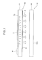
- FIG. 1 is a side sectional view showing a main part of an LCD device including an LED backlight device according to the first embodiment of the present invention.
- FIG. 2 is a perspective view showing the LED backlight device according to the first embodiment of the present invention, as seen from a first surface side.
- FIG. 3 is a perspective view showing the LED backlight device according to the first embodiment of the present invention, as seen from a second surface side.
- an LED backlight device 100 is used as a light source in a LCD device 101, and is disposed on a backside of an LCD panel 102 (i.e., the side opposite to a display surface 102a of the LCD panel 102).
- the LCD panel 102 is of a transmission type.
- the LED backlight device 100 includes a substrate 10 in the form of a flat plate.
- the LED backlight device 100 further includes an LED 11 (i.e., an LED thin-film layered structure) fixed to a first surface of the substrate 10 (i.e., an upper surface in FIG. 1 ), and a phosphor 30 fixed to a second surface of the substrate 10 (i.e., a lower surface of in FIG. 1 ).
- an anode driver IC 31 and a cathode driver IC 32 for driving the LED 11 are disposed on the first surface of the substrate 10.
- the anode driver IC 31 is connected to an end of an anode wiring 12 (formed on the first surface of the substrate 10) connected to an anode electrode 14 of the LED 11.
- the cathode driver IC 32 is connected to an end of a cathode wiring 13 (formed on the first surface of the substrate 10) connected to a cathode electrode 15 of the LED 11.
- the anode wiring 12 and the cathode wiring 13 constitute a wiring structure for electrically connecting the anode driver IC 31 to the LED 11, and for electrically connecting the cathode driver IC 32 to the LED 11.
- the substrate 10 is formed of a plate having an optical transparency composed of a quarts or glass.
- the phosphor 30 emits white light when exposed to near-ultraviolet or ultraviolet rays.
- the phosphor 30 is coated on the second surface of the substrate 10.
- the phosphor 30 can be formed by mixing a phosphor that emits red light, a phosphor that emits green light and a phosphor that emits blue light.
- the phosphor that emits red light is, for example, Y 2 O 3 : Eu or (Y, Gd) BO 3 : Eu.
- the phosphor that emits green light is, for example, LaPO 4 : Ce, Tb or Zn 2 SiO : Mn.
- the phosphor that emits blue light is, for example, (Sr, Ca, Ba, Mg) 5 (PO 4 ) 3 Cl : Eu or BaMgAl 10 O 17 : Eu.
- the phosphor that emits red light is not limited the above described material, but can be composed of any kind of material that emits light having the wavelength ranging from 620 nm to 710 nm when exposed to near-ultraviolet or ultraviolet rays having the wavelength ranging from 300 nm to 450 nm.
- the phosphor that emits green light can be composed of any kind of material that emits light having the wavelength ranging from 500 nm to 580 nm when exposed to near-ultraviolet or ultraviolet rays having the wavelength ranging from 300 nm to 450 nm.
- the phosphor that emits blue light can be composed of any kind of material that emits light having the wavelength ranging from 450 nm to 500 nm when exposed to near-ultraviolet or ultraviolet rays having the wavelength ranging from 300 nm to 450 nm.
- the first surface of the substrate 10 is composed of a surface layer 10a ( FIG. 1 ) having an optical transparency formed of an organic insulation film (such as polyimide film or the like) or an inorganic insulation film formed thereon.
- the surface layer 10a is planarized to a surface accuracy less than or equal to several tens of nanometers, and has no convex or concaves.
- the LED 11 is peeled off from another substrate (i.e., a base material) as described later, and is fixed to the substrate 10 by means of intermolecular force such as hydrogen bonding, so that the LED 11 is integrated with the substrate 10.
- the above described LED 11 is a thin-film LED that emits near-ultraviolet rays or ultraviolet rays, and is composed of a thin-film layered structure having a heterostructure or a double-heterostructure formed by epitaxially growing inorganic material such as gallium nitride, gallium indium nitride, aluminum gallium nitride, aluminum nitride or the like.
- the LED 11 is not limited to the above described material, but can be composed of any kind of material that emits near-ultraviolet rays or ultraviolet rays, more preferably, the light having the wavelength ranging from 300 to 450 nm.
- the LED 11 and the phosphor 30 are respectively formed on the first and second surfaces of the substrate 10 so that the LED 11 and the phosphor 30 face each other.
- the phosphor 30 (facing the LED 11) emits white light as shown by arrows B in FIG. 1 .
- the anode electrode 14 and the cathode electrode 15 are metal electrodes composed of gold, aluminum, or layered metal electrodes composed of gold or aluminum layered with nickel, titan or the like.
- the anode electrode 14 and the cathode electrode 15 are respectively connected to an anode and a cathode of the LED 11.
- the anode wiring 12 and the cathode wiring 13 are metal wirings composed of gold, aluminum, or layered metal wirings composed of gold or aluminum layered with nickel, titan or the like.
- the anode wiring 12 and the cathode wiring 13 are respectively connected to the anode electrode 14 and the cathode electrode 15 of the LED 11.
- An end of the anode wiring 12 is connected the anode driver IC 31, and an end of the cathode wiring 13 is connected the cathode driver IC 32, so that the anode electrode 14 and the cathode electrode 15 of the LED 11 are connected to the anode driver IC 31 and the cathode driver IC 32 via the anode wiring 12 and the cathode wiring 13.
- the anode driver IC 31 has a function to supply electric current to the LED 11 according to a lighting signal.
- a shift register circuit, a latch circuit, a constant current circuit, an amplifier circuit and the like are integrated.
- the anode wiring 12 is connected to the anode electrode 14 of the LED and is also connected to a driving element of the anode driver IC 31.
- the anode driver IC 31 is mounted on the substrate 10 in the example shown in FIG. 2 , the anode driver IC 31 is not necessarily provided on the substrate 10, but can be provided on other print circuit board (not shown) or the like.
- the cathode driver IC 32 has a function to allow the electric current to flow therein.
- switching circuits such as transistor or the like are integrated.
- the cathode wiring 13 is connected to the cathode electrode 15 of the LED 11 and is also connected to the cathode driver IC 32.
- the cathode driver IC 32 is not necessarily provided on the substrate 10, but can be provided on other print circuit board (not shown) or the like.
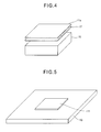
- FIG. 4 shows a process for peeling a thin-film layered structure (the LED 11) according to the first embodiment of the present invention.
- FIG. 5 shows a process for fixing the thin-film layered structure (the LED 11) to the substrate according to the first embodiment of the present invention.
- the LED 11 is made of a thin-film layered structure in the form of a rectangular flat plate, and is integrally fixed to the substrate 10 as described later. Further, the LED 11 is a thin-film layered structure that emits near-ultraviolet rays or ultraviolet rays, and has heterostructure or double-heterostructure composed of a plurality of layers such as gallium nitride or indium gallium nitride, aluminum gallium nitride, aluminum nitride or the like.
- a sacrificial layer 17 is provided between a base material 16 and the LED 11 for peeling (i.e., separating) the LED 11 from the base material 16.
- the sacrificial layer 17 is composed of material such as, for example, aluminum arsenide that can easily be etched by an etching solution described later.
- the base material 16 is composed of, for example, gallium arsenide, gallium nitride, sapphire or the like.
- a thin-film layered structure 11a of inorganic material layers (that becomes the LED 11) is epitaxially grown on the base material 16 using a vapor-phase growth method such as an MOCVD method.
- the thin-film layered structure 11a is formed to have a width and a length greater than or equal to 20 mm.
- the thin-film layered structure 11a is formed in a rectangular shape on the base material 16 using an etching solution such as a solution containing phosphoric acid, hydrogen peroxide and water (H 3 PO 4 :H 2 O 2 :H 2 O) or the like, by means of photolithographic etching technique broadly used in a semiconductor manufacturing process.
- the base material 16 on which the thin-film layered structure 11a is formed is immersed in an etching solution such as hydrogen fluoride solution, hydrochloric solution or the like. With this, the sacrificial surface 17 is etched, and the thin-film layered structure 11a (i.e., the LED 11) is peeled off from the base material 16.
- an etching solution such as hydrogen fluoride solution, hydrochloric solution or the like.
- the LED 11 (having been peeled off from the base material 16) is pressed against the planarized first surface of the substrate 10, and the substrate 10 and the LED 11 are fixed to each other by means of intermolecular force and integrated with each other.
- the surface of the substrate 10 is composed of the surface layer 10a formed of an organic insulation film such as polyimide film or an inorganic insulation film such as silicon oxide firm, and preferably is a flat surface whose surface accuracy is less than or equal to several tens of nanometers having no concaves or convexes. Since the surface of the substrate 10 is such a flat surface having no concave or convex, the bonding between the LED 11 and the substrate 10 by means of intermolecular force (such as hydrogen bonding or the like) can be facilitated. With this, as shown in FIG. 5 , the square shaped LED 11 is fixed to and integrated with the substrate 10.
- an organic insulation film such as polyimide film or an inorganic insulation film such as silicon oxide firm
- connecting portions of the anode electrode 14 and the cathode electrode 15 are formed on the LED 11 (having been fixed to the substrate 10) using, for example, a photolithographic etching method by means of an etching solution containing phosphoric acid and hydrogen peroxide and water (H 3 PO 4 :H 2 O 2 :H 2 O). Further, the anode electrode 14 and the cathode electrode 15, and the anode wiring 12 (connected to the anode electrode 14) and the cathode wiring 13 (connected to the cathode electrode 15) are formed using a deposition, a photolithographic etching method or a lift-off method.
- anode driver IC 31 and the cathode driver IC 32 are mounted to the substrate 10, and the anode wiring 12 and the cathode wiring 13 are respectively connected to the anode driver IC 31 and the cathode driver IC 32.
- an amplifier circuit of the anode driver IC 31 applies a constant current to the anode electrode 14 of the LED 11 via the anode wiring 12.
- the cathode driver IC 32 applies the current to flow therein from the cathode electrode 15 of the LED 11 via the cathode wiring 13, so that the LED 11 emits the light.
- the phosphor 30 (facing the LED 11) is excited by the near-ultraviolet rays or ultraviolet rays, and the phosphor 30 emits white light as shown by the arrows B in FIG. 1 .
- the LCD panel 102 provided in opposition to the LED backlight device 10 is illuminated by the light (emitted by the phosphor 30) from the backside of the LED panel 102.
- the LED 11, the anode wiring 12 and the cathode wiring 13 are formed on the substrate 10 having an optical transparency, and the LED 11 are connected to and the anode wirings 12 and the cathode wirings 13 using the semiconductor process, and therefore it becomes possible to accomplish a thinner LED backlight device 100.
- the LED element is known as an element having a high luminance and consuming less electric power, and has a record of performance. Using such a LED element as the light source, it becomes possible to obtain a luminance that can not be accomplished by the conventional light emitting device such as an organic EL (Electric Luminescence) element.
- organic EL Electro Luminescence
- FIG. 6 is a side sectional view showing the LED backlight device according to the second embodiment of the present invention.
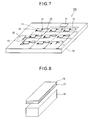
- FIG. 7 is a perspective view showing the LED backlight device according to the second embodiment of the present invention, as seen from the first surface side.
- the LED backlight device 100 has a plurality of LEDs 11.
- the LEDs 11 are arranged in rows and columns (to form an LED array) on the first surface of the substrate 10 as shown in FIG. 7 .
- the LED array on the substrate 10 includes LEDs 11 arranged at equal intervals in a square grid and in a matrix with 3 rows and 3 columns.
- the anode wiring 12 having an end connected to the anode driver IC 31 is branched into a plurality of branch lines (in this example, three branch lines).
- the respective branch lines extend along the respective columns and are connected to the anode electrodes 14 of the respective LEDs 11 of the respective columns.
- the anode electrodes 14 and the branch lines of the anode wiring 12 are connected via constant current elements 23.
- the constant current elements 23 are composed of electric resistances or the like, and are mounted to positions in the vicinities of the respective LEDs 11 on the substrate 10.
- the anode driver IC 31 has a switching circuit of a large capacity capable of supplying ON-voltage to all of the constant current elements 23 according to the lighting signals, and supplying current to all of the LEDs 11.
- the cathode wiring 13 having an end connected to the cathode driver IC 32 is branched into a plurality of branch lines (in this example, three branch lines).
- the respective branch lines extend along the respective rows and are connected to the cathode electrodes 15 of the respective LEDs 11 of the respective rows.
- the cathode driver IC 32 has a switching circuit of a large capacity capable of allowing the current from all of the LEDs 11 to flow into the switching circuit.
- the anode driver IC 31 and the cathode driver IC 32 are provided on the substrate 10.
- the anode driver IC 31 and the cathode driver IC 32 are not necessarily provided on the substrate 10, but can be provided on other print circuit board or the like.
- LED backlight device 100 of the second embodiment are the same as those of the first embodiment, and description thereof are omitted.
- FIG. 8 shows a process for peeling the thin-film layered structure (i.e., the LEDs 11) according to the second embodiment of the present invention.
- FIG. 9 shows a process for fixing the thin-film layered structure to the substrate 10 according to the second embodiment of the present invention.
- FIG. 10 shows a process for dividing the thin-film layered structure according to the second embodiment of the present invention.
- a thin-film layered structure 18 in the form of an elongated band or a strip is fixed to the substrate 10, and then divided into a plurality of LEDs 11 as described later.
- the thin-film layered structure 18 i.e., the LEDs 11
- the thin-film layered structure 18 emits near-ultraviolet rays or ultraviolet rays, and is formed of a thin-film layered structure having heterostructure or double-heterostructure composed of a plurality of layers such as gallium nitride or indium gallium nitride, aluminum gallium nitride or aluminum nitride and the like.
- the numeral 17 indicates a sacrificial layer formed between the base material 16 and the thin-film layered structure 18 as was described in the first embodiment.
- the sacrificial layer 17 is composed of material such as, for example, aluminum arsenide that can easily be etched by an etching solution described later.
- the base material 16 is composed of, for example, gallium arsenide, gallium nitride or sapphire.
- the thin-film layered structure 18 of inorganic material layers (that becomes the LEDs 11) is epitaxially grown on the base material 16 using a vapor-phase growth method such as an MOCVD method.
- the thin-film layered structure is formed into a strip shape having a width greater than or equal to 2 mm and a length greater than or equal to the length of a column of the LED array (i.e., a column including three LEDs 11).
- the thin-film layered structure 18 is formed in the strip shape on the base material 16 using the etching solution such as a solution containing phosphoric acid, hydrogen peroxide and water (H 3 PO 4 :H 2 O 2 :H 2 O), by means of the photolithographic etching technique broadly used in the semiconductor manufacturing process.
- the base material 16 on which the thin-film layered structure 18 is formed is immersed in the etching solution such as hydrogen fluoride solution or hydrochloric solution or the like. With this, the sacrificial surface 17 is etched, and the thin-film layered structure 18 is peeled off from the base material 16.
- the etching solution such as hydrogen fluoride solution or hydrochloric solution or the like.
- the thin-film layered structure 18 (having been peeled off from the base material 16) is pressed against the first surface of the substrate 10 having been planarized, and the substrate 10 and the thin-film layered structure 18 are fixed to and integrated with each other by means of intermolecular force such as hydrogen bonding.
- the first surface of the substrate 10 is formed of the surface layer 10a having an optical transparency composed of an organic insulation film (such as polyimide film or the like) or an inorganic insulation film (such as silicon oxide film or the like).
- the surface layer 10a is preferably planarized to a surface accuracy less than or equal to several tens of nanometers, and has no concaves or convexes, as was described in the first embodiment. Since the surface of the substrate 10 is such a flat surface having no concave or convex, the bonding between the thin-film layered structure 18 and the substrate 10 by means of intermolecular force (such as hydrogen bonding) can be facilitated.
- the thin-film layered structures 18 of a plurality of columns are fixed to and integrated with the first surface of the substrate 10.
- each thin-film layered structure 18 fixed to the first surface of the substrate 10 is divided into a plurality of parts to thereby form a plurality of LEDs 11 using a photolithographic etching method by means of an etching solution containing phosphoric acid and hydrogen peroxide and water (H 3 PO 4 :H 2 O 2 :H 2 O).
- each thin-film layered structure 18 is divided into three LEDs 11. With this, as shown in FIG. 10 , the LED array including the LEDs 11 arranged at equal intervals in a square grid and in a matrix of 3 rows and 3 columns on the first surface of the substrate 10 can be obtained.
- the anode electrode 14 and the cathode electrode 15 of the respective LEDs 11, and the anode wiring 12 (connected to the anode electrode 14) and the cathode wiring 13 (connected to the cathode electrode 15) are formed using a deposition, a photolithographic etching method or a lift-off method.
- the anode electrode 14 and the cathode electrode 15 are metal electrodes composed of gold, aluminum, or layered metal electrodes composed of gold or aluminum layered with nickel, titan or the like.
- the anode electrodes 14 of the respective LEDs 11 are connected to the anode driver IC 31 via the constant current elements 23 and the anode wiring 12, the cathode electrodes 15 of the respective LEDs 11 are connected to the cathode driver IC 32 via the cathode wiring 13.
- each strip-shaped thin-film layered structure 18 is divided into the square-shaped LEDs 11.
- the LED 11 can have any shape such as an elongated rectangle, a rhomboidal shape or the like.
- the amplifier circuit of the anode driver IC 31 applies ON voltage to all of the constant current elements 23 via the anode wiring 12, and apply current to all of the LEDs 11.
- the switching circuit of the cathode driver IC 32 operates to allow the current to flow therein from the LEDs 11 via the cathode wiring 13. Therefore, current flows through all of the LEDs 11, so that the LEDs 11 emit the light.
- the phosphor 30 (facing the LEDs 11) is excited by the near-ultraviolet rays or ultraviolet rays, and the phosphor 30 emits white light as shown by the arrows B in FIG. 6 .
- a plurality of LEDs 11 are formed on the substrate 10 having an optical transparency, and therefore it becomes possible to accomplish a thinner LED backlight device 100 having a large surface area. Further, a plurality of the LEDs 11 can be formed to have desired sizes and shapes, and can be disposed on desired positions, and therefore the sizes, shapes and positions of the LEDs 11 can be adjusted so as to restrict the variation in luminance.
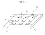
- FIG. 11 is a perspective view showing the LED backlight device according to the third embodiment of the present invention.
- the third embodiment is different from the second embodiment in the wiring structure for connecting the anode driver IC 31 and the cathode driver IC 32 to the anode electrode 14 and the cathode electrode 15 of the respective LEDs 11. Further, the constant current elements 23 ( FIG. 7 ) are not provided in the third embodiment.
- the anode driver IC 31 is connected to an end of the anode wiring 12 connected to the anode electrode 14 of the LED 11 (i.e., the endmost LED 11) closest to the anode driver IC 31 of each column of the LEDs 11.
- the cathode driver IC 32 is connected to an end of the cathode wiring 13 connected to the cathode electrode 15 of the LED 11 (i.e., the endmost LED 11) farthest from the anode driver IC 31 of each column of the LEDs 11.
- the anode electrodes 14 and the cathode electrodes 15 of the adjacent LEDs 11 are connected to each other by interconnection wirings 21.
- the LEDs 11 of each column are connected in series via the interconnection wirings 21.
- the anode electrode 14 and the cathode electrode 15 of the endmost LEDs 11 of each column are respectively connected to the anode driver IC 31 and the cathode driver IC 32 via the anode wiring 12 and the cathode wiring 13.
- the anode driver IC 31 has a function to apply current to the LEDs 11 according to the lighting signal.
- a shift register circuit, a latch circuit, a constant current circuit, an amplifier circuit and the like are integrated in the anode driver IC 31.
- the cathode driver IC 32 has a switching circuit of a large capacity capable of allowing the current from all of the LEDs 11 to flow into the switching circuit.
- anode driver IC 31 and the cathode driver IC 32 are provided on the substrate 10 in the example shown in FIG. 11 , the anode driver IC 31 and the cathode driver IC 32 are not necessarily provided on the substrate 10, but can be provided on other print circuit board (not shown) or the like.
- LED backlight device of the third embodiment is the same as those of the second embodiment, and therefore description thereof are omitted.
- the amplifier circuit of the anode driver IC 31 applies constant current to the anode electrode 14 of the LED 11 closest to the anode driver IC 31 of each column of the LEDs 11 via the anode wiring 12.
- the cathode driver IC 32 operates to allow the current to flow into the cathode driver IC 32 from the cathode electrode 15 of the LED 11 farthest from the anode driver IC 31 of each column of the LEDs 11 via the cathode wiring 13 connected to the cathode driver IC 32 by the switching circuit of a large capacity. Therefore, current flows through the LEDs 11 connected by the interconnection wirings 21 in series in each column, so that the respective LEDs 11 emit the light.
- the phosphor 30 (facing the LEDs 11) is excited by the near-ultraviolet rays or ultraviolet rays, and the phosphor 30 emits white light.
- a plurality of LEDs 11 are formed on the substrate 10 having an optical transparency, and therefore it becomes possible to accomplish a thinner LED backlight device 100 having a large surface area. Further, since the LEDs 11 of each column are connected in series, the current (the amount of which is the same as the case where the constant current elements are provided) can be applied to the respective LEDs 11 without using constant current elements. Therefore, the configuration of the LED backlight device 100 can be simplified, and the cost can be reduced.
- the description is made to the case where the LEDs 11 of each column are connected in series. However, it is also possible to connect the LEDs 11 of each row in series, or to connect the obliquely arranged LEDs 11.
- FIG. 12 is a side sectional view showing the LED backlight device according to the fourth embodiment of the present invention.
- the backlight device 100 includes a reflection film 24.
- the reflection film 24 reflects near-ultraviolet rays or ultraviolet rays emitted by the LED 11.
- a protection film 25 is formed to entirely cover the LED 11 on the first surface of the substrate 10, and the reflection film 24 is formed to cover the protection film 25.
- the reflection film 24 reflects near-ultraviolet rays and ultraviolet rays emitted in the direction opposite to the substrate 10 from the LED 11, and also reflects near-ultraviolet rays and ultraviolet rays having been reflected by the phosphor 30 or having been reflected at a boundary surface between the phosphor 30 and the substrate 10 as shown by arrows C in FIG. 12 .
- the LED 11 is peeled off from the base material 16 as was described in the first embodiment, and is pressed against the first surface of the substrate 10, so that the LED 11 is fixed to the first surface of the substrate 10 by means of intermolecular force such as hydrogen bonding. With this, the LED 11 is integrated with the substrate 10.
- the surface layer 10a can be formed on the substrate 10 as was described in the first embodiment.
- connecting portions of the anode electrode 14 and the cathode electrode 15 are formed on the LED 11 (having been integrated with the substrate 10) using, for example, a photolithographic etching method by means of an etching solution containing phosphoric acid and hydrogen peroxide and water (H 3 PO 4 :H 2 O 2 :H 2 O). Further, the anode electrode 14 and the cathode electrode 15, and the anode wiring 12 (connected to the anode electrode 14) and the cathode wiring 13 (connected to the cathode electrode 15) are formed using a deposition, a photolithographic etching method or a lift-off method.
- anode driver IC 31 and the cathode driver IC 32 are mounted to the substrate 10, and the anode wiring 12 and the cathode wiring 13 are respectively connected to the anode driver IC 31 and the cathode driver IC 32.
- the protection film 25 is formed to entirely cover the LED 11.
- the protection film 25 is composed of an organic insulation film such as a polyimide film or the like or an inorganic insulation film such as a silicon oxide film or the like.
- the reflection film 24 is formed to entire cover the protection film 25.
- the reflection film 24 is formed by forming a metal film composed of gold, aluminum, or a layered metal film composed of gold or aluminum layered with nickel, titan or the like on the surface of the substrate 10 to cover the protection film 25, and patterning the metal film.
- LED backlight device 100 Other components of the LED backlight device 100 are the same as those of the first embodiment, and therefore description thereof are omitted.
- an amplifier circuit of the anode driver IC 31 applies a constant current to the anode electrode 14 of the LED 11 via the anode wiring 12.
- the cathode driver IC 32 allows the current to flow therein from the cathode electrode 15 of the LED 11 via the cathode wiring 13, so that the LED 11 emits the light.
- the phosphor 30 (facing the LED 11) is excited by the near-ultraviolet rays or ultraviolet rays, and the phosphor 30 emits white light as shown by the arrows B in FIG. 12 .
- the near-ultraviolet rays or ultraviolet rays emitted by the LED 11 in the direction opposite to the substrate 10 and the near-ultraviolet rays or ultraviolet rays reflected by the phosphor 30 or reflected at the boundary surface between the phosphor 30 and the substrate 10 are further reflected by the reflection film 24, and are incident on the phosphor 30. Therefore, the phosphor 30 is also exited by the near-ultraviolet rays or ultraviolet rays (reflected by the reflection film 24) to emit white light.
- the reflection film 24 is provided on the LED 11 formed on the first surface of the substrate 10, and therefore it is possible to provide a thinner LED backlight device 100 providing a high intensity.
- the description is made to the LED backlight device having the single LED 11.
- the fourth embodiment i.e., the reflection film 24 and the protection film 25
- the fourth embodiment is applicable to the LED backlight device having a plurality of LEDs 11 as was described in the second and third embodiments. In this case, it becomes possible to provide the thinner LED backlight device 100 providing a high intensity and having a large surface area.
Landscapes
- Physics & Mathematics (AREA)
- Nonlinear Science (AREA)
- Mathematical Physics (AREA)
- Chemical & Material Sciences (AREA)
- Crystallography & Structural Chemistry (AREA)
- General Physics & Mathematics (AREA)
- Optics & Photonics (AREA)
- Led Device Packages (AREA)
- Led Devices (AREA)
- Liquid Crystal (AREA)
- Planar Illumination Modules (AREA)
Applications Claiming Priority (1)
| Application Number | Priority Date | Filing Date | Title |
|---|---|---|---|
| JP2007051710A JP4536077B2 (ja) | 2007-03-01 | 2007-03-01 | Ledバックライト装置及び液晶表示装置 |
Publications (2)
| Publication Number | Publication Date |
|---|---|
| EP1965251A1 true EP1965251A1 (fr) | 2008-09-03 |
| EP1965251B1 EP1965251B1 (fr) | 2011-11-02 |
Family
ID=39357668
Family Applications (1)
| Application Number | Title | Priority Date | Filing Date |
|---|---|---|---|
| EP08101946A Ceased EP1965251B1 (fr) | 2007-03-01 | 2008-02-25 | Dispositif de rétro-éclairage par DEL et dispositif LCD |
Country Status (4)
| Country | Link |
|---|---|
| US (1) | US7884374B2 (fr) |
| EP (1) | EP1965251B1 (fr) |
| JP (1) | JP4536077B2 (fr) |
| CN (1) | CN101256309B (fr) |
Families Citing this family (13)
| Publication number | Priority date | Publication date | Assignee | Title |
|---|---|---|---|---|
| JP2008218691A (ja) * | 2007-03-05 | 2008-09-18 | Oki Data Corp | Ledバックライト装置及び液晶表示装置 |
| US8013952B2 (en) * | 2007-12-25 | 2011-09-06 | Oki Data Corporation | LED backlight device and LCD device |
| JP4465385B2 (ja) * | 2007-12-25 | 2010-05-19 | 株式会社沖データ | Ledバックライト装置及び液晶表示装置 |
| JP2010147445A (ja) * | 2008-12-22 | 2010-07-01 | Panasonic Electric Works Co Ltd | 発光装置 |
| USD658601S1 (en) * | 2010-06-15 | 2012-05-01 | Toshiba Lighting & Technology Corporation | Light emitting diode module |
| USD658602S1 (en) * | 2010-06-15 | 2012-05-01 | Toshiba Lighting & Technology Corporation | Light emitting diode module |
| KR101679077B1 (ko) | 2010-07-02 | 2016-11-24 | 엘지디스플레이 주식회사 | 백라이트 유닛 및 이를 구비한 액정표시장치 |
| CN102339935B (zh) * | 2010-07-15 | 2015-07-08 | 展晶科技(深圳)有限公司 | 覆晶式led封装结构 |
| KR20120019140A (ko) * | 2010-08-25 | 2012-03-06 | 삼성전자주식회사 | 액정표시장치 |
| KR101953822B1 (ko) | 2012-08-14 | 2019-03-06 | 삼성디스플레이 주식회사 | 액정 표시 장치 |
| US10520769B2 (en) * | 2014-10-31 | 2019-12-31 | eLux, Inc. | Emissive display with printed light modification structures |
| CN105552087B (zh) * | 2015-12-30 | 2018-04-13 | 广东省半导体产业技术研究院 | 一种led微型阵列透明显示装置 |
| CN107639934A (zh) * | 2017-09-30 | 2018-01-30 | 北京印刷学院 | 程控多波长可变频段uvled固化光源 |
Citations (5)
| Publication number | Priority date | Publication date | Assignee | Title |
|---|---|---|---|---|
| US5813753A (en) * | 1997-05-27 | 1998-09-29 | Philips Electronics North America Corporation | UV/blue led-phosphor device with efficient conversion of UV/blues light to visible light |
| JPH11232920A (ja) | 1998-02-13 | 1999-08-27 | Omron Corp | 面光源装置及び同装置用の光取り込み口モジュール |
| EP1385215A2 (fr) * | 2002-07-08 | 2004-01-28 | Nichia Corporation | Dispositif semiconducteur à nitrure avec un substrat soudé et procédé de fabrication correspondant |
| EP1521235A2 (fr) * | 2003-10-03 | 2005-04-06 | LumiLeds Lighting U.S., LLC | Rétroéclairage pour un affichage à cristaux liquides comprenant un réseau bidimensionnel de diodes électroluminescentes |
| US20060158581A1 (en) * | 1997-05-16 | 2006-07-20 | Kabushiki Kaisha Toshiba | Image display device and light emission device |
Family Cites Families (22)
| Publication number | Priority date | Publication date | Assignee | Title |
|---|---|---|---|---|
| JP3466365B2 (ja) | 1996-02-27 | 2003-11-10 | 京セラ株式会社 | 半導体基板の製造方法 |
| WO1997048138A2 (fr) | 1996-06-11 | 1997-12-18 | Philips Electronics N.V. | Dispositifs emettant de la lumiere visible, y compris des diodes emettant de la lumiere ultraviolette et des elements fluorescents excitables par les ultraviolets et emettant de la lumiere visible et procede de production de tels dispositifs |
| JPH1123290A (ja) | 1997-06-27 | 1999-01-29 | Japan Aviation Electron Ind Ltd | 多重化光干渉角速度計 |
| JP2000133006A (ja) | 1998-10-29 | 2000-05-12 | Sanyo Electric Co Ltd | 面光源 |
| DE60045514D1 (de) * | 1999-09-01 | 2011-02-24 | Osram Opto Semiconductors Gmbh | Organische elektrolumineszente vorrichtung und verfahren zu derer herstellung |
| DE10137042A1 (de) * | 2001-07-31 | 2003-02-20 | Patent Treuhand Ges Fuer Elektrische Gluehlampen Mbh | Planare Lichtquelle auf LED-Basis |
| JP2003068109A (ja) * | 2001-08-23 | 2003-03-07 | Sony Corp | 照明装置及び投影装置 |
| JP2004055772A (ja) * | 2002-07-18 | 2004-02-19 | Citizen Electronics Co Ltd | Led発光装置 |
| CN100353234C (zh) * | 2002-08-30 | 2007-12-05 | 三菱化学株式会社 | 彩色液晶显示装置 |
| JP2004119634A (ja) | 2002-09-25 | 2004-04-15 | Toshiba Lighting & Technology Corp | 発光装置 |
| CN100573932C (zh) * | 2003-05-16 | 2009-12-23 | 晶元光电股份有限公司 | 具有粘结层的发光二极管及其制造方法 |
| JP4488702B2 (ja) | 2003-07-30 | 2010-06-23 | 株式会社沖データ | 半導体装置の製造方法 |
| JP2005079369A (ja) * | 2003-09-01 | 2005-03-24 | Oki Data Corp | 半導体複合装置の製造方法 |
| JP2005093649A (ja) * | 2003-09-17 | 2005-04-07 | Oki Data Corp | 半導体複合装置、ledプリントヘッド、及び、それを用いた画像形成装置 |
| JP4672329B2 (ja) * | 2003-10-22 | 2011-04-20 | 株式会社沖データ | 半導体装置、及び、それを用いたledプリントヘッド、画像形成装置、半導体装置の製造方法 |
| US7195944B2 (en) | 2005-01-11 | 2007-03-27 | Semileds Corporation | Systems and methods for producing white-light emitting diodes |
| JP4770199B2 (ja) * | 2005-03-01 | 2011-09-14 | パナソニック電工株式会社 | 照明光源、照明装置、及び表示装置 |
| JP4663357B2 (ja) | 2005-03-15 | 2011-04-06 | 株式会社沖データ | 半導体装置 |
| JP5076282B2 (ja) | 2005-04-28 | 2012-11-21 | 三菱化学株式会社 | 表示装置 |
| KR100708717B1 (ko) * | 2005-10-11 | 2007-04-17 | 삼성에스디아이 주식회사 | 전자 방출 발광 소자 및 이를 이용한 평판 디스플레이 장치 |
| US7481563B2 (en) * | 2006-09-21 | 2009-01-27 | 3M Innovative Properties Company | LED backlight |
| JP2008218691A (ja) * | 2007-03-05 | 2008-09-18 | Oki Data Corp | Ledバックライト装置及び液晶表示装置 |
-
2007
- 2007-03-01 JP JP2007051710A patent/JP4536077B2/ja not_active Expired - Fee Related
-
2008
- 2008-02-25 EP EP08101946A patent/EP1965251B1/fr not_active Ceased
- 2008-02-28 US US12/038,827 patent/US7884374B2/en not_active Expired - Fee Related
- 2008-02-29 CN CN2008100823304A patent/CN101256309B/zh not_active Expired - Fee Related
Patent Citations (5)
| Publication number | Priority date | Publication date | Assignee | Title |
|---|---|---|---|---|
| US20060158581A1 (en) * | 1997-05-16 | 2006-07-20 | Kabushiki Kaisha Toshiba | Image display device and light emission device |
| US5813753A (en) * | 1997-05-27 | 1998-09-29 | Philips Electronics North America Corporation | UV/blue led-phosphor device with efficient conversion of UV/blues light to visible light |
| JPH11232920A (ja) | 1998-02-13 | 1999-08-27 | Omron Corp | 面光源装置及び同装置用の光取り込み口モジュール |
| EP1385215A2 (fr) * | 2002-07-08 | 2004-01-28 | Nichia Corporation | Dispositif semiconducteur à nitrure avec un substrat soudé et procédé de fabrication correspondant |
| EP1521235A2 (fr) * | 2003-10-03 | 2005-04-06 | LumiLeds Lighting U.S., LLC | Rétroéclairage pour un affichage à cristaux liquides comprenant un réseau bidimensionnel de diodes électroluminescentes |
Non-Patent Citations (2)
| Title |
|---|
| LIU P C ET AL: "Wafer bonding for high-brightness light-emitting diodes via indium tin oxide intermediate layers", THIN SOLID FILMS, ELSEVIER-SEQUOIA S.A. LAUSANNE, CH, vol. 478, no. 1-2, 1 May 2005 (2005-05-01), pages 280 - 285, XP004774134, ISSN: 0040-6090 * |
| MURAI AKIHIKO ET AL: "Hexagonal pyramid shaped light-emitting diodes based on ZnO and GaN direct wafer bonding", APPLIED PHYSICS LETTERS, AIP, AMERICAN INSTITUTE OF PHYSICS, MELVILLE, NY, vol. 89, no. 17, 26 October 2006 (2006-10-26), pages 171116 - 171116, XP012086524, ISSN: 0003-6951 * |
Also Published As
| Publication number | Publication date |
|---|---|
| US20080211993A1 (en) | 2008-09-04 |
| EP1965251B1 (fr) | 2011-11-02 |
| US7884374B2 (en) | 2011-02-08 |
| JP4536077B2 (ja) | 2010-09-01 |
| CN101256309B (zh) | 2013-07-17 |
| CN101256309A (zh) | 2008-09-03 |
| JP2008218099A (ja) | 2008-09-18 |
Similar Documents
| Publication | Publication Date | Title |
|---|---|---|
| US7884374B2 (en) | LED backlight device and LCD device | |
| US7863614B2 (en) | LED backlight device and LCD device | |
| US7884371B2 (en) | LED backlight device and LCD device | |
| US8023070B2 (en) | LED backlight device and LCD device | |
| US12310161B2 (en) | Light-emitting diode unit for display comprising plurality of pixels and display device having same | |
| JP7282138B2 (ja) | 表示装置 | |
| US9997561B2 (en) | Light emitting diode module, display panel having the same and method of manufacturing the same | |
| US9666600B2 (en) | Direct bandgap substrates and methods of making and using | |
| KR102039838B1 (ko) | 마이크로 led 디스플레이 화소 조립체 및 이의 제조방법 | |
| JP5207812B2 (ja) | 発光デバイスおよび発光デバイスの製造方法 | |
| JP4640427B2 (ja) | GaN系半導体発光素子、発光素子組立体、発光装置、GaN系半導体発光素子の製造方法、GaN系半導体発光素子の駆動方法、及び、画像表示装置 | |
| US8013952B2 (en) | LED backlight device and LCD device | |
| KR20190137458A (ko) | Led를 이용한 디스플레이 모듈 제조방법 | |
| US8104907B2 (en) | Remote wavelength converting material configuration for lighting | |
| US7471040B2 (en) | Mixed-color light emitting diode apparatus, and method for making same | |
| KR20220027177A (ko) | 디스플레이 패널 및 그의 제조 방법 | |
| KR20200079434A (ko) | 발광 장치 및 표시 장치 | |
| KR20260031923A (ko) | Led 표시장치 및 이의 제조방법 |
Legal Events
| Date | Code | Title | Description |
|---|---|---|---|
| PUAI | Public reference made under article 153(3) epc to a published international application that has entered the european phase |
Free format text: ORIGINAL CODE: 0009012 |
|
| AK | Designated contracting states |
Kind code of ref document: A1 Designated state(s): AT BE BG CH CY CZ DE DK EE ES FI FR GB GR HR HU IE IS IT LI LT LU LV MC MT NL NO PL PT RO SE SI SK TR |
|
| AX | Request for extension of the european patent |
Extension state: AL BA MK RS |
|
| 17P | Request for examination filed |
Effective date: 20090303 |
|
| AKX | Designation fees paid |
Designated state(s): DE FR GB NL |
|
| 17Q | First examination report despatched |
Effective date: 20090511 |
|
| GRAP | Despatch of communication of intention to grant a patent |
Free format text: ORIGINAL CODE: EPIDOSNIGR1 |
|
| GRAS | Grant fee paid |
Free format text: ORIGINAL CODE: EPIDOSNIGR3 |
|
| GRAA | (expected) grant |
Free format text: ORIGINAL CODE: 0009210 |
|
| AK | Designated contracting states |
Kind code of ref document: B1 Designated state(s): DE FR GB NL |
|
| REG | Reference to a national code |
Ref country code: GB Ref legal event code: FG4D |
|
| REG | Reference to a national code |
Ref country code: DE Ref legal event code: R096 Ref document number: 602008011007 Country of ref document: DE Effective date: 20111229 |
|
| REG | Reference to a national code |
Ref country code: NL Ref legal event code: T3 |
|
| PLBE | No opposition filed within time limit |
Free format text: ORIGINAL CODE: 0009261 |
|
| STAA | Information on the status of an ep patent application or granted ep patent |
Free format text: STATUS: NO OPPOSITION FILED WITHIN TIME LIMIT |
|
| 26N | No opposition filed |
Effective date: 20120803 |
|
| REG | Reference to a national code |
Ref country code: DE Ref legal event code: R097 Ref document number: 602008011007 Country of ref document: DE Effective date: 20120803 |
|
| REG | Reference to a national code |
Ref country code: FR Ref legal event code: PLFP Year of fee payment: 9 |
|
| REG | Reference to a national code |
Ref country code: FR Ref legal event code: PLFP Year of fee payment: 10 |
|
| REG | Reference to a national code |
Ref country code: FR Ref legal event code: PLFP Year of fee payment: 11 |
|
| PGFP | Annual fee paid to national office [announced via postgrant information from national office to epo] |
Ref country code: FR Payment date: 20210113 Year of fee payment: 14 Ref country code: NL Payment date: 20210113 Year of fee payment: 14 |
|
| PGFP | Annual fee paid to national office [announced via postgrant information from national office to epo] |
Ref country code: GB Payment date: 20210217 Year of fee payment: 14 Ref country code: DE Payment date: 20210209 Year of fee payment: 14 |
|
| REG | Reference to a national code |
Ref country code: DE Ref legal event code: R119 Ref document number: 602008011007 Country of ref document: DE |
|
| REG | Reference to a national code |
Ref country code: NL Ref legal event code: MM Effective date: 20220301 |
|
| GBPC | Gb: european patent ceased through non-payment of renewal fee |
Effective date: 20220225 |
|
| PG25 | Lapsed in a contracting state [announced via postgrant information from national office to epo] |
Ref country code: NL Free format text: LAPSE BECAUSE OF NON-PAYMENT OF DUE FEES Effective date: 20220301 Ref country code: FR Free format text: LAPSE BECAUSE OF NON-PAYMENT OF DUE FEES Effective date: 20220228 |
|
| PG25 | Lapsed in a contracting state [announced via postgrant information from national office to epo] |
Ref country code: GB Free format text: LAPSE BECAUSE OF NON-PAYMENT OF DUE FEES Effective date: 20220225 Ref country code: DE Free format text: LAPSE BECAUSE OF NON-PAYMENT OF DUE FEES Effective date: 20220901 |